
11 | Projects
There are a vast number and a wide range of useful and interesting audio circuits to be found in books and magazines, and on the internet varying in functionality and complexity from the almost trivial to the most elaborate imaginable. Typical audio projects might be broken down into three general types which can be broadly categorised as producers, modifiers, and amplifiers of sound. Within each category circuits will be encountered to suit every taste and level of experience.
The introductory projects presented here naturally stick close to the novice end of the spectrum. They should however provide sufficient insight and understanding to allow the reader to extend their explorations to whatever level and in whatever direction they so desire. Each of the three categories mentioned above covers a wide range of applications and approaches. Some of the key circuit types and classes are listed here under each of the three headings.
Sound producers include both sound and vibration detection devices such as microphone and pickup based projects, and signal generators such as oscillators, synthesisers, and general noise making circuits.
Sound modifiers range from simple filter and EQ circuits through to the vast array of audio effects which are available, including such things as distortion, phaser, flanger, vibrato, tremolo, echo, delay, and so on. This category also includes the wide range of ancillary circuits for controlling and modulating effects, such as LFOs and envelope generators.
Sound amplifiers are fairly self explanatory but there is still quite a range. Beyond the generic audio power amplifier (including home hifi, studio monitor, and PA and sound system style amps) there are also headphone amps, guitar and instrument amps, portable, battery powered, and practice amps, along with other specialist amplifiers employed in specific roles such as mic pre-amps, loud hailers, phono pre-amps, etc.
The three circuits presented as projects in this chapter include an example from each of these three categories. This gives a flavour of the range of audio projects which can easily be undertaken by the novice electronics experimenter. Guidance is offered on prototyping, modifying, testing, and building. A short introduction such as this can only scratch the surface of what is possible, and ultimately the limits of what can be achieved are set only by the imagination and ingenuity of the electronics project builder.
Project I – Low Power Audio Amplifier
One of the most ubiquitous integrated circuits encountered in audio electronics is a single chip low power audio amplifier called the 386. It comes from two main manufacturers who designate it respectively the LM386 and the NJM386 (aka JRC386). The consensus seems to be that the latter is usually more stable and on the whole to be preferred, and this has certainly been my experience. The former is however often more easily procured, and in general, with a little care, either will usually do the job in any given circuit.
This project is quite closely related to a design from runoffgroove.com called the Ruby, one of very many 386 based amplifier circuits to be found online. The main differences between the Ruby and the design presented here (see Figure 11.1) are:
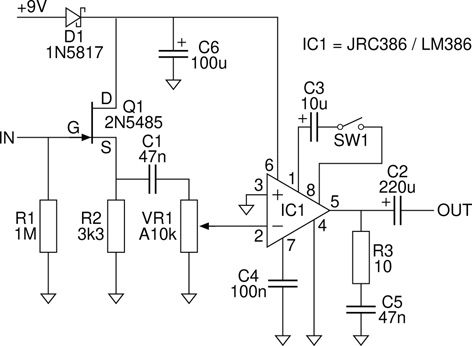
Figure 11.1 Circuit diagram for a simple 386 based low power (< 1W) audio power amplifier. Similar circuits are often described as guitar practice amps but they are ideal for use as a generic lo-fi utility audio amplifier well suited to experimentation and general audio amplification.
1. The addition of a reverse voltage protection diode. (The 386 is easily damaged by applying a reverse voltage to its power supply.)
2. The JFET used has been changed from an MPF102 to a 2N5485. (This is mainly a question of availability – see Chapter 17 for a discussion on substituting transistors.)
3. The sizes of resistors R1 and R2 have been changed to more readily available values than those specified in the original Ruby design.
4. Where the Ruby uses a gain pot connected between pins one and eight of the 386, this is replaced with an spst switch and a ten microfarad capacitor. With the switch open the circuit operates at its lowest gain setting. Closing the switch raises the internal gain of the 386 from its default value of 20 up to its maximum level of 200.
As is always the case when working with an unfamiliar component it is highly recommended to review the data sheet for the 386 in order to fully understand these configuration options. A quick internet search will immediately yield this document. These data sheets are also well worth seeking out for the various integrated circuits encountered, as they often include useful example circuits. This is certainly the case with the 386 where a number of instructive circuit suggestions can be found. Figure 11.1 shows the circuit diagram for the particular design which is presented in this section.
Main Circuit Elements
The 368 low voltage audio power amplifier at the heart of this circuit is an eight pin DIL package IC (the type of chip pictured on the right of Figure 18.1 (p. 315)), designated IC1 in the circuit diagram. Similar to an opamp (opamp circuits are discussed in Chapter 18), the 386 has two inputs designated noninverting (+) and inverting (−), and the output is the amplified difference between these two inputs. Unlike opamps, which amplify voltage but do not have the current sourcing capability to drive a loudspeaker, power amplifiers like the 386 are designed to connect directly to a low impedance load (typically 8 for a standard moving coil loudspeaker).
Also in common with typical opamp practice one of the two inputs is usually wired to ground, in this case the noninverting input on pin three. The signal to be amplified is presented at pin two and the amplified (and inverted) result emerges from the chip at pin five. Pins four and six provide the necessary connections to the power supply, in this case usually a standard 9V battery, although the chip can generally operate from a supply anywhere in the range 4V to 12V. The highest power variant, the LM386N-4, can be operated on a power supply ranging up to a maximum of 18V. Meanwhile pins one and eight allow for control over the amplifier’s gain, and finally pin seven (usually labelled ‘Bypass’) is connected through a capacitor to ground in order to enhance the stability of the amplifiers operation, especially at high gain.
As mentioned above, the 386 comes in a few variants delivering different maximum output power levels ranging from 250mW up to about 1W. The upper end of this range is rather optimistic and if reasonably low levels of signal distortion are desired the maximum achievable output levels will be commensurately lower. On the other hand in its common application as an electric guitar practice amp, driving the chip to higher levels of distortion can result in quite a satisfyingly dirty sound. Surprisingly high sound levels can be coaxed out of this diminutive little chip, and it is quite capable of driving even moderately large loudspeaker drivers (or multi speaker cabinets) as well as making for an excellent compact utility amplifier when used in combination with a two and a half inch, half watt speaker.
The input buffer is comprised of a JFET (Q1) and two associated resistors (R1 and R2). It significantly improves the sound of this amp as compared to that of more rudimentary unbuffered 386 designs, especially when used connected directly to an electric guitar with passive pickup circuitry. This improvement is achieved primarily due to the increased input impedance which this input circuitry provides. Connecting directly to the input pins of the 386 presents an input impedance of about 50kΩ whereas here the input impedance is 1MΩ, set by the value of the resistor R1 connected from the JFET’s gate to ground. The JFET itself presents an extremely high input impedance typically in the GΩ range (Evans, 1972, p. 73) and often considered to be infinite for all practical purposes (Sedra and Smith, 1987, p. 295). As such it does not have much effect on the overall input impedance as it appears in parallel with the 1M resistor to ground.
A high input impedance is of particular value here because a guitar pickup has an output impedance which is also very high, typically in the hundreds of kilohms range. For optimum interfacing the input impedance typically wants to be about an order of magnitude larger than the output impedance which it is connected to. This provides for efficient transfer of signal from output to input and best preserves the tone of the guitar or other sound source. As such this JFET based input buffer also operates very well when interfacing to a piezo pickup. As mentioned in Chapter 20, piezos have an extremely high output impedance and as such benefit from connection to as high an input impedance as possible.
The observations in this section should serve to illustrate and re-enforce the idea that a solid grasp of impedance and the role it plays in interfacing audio circuitry is vitally important to developing a good understanding of the ins and out of signal flow and audio circuit design and analysis.
Working with discrete transistors it is always necessary to pay attention to the pinout of the particular device used. Pinouts are not consistent across transistors, even of the same type. Reference to the device’s data sheet should be made in order to confirm the arrangement of the three terminals. In the case of the 2N5485 used here the pinout is shown in Figure 11.2. Transistor data sheets will include this information, usually in the form of a diagram similar to the one included here.
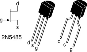
Figure 11.2 The pinout for the input buffer 2N5485 JFET.
Input and output coupling capacitors are common elements found in many audio circuits. They will often be referred to as DC blocking capacitors as one of their main jobs is to make sure that signals moving from one section of a system to the next have the correct DC bias applied to them. A guitar pickup generates an AC signal which varies up and down either side of ground or zero volts, but an oscillator circuit for instance is quite likely to present a signal whose midpoint lies at a positive voltage most probably halfway between ground and the positive power rail voltage powering the circuit. A general purpose amplifier must be able to cope with both of these signals, contending with these two very different signal bias conditions seamlessly.
The inputs on the 386 are internally biased and are designed to take ground referenced input signals, so while the guitar signal might couple directly into the chip without problem, attempting to do the same with the oscillator signal would result in massive distortion at best and a blown amp at worst. The solution is however very straightforward, an input coupling capacitor is placed between the incoming signal and the internally biased 386 input pin. Recalling that capacitors block low frequencies and pass high frequencies it should come as no surprise that any DC offset between signal and input will be soaked up in charging the capacitor while the AC component of the signal continues on into the input pin. In the circuit in Figure 11.1 this job is accomplished by the 47nF capacitor labelled C1 which feeds into the volume pot VR1.
Similarly at the output of the 386 the signal produced will include an offset bias equal to half the supply voltage. Thus if the amp is powered from a 9V battery then the signal will vary either side of 4.5V. However the loudspeaker which is likely to be connected to the amp’s output wants to see a signal with zero bias voltage, otherwise the speaker driver’s voice coil is likely to be burned out before long. Again a simple capacitor between output and speaker resolves the difficulty, in this case the 220µF capacitor C2 between pin 5 and OUT.
The input and output coupling capacitors will also tend to affect the tone of the amplifier. Each will combine with their respective following resistances to ground, to form high pass filters (see Chapter 13). Using Eq. 13.13, the cutoff frequencies can be estimated. The large 220µF capacitor on the output, in combination with the 8 loudspeaker, will pass all but the lowest audio frequencies unaltered.
The smaller input capacitor C1 (in combination with the 10kΩ volume pot VR1, and ignoring the effect of the larger input impedance of the 386) will have a more significant effect, rolling off the level within a significant range of the lower band of audio frequencies delivered to the input of the 386.
These calculations are somewhat simplistic in this context, but give a good sense of the general behaviour to be expected. Different sized capacitors can thus be used in this way to alter the overall tone of the amplifier to suit personal taste or specific applications. It makes sense to roll off any undesired low frequencies before amplification, especially since the 386, being a very modest amplifier, is easily overwhelmed especially by low frequencies.
The volume pot VR1 feeding pin two of the 386 operates as a voltage divider exactly as described in Chapter 12 in the section on Attenuators and Volume Controls. When the pot is turned fully down pin 2 of the 386 is connected directly to ground and as such sees no input signal at all. As the pot is turned up the level of signal reaching pin 2 steadily increases until finally the full signal voltage from the input buffer section is presented at pin 2 for amplification. Using a pot with an audio or log taper in this position is likely to give the best volume control characteristic. Using a linear taper pot will work fine but the volume control will bunch most of the level change into the first half of the pot’s rotation, with the latter half having little further effect on the output volume. As discussed in Chapter 12, using a log pot will mitigate this problem and provide a more user friendly behaviour for the amplifier’s volume control. The A in A10k specifying the value for VR1 indicates that an audio taper is preferred.
The gain switch and capacitor (SW1 and C3) which can be found bridging pins one and eight of the 386 provide a simple lo/hi gain option. Reference should be made to the data sheet for the 386 IC in order to see the effect of these components. With an open circuit between pins 1 and 8 the 386 amplifier has a native voltage gain of 20. That is to say, whatever input signal is presented at pin 2 the amplifier will endeavour to output a signal identical in shape but twenty times as large. Of course this being a rather simple amplifier some distortion is to be expected and as always the output is also limited by the power supply used, so with a single nine volt battery the output signal can certainly not extend beyond the range zero volts to nine volts.
Once the gain switch is closed the gain jumps up to 200. As is detailed in the data sheet intermediate gains can be achieved by placing a resistor between pins 1 and 8, and so a smoothly varying gain can be achieved using a pot. Given that the input volume pot already provides continuous control over the signal level, and in the interests of both simplicity and variation, a switch has been employed in this design. The capacitor is as recommended in the data sheet and is intended to assist in maintaining stability at high gains.
The stabilisation capacitor C4 connected to pin 7 also helps prevent stability and oscillation problems, again especially when in high gain mode. The addition of a capacitor on pin 7 is once more simply a case of following the advice given in the chip’s data sheet. A common issue which can be encountered when amplifiers with high gain are employed is what are called parasitic oscillations where some frequencies can result in runaway amplification causing the amplifier to squeal or screech even when there is no input signal present. Often a judiciously deployed capacitor is the best solution to eradicating such unwanted oscillations, and in this case the connection on pin 7 is, according to the data sheet, the place to connect just such a capacitor.
The zobel network composed of R3 and C5 connected to the output in this circuit is a standard method of interfacing to a loudspeaker. A typical moving coil loudspeaker is an inductive load as the presence of the word ‘coil’ in its name might suggest. Recall that an inductor is just a coil of wire and so it should come as no surprise that a component which includes a coil as the primary electrical element used in its construction exhibits significant inductance. Remember that for an inductor impedance increases with frequency (inductors pass low frequencies and block high frequencies). An amplifier prefers to see a steady load across all frequencies in order to operate at its best. For a typical 8 loudspeaker (remember most speakers are rated 4, 8, or 16Ω, with 8Ω being by far the most common) the series resistor-capacitor network shown will do a pretty good job of flattening the overall load impedance which the amplifier sees, allowing it to perform to its best.
With rising frequency the coil impedance rises as the capacitor’s impedance falls. Combined with the resistive impedances of both R3 and the wire in the coil of the loudspeaker, the overall impedance loading the amplifier is much more stable across frequencies than would be the case were the loudspeaker connected without any compensating network in parallel. This can have a very substantial effect on the operation of the circuit as can be seen from the oscilloscope traces in Figure 11.3. In each case the top trace is the input signal while below it is shown the amplifier’s output. In situation (a) the zobel network is present exactly as shown in the circuit diagram. The only change made in order to obtain the traces in (b) is that the zobel network has been removed from the circuit. A large amount of high frequency instability has been introduced.

Figure 11.3 Zobel network helps maintain amplifier stability.
Both plots were obtained with the amplifier running at low gain. Notice that the legend states that channel 1 was set to 50mV per division and channel 2 was set to 1V per division. From this it is a simple matter to confirm that a gain of approximately twenty was indeed applied.
It is also easy enough to estimate the frequency of the test signal used given the 250µSec per division label also present. A 1kHz test tone is a very commonly used audio test signal, and so it should come as no surprise to arrive at this result here also. This is a very common but very simple approach to loudspeaker compensation. More advanced approaches (e.g. Leach, 2004) can achieve superior results in high quality audio systems but would certainly be overkill in a project such as this.
The reverse voltage protection diode D1 connected from the +9V supply line into the circuit illustrates one common method of implementing reverse polarity protection. In general it is important not to reverse the power connections to a circuit. If a standard nine volt battery is being used to power a circuit, it is very easy to accidentally touch the terminals to the battery clip the wrong way round when changing the battery. Without the protection diode to block the reverse voltage, if the terminals were to touch the wrong contacts on the battery clip even for a moment the 386 would likely be destroyed.
The reservoir/smoothing capacitor C6 connected between the +9V and 0V rails is another common circuit element encountered in many circuits. Even when not shown explicitly on a circuit diagram it can be a good addition depending on the characteristics and function both of the circuit and the power supply being used to run it. A large capacitor across the power supply can serve two useful functions.
Firstly it can act as a charge reservoir. When a high level transient arrives at the amplifier the circuit will require a short burst of high current in order to effectively amplify this signal peak. Any power supply will have a limit as to how much current it can provide and this can easily be exceeded for a brief moment by the requirements of amplifying such a transient. The capacitor can not hold very much charge but what it can hold it can release very quickly indeed and so for a short time it can augment the current coming directly from the power supply. Once the transient has passed the capacitor will replenish its charge ready for the arrival of the next big transient for which the power supply will need its assistance in supplying sufficient current to amplify cleanly.
The second job which the power supply capacitor can perform is in helping to eliminate any noise or ripple present on the supply. Since a circuit effectively uses the power supply as a voltage reference any noise present on the supply can get transferred onto the audio signal passing through the circuit. A well regulated supply is crucial to clean audio, and the capacitor can play a large role in making sure this is achieved. Low frequency ripple often appears in a voltage derived from the mains. Mains power is a large AC signal with a frequency of 50Hz or 60Hz, and when this gets into the audio signal it results in an annoying and all too familiar hum. Higher frequency noise can originate from many other places but one way or another it is highly desirable to keep it from getting into the audio.
The exact size of the smoothing capacitor is not crucial. Typically 100µF or larger is common. It needs to be big so that it can hold enough charge to make for an effective reservoir. The only problem with large capacitors is that they are usually a little less effective at working with high frequencies and so if high frequency interference is a potential issue then a second much smaller capacitor is often placed in parallel with the reservoir cap in order to deal with smaller but higher frequency noise on the power line. Sometimes theses smaller decoupling capacitors can be found placed throughout a circuit. Most commonly one can be found right next to the power pin of every IC on many commercially produced circuit boards. Often this is overkill but if a noise problem is encountered which cannot be eliminated at source, it may turn out to be a simple solution.
Breadboard Layout, Circuit Testing, and Modification
When a new circuit is being investigated, a breadboard build is almost always the best first step in the process. Because components can be easily plugged into and out of a breadboard they allow for simple testing and experimentation prior to soldering up a permanent version of the circuit on stripboard or PCB. Preparing a good, well laid out design prior to starting work on the board itself is to be highly recommended. The situation can quickly become messy and confusing when attempting to build directly from the circuit diagram. Much better to take some time to design a good layout first. This can be done easily by drawing on squared paper, but it is probably much simpler to use a software package designed for the purpose. There are many options available but for a good free solution a program called DIYLC (‘Do-It-Yourself Layout Creator’) serves very well. The layouts reproduced in this book were specifically generated in order to obtain optimum printing clarity and resolution but a similar on screen result is possible using DIYLC.
Figure 11.4 386 amp breadboard layout.
Figure 11.4 shows a possible breadboard layout for the 386 amplifier circuit. The two rows of jumper wires across the top of the board are a common way of distributing 0V and +9V up and down both sides of the board. This is often convenient as both power and ground connections are often required at various points around the circuit built on the middle section of the breadboard. These outer buses do not have to be used for power connections but they most often are. Very occasionally on more complex circuit layouts it can be convenient to use one of these buses to make a connection which would otherwise prove messy. Maintaining a clean layout is a great benefit when it comes to debugging a circuit, so it is well worth spending the time at the outset to get everything positioned, connected, and labelled in a clear and consistent fashion.
Symbols are often provided by layout software to indicate off-board components such as jacks, switches, pots, and power connectors. The style adopted in this book has been to exclusively use text labels for all off-board components (in this circuit these include power, in/out jacks, gain switch, and volume pot). This makes everything a little easier to lay out and avoids big looping connection wires snaking around the figure. Such graphical conventions are simply a matter of individual taste. I/O jacks are labelled with a (+) for the signal connection, usually the tip of a TS phone jack, and a (−) for the ground connection, usually the sleeve of a TS phone jack. Other components have their terminals named and numbered in a logical fashion.
The OUT connections may either go to a jack for connection to a speaker cab, or they may be connected directly to the terminals of an appropriate loudspeaker if this is desired. Both options can even be provided by using a switching jack. The switch SW1 is a simple spst device, and as such the order of connections does not actually matter. Pots have three terminals and throughout this book these terminals are numbered 1–3, with pin 1 being the left or counterclockwise connection point, pin 2 being the middle, variable connection, and pin 3 being the right or clockwise terminal. Thus turning the pot counterclockwise (conventionally considered down) moves 2 towards 1, and turning it clockwise (conventionally considered up) moves 2 towards 3.
Often it is not immediately obvious from a circuit diagram which way round terminals 1 and 3 should be connected in order to achieve the desired effect. If the wrong orientation is initially selected no harm will ensue, the operation of the circuit will simply be counter intuitive with ‘up’ becoming ‘down’ and vice versa. Confirming and carefully noting the correct connection orientation for expected operation is one task easily performed during the breadboarding phase of circuit test and development. Once it has been confirmed, correct labelling on the diagram will avoid a mixup later on down the line.
With a layout such as that shown in Figure 11.4 the process of breadboard construction is a simple matter, and with all components to hand should take no time at all. Always carefully check and recheck all connections before connecting power to the circuit. Pay particular attention to power and ground connections, making sure that none have been accidentally inverted. It is worth bearing in mind that the 386 will not tolerate reverse power connection and this is one sure way of burning out the chip.
Once the breadboard circuit is up and running, modifications can be tried and different component values can be compared. Try smaller coupling capacitors for a more trebly sound. Experiment with different JFETs in the input buffer. See what difference a bigger volume pot makes, or compare linear and log pot tapers. Revert to a gain pot between pins 1 and 8. Run at lower or higher voltages (within the limits the 386 can handle). Listen without the zobel network. See how well it works into different loudspeaker loads. Compare operation with and without the stabalising capacitor on pin 7, with particular attention to high gain operation. After all these variations have been examined a much better feel for how the circuit works, and what it is capable of will have been gained, and so the final design to be soldered up as a permanent circuit will provide the best performance possible.
Along with all these modifications there are a myriad tests and measurements which can be performed in order to quantify and visualise the consequences of each change. One invaluable tool at this stage is the oscilloscope. An example of the kind of information which can be obtained was shown above when discussing the role of the zobel network. Figure 11.5 below offers another snapshot into the way in which this circuit works. Here the low and high gain settings are being compared. As before the top trace in each case is the input signal and the bottom trace is the output, and again the settings used to take the measurements are noted below the figures.
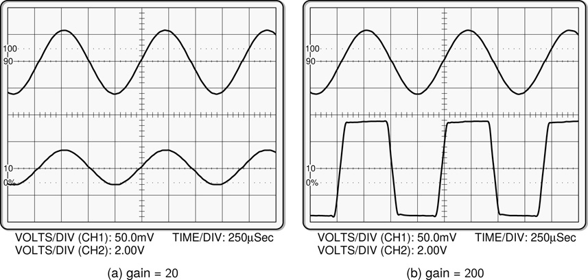
Figure 11.5 A 1kHz test tone at gains of 20 and 200.
Notice that the output has been displayed using the same settings in both instances. Clearly with the gain at 200 the output is not ten times bigger, and furthermore the clean sine wave input has been distorted badly into something more closely approximating a square wave. Close to the centreline the amplification appears to have been performed quite cleanly. However the amplifier quickly runs out of headroom as it attempts to extend the output signal beyond the range facilitated by the available power supply voltages, and so the signal is clipped at round about +1V at the bottom and +8V at the top, leading to the squared off signal seen in Figure 11.5b. This is classic signal clipping resulting from overdriving the amplifier. In listening to these two signals the second is louder certainly but not 20dB louder. It is however vastly more distorted. In this instance, this can actually work quite well as a basic electric guitar distortion effect.
Stripboard Layout and Final Project Build
With the design finalised on breadboard it is time to draft a stripboard layout ready for building. Figure 11.6 illustrates a good compact stripboard design. Notice that two copies of the board are shown. Above is the component side of the board while below it the board has been flipped over to show the copper side where all the soldering happens. The only things shown on the copper side are holes and breaks. Holes (the black rings on the diagram) just identify locations where mounting holes might be drilled through the board to allow standoffs to attach the board to whatever enclosure it is going to be built into.
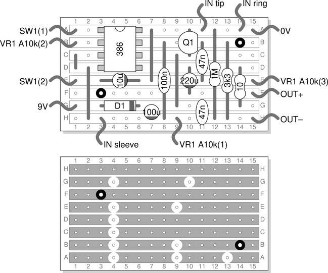
Figure 11.6 386 amp stripboard layout.
Breaks (the white rings on the diagram) are places where the horizontal copper strips of the stripboard need to be broken so that different sections of the same strip can be used to make different connections in the circuit. Notice that a DIL package IC will always need to have a column of breaks running under it to isolate the legs on either side of the chip (in this case breaks at locations 4A through 4D). Notice also that the strip indexing has been reversed on the copper side since when the board is flipped over the top row ends up at the bottom and vice versa. Great care must be taken to make sure that everything gets correctly located on the board as once soldering has happened it can be very difficult to undo any mistakes. Breaks in the wrong place are even more difficult to remedy and it is all too easy to mirror the required positions if sufficient care is not taken.
The step by step build procedures described in Chapter 10 should be followed in order to complete the project. Notice one small tweak which has been introduced in this final circuit when compared to the (otherwise identical) design provided for the breadboard layout. There will often be one or two housekeeping details which are not included until the final version. In this case automatic on/off switching has been implemented as described in Chapter 15.
Instead of a TS input jack a TRS jack has been used. The ring terminal is connected to the negative of the power supply while all other ground connections in the circuit are connected with the input jack’s sleeve in the usual fashion. This means that even after the battery or other power supply has been attached, the circuit is not powered up until a TS jack plug (i.e. a guitar lead) is inserted into the input jack. At this point the sleeve of the plug shorts together the ring and sleeve of the jack and the circuit is live. This is an arrangement commonly encountered in guitar effects pedals. They do not tend to have a dedicated on/off switch but rather remain off until a lead is plugged into them.
The final circuit can be built up into any desired enclosure either with or without a built in loudspeaker. Internal/external speaker switching can be implemented as described earlier if desired, and similarly the automatic battery/PSU selection arrangement also described in Chapter 15 could be added allowing the amp to be run either from an internal PP3 9V battery or an external power supply.
Project II – Stepped-Tone Generator
The Stepped-Tone Generator (or Sound Synthesizer) was a circuit originally developed by Forrest Mims and published in a number of circuit cookbooks under the two names above, including Mims (1996), one of many circuit collections released by companies like Maplin and Radio Shack over the years, by various authors (Robert Penfold is another author well worth keeping an eye out for, see for instance Penfold (1986, 1992, 1994)). The circuit presented in this project has become popularly known as the Atari Punk Console or APC on account of the interesting noises it can produce which are not unlike early eight bit video game sounds like those heard on various Atari computer games. The circuit utilises a very popular integrated circuit, the 555 timer, which is often one of the first chips encountered by electronics builders, as it lends itself to the design of lots of interesting, and often fairly simple, circuits. The APC requires two 555 timers or a single 556, which is a chip which just packages two 555s into one IC.
As is always the case with such popular designs, variations and modifications abound. One well known and interesting variant called the Vibrati Punk Console adds a third 555 timer to the original complement of two, which acts as an LFO to provide a further level of modulation to the sounds available. The project presented here sticks fairly closely to the original Forrest Mims design but as always, development, modification, and experimentation is to be encouraged. In this case, just the sizes of the three pots have been adjusted, with the output connection left unspecified. The 555 is often used to drive a small loudspeaker directly (as in Mims’ designs), but this loads the chip excessively and is probably not a good idea long term. Ideally the output here would be connected to the higher impedance input of a power amplifier, avoiding the heavy load on the 555 or 556 of driving a speaker directly.
Circuit Operation
The circuit diagram for this project can be seen in Figure 11.7. As stated, it differs from Mims’ original design in a couple of respects. The two control pots have been changed from 500k to 100k (either works well), and where the original has a 5k pot directly driving an 8Ω loudspeaker, here a much larger 100k pot is specified with the output sent to a jack for connection to an external amplifier (such as the one described in Project I) or to some other signal input.
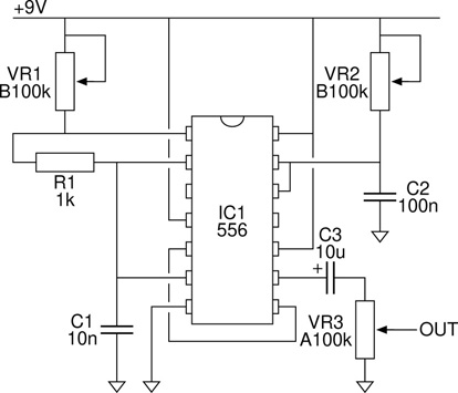
Figure 11.7 APC circuit diagram.
Notice that the frequency pots are specified as linear taper pots by way of the B designator in the circuit diagram. The output level pot, with an A designator, is indicated to have an audio or log taper. These niceties are not important to the operation of the circuit but can make for a more user friendly interaction characteristics as explained in the section on pot tapers in Chapter 12. It is always worth trying different pot variants in any circuit if the opportunity presents itself.
The final difference from the original design is that the orientation of the output capacitor is reversed. The original Forrest Mims design had the speaker referenced to the positive power rail (a somewhat unusual configuration) whereas the output jack here exhibits the more traditional ground referenced sleeve connection. It would be interesting to investigate if the symmetry of the output signal means that the originally specified mode of operation has any benefits or sonic differences.
As explained, the circuit is built around a commonly available IC called the 555 timer. The 555 timer itself is a very well known and much loved device popular with electronics hobbyists for the vast array of simple projects (audio and otherwise) which have been designed around it. The 556 chip specified in this project is just two 555 timers on one chip. The same project can also be found laid out for two individual 555 chips – the two alternatives are functionally identical.
The 555 timer itself is advertised as a high precision, high stability timing module which can be used to construct a variety of useful timer and oscillator circuits. Versatile circuits can be developed which can include such features as variable duty cycle and pulse width modulated square wave output signals. As is often the case, the chip’s data sheets provide guidance on how to design circuits for a wide range of applications, and as mentioned above the popularity of the device means that a vast range of other resources have been developed using the 555 timer in many and varied applications.
As mentioned already, the circuit here is built using a 556 chip which contains two individual timer blocks. The circuit uses the first timer to construct an oscillator. The output of this is then fed into the second timer which is configured to act as a variable frequency divider. The result is some very interesting sounds emanating from the circuit. It is difficult to convey visually the nature of the sounds available, which derive their primary character from the dynamic variations achieved as the controls are adjusted. The basic idea of the operation, and in particular the frequency dividing nature of the operation of timer two, can however be glimpsed in the traces shown in Figure 11.8. Channel 1 (top) shown the output of the first oscillator, whose frequency is controlled by pot VR1. This feeds into the second timer, whose output is displayed in the second trace. The frequency division aspect can be seen in the lower number of transitions present in trace two. The division factor changes in jumps as pot VR2 is adjusted giving surprisingly musical runs of ascending and descending tones.
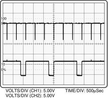
Figure 11.8 Output of the two oscillators in the APC.
The first of the two control pots varies the frequency of the initial oscillator while the second pot adjusts the frequency divider’s operation. The final control pot (VR3) is just a simple output level control. The waveform coming out of the chip will be too large for most signal inputs that it might be connected to, and so this pot provides whatever degree of attenuation might be required. Notice from the legend in Figure 11.8 that the display on each channel is set to five volts per channel and so it is clear that the output has an amplitude of about 7Vpk−pk.
Consider that the 386 amp in Project I has a maximum output swing of about 7V when run from a 9V battery, and that its minimum gain is 20. From this it is an easy matter to calculate the maximum peak-to-peak input signal level which the amplifier can handle without major clipping – Vpk−pk(max) = 7/20 = 0.35V. Clipping a signal which is primarily bi-level in nature such as that illustrated in Figure 11.8 makes little difference to its shape and thus its sound, but clearly the output of the APC is what could be called a hot signal, and an effective output attenuator is going to be a good idea.
Layout and Construction
As always the next step in the development of a project once a new circuit has been designed or otherwise procured is to come up with a good breadboard layout in order to test the basic design and also to test any modifications which might want to be considered. Figure 11.9 provides a layout for this project. The circuit itself is quite simple and as such an easy to follow design layout is not too taxing to arrive at.
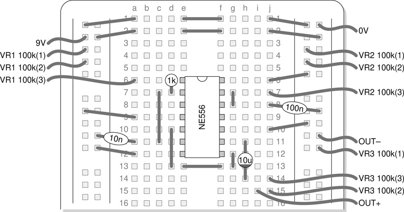
Figure 11.9 APC breadboard layout utilising an NE556 dual timer IC.
It would be good practice and most instructive for the reader to develop a layout from scratch. It need not turn out the same as the one provided here, indeed it is most unlikely to do so. The important thing is that it is (of course) correct but also organised and easy to follow. The designs included in this book sometimes include connections which might not seem the most obvious but are usually chosen in order to keep a neat and easy to read diagram, avoiding where possible crossing wires and component leads, and keeping connections short and in as much as it is possible, running vertically and horizontally. These details are not important to the operation of the unit, but can make the processes of building, testing, and debugging the actual circuit a far less painful experience.
Once satisfied with the results of the breadboard circuit the project can proceed on to the design of a suitable stripboard layout as shown in Figure 11.10, in order to allow for a permanent soldered circuit to be constructed. Often some of the physical layout can be derived from the existing breadboard layout, but the differing nature of the two constructions means that much of the layout will best be considered from scratch. It will often be the case that a couple of strips above or below an IC might best be designated as the primary positive and negative power rails for instance.

Figure 11.10 APC stripboard layout utilising an NE556 dual timer IC.
In this case with the two capacitors to ground emerging from pins close to the top of the chip it makes sense to have a ground strip at the top. Further consideration of the layout places the +9V bus at the bottom, as it becomes too crowded to get those connections up to the top as well. The second strip which has been used below the chip is perhaps a little wasteful of space. It is only used to make the connection between pins five and eight. This could have been achieved using a short jumper wire under (or indeed over) the chip. For the sake of clarity the extra strip was employed and the overall design remains compact.
Again the copper side of the board is shown in order to identify the correct locations for all the necessary breaks in the copper strips. This time it has been fitted to the side rather than underneath as in the previous project, and as such it must be remembered that positions are mirrored left to right rather than top to bottom as in the previous case. To reflect this difference notice that now the column numbers are inverted (1 to 12 becomes 12 to 1) while row letters (A to J) remain unchanged. Once again this maintains consistency when referencing locations on the board from either the component side or the copper side. Note for instance that column 6 runs directly under the chip on the components side, and on the copper side it hosts a column of breaks in the copper strips in order to remove the unwanted connections between the pins on each side of the chip.
It is always a worthwhile exercise to retrace the connections on the stripboard, remembering to take the breaks into account, and confirm that every connection corresponds to what is happening in the original circuit diagram. For instance, the break at 10J allows the negative terminal of the 10µF capacitor to connect to pin three of the output pot while separating this connection from the five +9V connections which come together on the rest of strip J. Similarly the break at 10A separates the final output connection from the ground bus which occupies the rest of this strip. Each point in the circuit can be similarly examined to confirm that the required connections, and only the required connections are being made. A useful technique when dealing with an integrated circuit is to go around each pin on the chip in turn and check that it goes to all the right places (and no wrong places).
The connection between pin two of VR3 and OUT+ at the top righthand corner of the board could be left out, and wired directly between the pot and the output jack. It has been included for clarity as this is intended to be a project suitable for a novice circuit builder. It is often the case that the wiring harness (all those connections to off-board components such as pots, switches, and jacks) is itself a complex affair and will regularly merit a separate set of build instructions dedicated specifically to getting it right.
Project III – Modulation Effect
Having built an amplifier and a noisemaker, project three presents an audio effect circuit. Effects take an audio signal as their input and they output an altered version of that signal. In the case of the modulation effect, how this signal alteration is achieved can in broad terms be described as follows. An oscillator modulates the state of a transistor in the audio path, and this produces a pulsating effect in the audio, which is heard as the ‘wobble’ which gave the original circuit its name – this particular project is based on a design called the ‘Wobbletron’, taken from a collection of interesting audio circuits generally referred to as ‘Escobedo’s Circuit Snippets’. The circuits in this collection were designed and annotated by Tim Escobedo and the collection has become one of the most popular sources of interesting circuit ideas for audio electronics hobbyists and experimenters. It is an excellent place to start for anyone interested in getting more deeply into practical audio electronics.
The circuit diagram for the modulation effect is shown in Figure 11.11. The only differences from the original design are that a value has been specified for C1, and the three transistors have been substituted (based on availability and using the substitution procedures outlined in Chapter 17). The circuit separates conveniently into two parts. To the bottom left can be seen the oscillator, while to the top right is the section which represents the audio path through the circuit. A single wire from the 500k pot VR2 to the gate of the JFET Q3 connects the two. This wire carries the oscillators output into the JFET, turning it off and on and thus wobbling the audio as it passes through this point in the circuit, producing the effect. It is worth noticing the circuit symbol used for the variable resistor VR1. This is a shorthand for the configuration seen for VR1 and VR2 in the APC circuit diagram shown in Figure 11.7. In the case of the APC the three connections to the pot terminals are shown explicitly. Here the diagonal arrow indicates a variable resistor but does not show exactly how to connect it. It is assumed in this case that the circuit builder will understand how to implement the appropriate wiring.
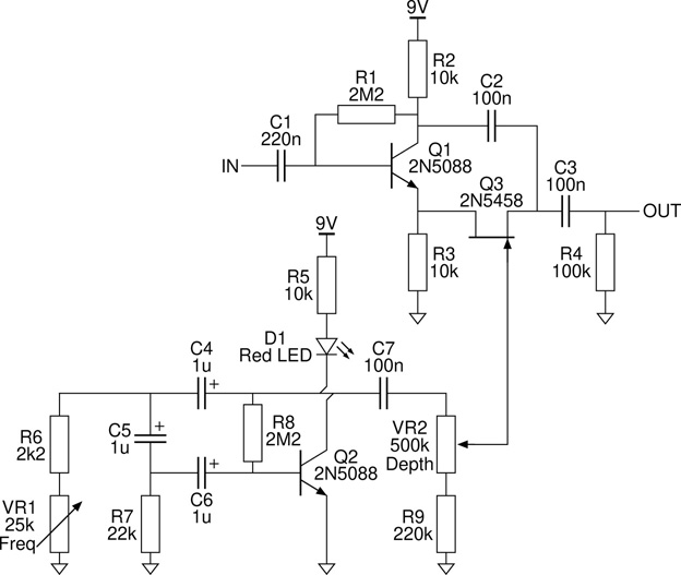
Figure 11.11 Modulation effect circuit diagram.
Circuit Operation
In electronics there are many ways to build an oscillator. This particular one is what is called a phase shift oscillator. When a signal passes through a capacitor it experiences a frequency dependant shift in its phase due to the lag introduced as the capacitor is charged and discharged. The amount of phase shift introduced is in fact a function of three things: the frequency of the signal, the capacitor’s size, and the values of surrounding resistors in the circuit. In this circuit a ring of three capacitors (C4, C5, and C6) can be seen to run from Q2’s collector to its base. Each capacitor introduces a little more phase shift to any signal passing along this route.
The transistor Q2 is connected in a common emitter configuration which is to say that its output is taken from the signal at the collector, which is an inverted version of the signal at the base. So if a particular frequency within this signal experiences 180° of phase shift in travelling through the three capacitors between the collector and base then when this is added to the natural 180° phase shift introduced through the transistor’s action that frequency will end up back in phase as it emerges from the transistor and as such will be amplified. Meanwhile all other frequencies which might have been present in the signal end up out of phase after travelling around this loop and therefore rather than reinforcing, these frequency components tend to cancel themselves out. In this fashion the initial random noise of the circuit kicks off self sustaining oscillations at a particular frequency while damping down all other frequencies.
Changing the setting of the 25kΩ pot VR1 alters the circuit conditions in the phase shift network and produces a different frequency with just the correct amount of phase shift to be reinforced. In this way a variable frequency LFO signal emerges from the oscillator ready to be applied to the gate of the JFET, driving the operation of the effect. With the component values shown the frequency range of the LFO typically runs from round about two hertz up to something in the vicinity of five hertz. This range can be quite variable from circuit to circuit due to component variability and can be adjusted in any particular case by selecting different values for the capacitors and resistors making up the phase shift network.
The LED provides visual feedback of the operation of the LFO as it flashes in time with the oscillator. This can prove to be quite a convenient first check when building and debugging this circuit as it immediately confirms whether or not this section of the circuit is operating. The flashing is likely to be quite dim as the LED is not driven hard, but it should be sufficient to be clearly visible in most cases.
Moving up to the audio section of the circuit, the audio signal which is to be affected enters the circuit at the point labelled IN. It then passes through the familiar coupling capacitor C1 and enters the base of transistor Q1. The three resistors R1, R2, and R3 set up the transistor’s operating point ensuring that suitable bias voltages appear at the various terminals of the device. Following the audio path as it continues on, signal is tapped off from both the collector and the emitter of Q1, the upper path via C2, a 100nF capacitor while the lower path is through the JFET Q3 whose state is being modulated under the control of the LFO. These two independently phase shifted signal components are recombined to yield the final modified signal which emerges from the circuit through the final output coupling capacitor C3.
Figure 11.12 illustrates the effect which this circuit has on an audio signal. Panel (a) shows the control signal emerging from the LFO on channel 1 while channel 2 shows the circuit’s modulating effect on the amplitude of an audio signal passing through it.
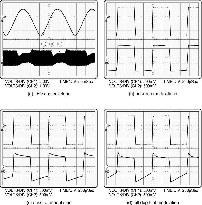
Figure 11.12 Operation of the modulation effect.
From the figures given in panel (a) the frequency of the LFO can be read off the plot as about five hertz, the top of the LFO’s range. The audio in the lower trace is at a frequency of approximately 1kHz which translates to about 500 cycles across the sweep of the plot. This is why the signal shows up as a solid black area – it is only the varying amplitude envelope which can be seen. On the other hand, panels (b) to (d), with a much quicker time base (seconds per division) allow the shape of the test signal to be seen. These three panels show the input and output signals at three different positions along the progress of the LFO modulation, labelled as points (I), (II), and (III) on the plot in panel (a). As can be seen, the input signal remains steady as it should, while the output signal goes from unaltered when the LFO level is sufficiently low to successively more heavily distorted moving into the centre of the wobble.
These plots were taken with the depth pot VR2 set close to maximum. As the depth setting is dialed back the amplitude of the signal going to the gate of the FET Q3 is progressively reduced. With the voltage swing driving the FET’s gate reduced the amount of modulation is reduced until finally there is not enough variation to modulate the signal at all. Thus the depth pot VR2 allows for control over the strength of the effect while the frequency pot VR1 alters the nature of the effect from a slow sweeping effect at low LFO rates to a strongly pulsating sound as the rate of the LFO increases.
Layout and Construction
The modulation effect is certainly the trickiest of the three project layouts presented here, but with a little effort a pair of breadboard and stripboard layouts which are both clear and compact can be achieved. When laying out transistors it is essential to know the exact part number which is to be used. A quick search online will offer up a data sheet for the device, and the ordering of the three pins can be confirmed. The pinout can differ from one part type to another, so it is important to confirm the correct ordering for the particular devices to be used.
Figure 11.13 provides the necessary information on the parts used in this case, and shows the correct pin designations. For the 2N5088s which are bipolar junction transistors Q1 and Q2 the pinout is shown as EBC, indicating that the pins are emitter, base, collector from left to right looking at the flat face of the device with legs down. For the 2N5458 JFET Q3, the DSG similarly stands for drain, source, gate, thus identifying the arrangement of pins in this device. Once all this is known, an appropriate circuit layout can be designed.
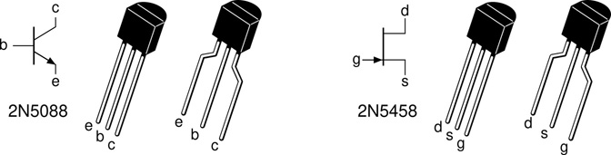
Figure 11.13 Pinouts for the transistors used in the modulation effect.
The separation of the circuit into two parts described above can be seen in the breadboard layout also around row 7 on the left and 10 on the right. Above these rows the audio section is laid out while below them is the LFO. With three transistors in the circuit, great care must be taken not to mix up the identical looking devices as they are inserted into the board, and it is of course also important to get the orientation correct. In this design the BJTs Q1 and Q2 on the left side of the board have their flat faces to the right, while JFET Q3 has its flat face to the left.
Notice also that the standard power rail connections have been included distributing 0V and +9V to both sides of the board. This has been done here as a standard step even though the +9V rail is not needed on the right side of the board and these three jumper wires across the top could be omitted.
Once again, having built a working circuit, it can be worth considering if any tests or modifications might be worth investigating. Reviewing the notes included in the original ‘Circuit Snippets’ document throws up a suggestion that the overall tone of the effect might be altered by trying different values for the input coupling capacitor. In fact the original circuit diagram does not specify any value at all. The 220nF size suggested here is simply a fairly typical value for this standard component. Larger values allow the full frequency range of the incoming audio signal to enter the circuit while smaller values will roll off progressively more and more of the low frequency components. As such, in common with many audio circuits, a lighter more trebly sound can be achieved using smaller input capacitor values while a fuller or darker tone can be achieved with larger values (assuming the original audio has significant low frequency components in the first place).

Figure 11.14 Modulation effect breadboard layout.
The characteristics of the LFO which is used to drive the modulation at the heart of this effect can also be altered. Changing the values of the three 1µF capacitors will alter the base frequency of the oscillations, while using a different size pot for VR1 will allows for a larger or smaller range of frequencies to be produced. As always, experiment, find the setup that gives the best results, and go with that.
With testing completed and design decisions finalised it is time to move on to the drafting of a stripboard layout. Again an example layout is presented here, in Figure 11.15 but it is always good practice to attempt to draft one from scratch. The layout given here is particularly busy and a less complicated one could certainly be developed if a larger stripboard matrix were used. While developing the smallest possible footprint can be a rewarding challenge, a more spread out stripboard design can make the building process much easier. This can be especially important until ones soldering skills have developed to the point where such tight quarters do not pose a problem in keeping solder joints safely separated.

Figure 11.15 Modulation effect stripboard layout.
The relatively large number and scattered nature of the breaks on the copper side of the board could also cause problems for a novice builder, in addition to the soldering of so many components at tight quarters. Given the regular 0.1 inch hole pitch of standard stripboard, it can be seen that this really will be a very small board, and aiming for a larger footprint might not be a bad thing for a first attempt at this project. With rows and columns of only six and sixteen respectively the board shown here will only be about half an inch high and one and a half inches wide. Not much room to play with but perhaps a good test of soldering skills.
References
C. Anderton. Electronic Projects for Musicians. Amsco Publications, 1992.
N. Boscorelli. The Stomp Box Cookbook. Guitar Project Books, 2nd edition, 1999.
B. Duncan. High Performance Audio Power Amplifiers. Newnes, 1996.
E. Evans, editor. Field Effect Transistors. Mullard, 1972.
W. Leach. Impedance compenstion networks for the lossy voice-coil inductance of loudspeaker drivers. Journal of the Audio Engineering Society, 52(4):358–365, 2004.
F. Mims. Engineer’s Mini-Notebook: 555 Timer IC Circuits. Radio Shack, 3rd edition, 1996.
R. Penfold. More Advanced Electronic Music Projects. Bernard Babani, 1986.
R. Penfold. Electronic Projects for Guitar. PC Publishing, 1992.
R. Penfold. Practical Electronic Musical Effects Units. Bernard Babani, 1994.
A. Sedra and K. Smith. Microelectronic Circuits. HRW, 2nd edition, 1987.
D. Self. Audio Power Amplifier Design. Focal Press, 6th edition, 2010.
G. Slone. High-Power Audio Amplifier Construction Manual. McGraw-Hill, 1999.
R. Wilson. Make: Analog Synthesizers. Maker Media, 2013.