3 | Semiconductors
The previous chapter concluded with a section about conductors and insulators. What is discussed there are materials at the two extreme ends of a continuum. In between them lie lots of substances that conduct electricity a bit but not really very well, things like water, graphite, people, and of interest here silicon and germanium. These latter two intermediate materials have some very specific and useful properties the details of which are unimportant but suffice it to say that they are called semiconductors and they are at the heart of all modern electronics. The one of most interest is silicon but germanium (which is only used a little today but which was much more commonly used in early semiconductors) are also mentioned briefly.
Pure Silicon
Silicon atoms form a nice regular lattice structure. As was stated in Table 2.1 this material will conduct a bit of electricity but really not very well at all. It offers quite a lot of resistance. Nonetheless if a pair of terminals are attached across a lump of pure silicon and an EMF is applied (remember, that is a voltage) some small amount of current would indeed flow. Reverse the EMF and the current would flow in the other direction. Attach the terminals on different sides of this little block of silicon and current flows just the same. So far nothing of any great interest or utility is happening. The silicon is acting just like a fairly poor metal, conducting electricity but not very well.
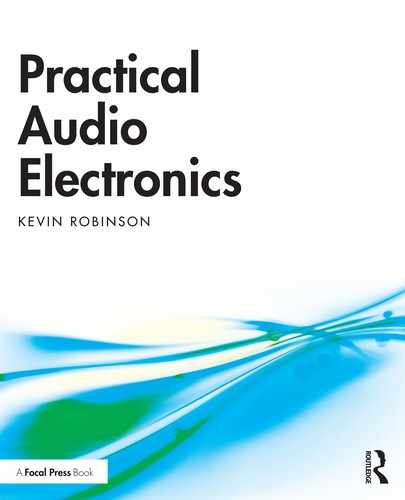
The main reason silicon does not conduct very well is that unlike metals it does not have any electrons which are free to move around easily. All its electrons tend to be bound up fairly tightly in the bonds that hold the silicon atoms together in its neat and tidy lattice structure, as illustrated in Figure 3.1. It takes a bit of energy to encourage electrons to abandon their positions and go roaming giving an electric current. So the first thing which is needed is to make it easier for electrons to move around a bit within the silicon’s crystal lattice. Two possible ways of doing this might be to introduce new less tightly bound electrons happy to move about or to provide new free locations that any nearby electron might feel inclined to move into and occupy.
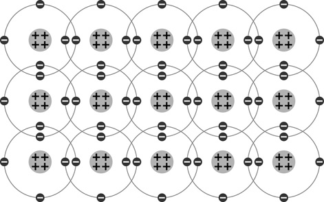
Figure 3.1 A crystal lattice of silicon atoms.
To arrive at useful semiconductor based devices it is actually necessary to do both of these things to produce two new types of semiconductor material called n-type and p-type. The ‘n’ in n-type stands for negative and this type of semiconductor has mobile electrons ready and able to move about. Likewise the ‘p’ in p-type stands for positive and this type of semiconductor has spare room which attracts wandering electrons. These electron friendly locations are usually referred to as holes. Each of these two new materials is much more conductive on its own than the original silicon was. Recall from Table 2.1 that pure silicon has a resistivity of around 640 · m. These new materials while still not nearly as conductive as copper will typically have resistivities tens of thousands of times lower than that of pure silicon. The exact resistivity depends on the concentration of these additional electrons and holes.
Doped Silicon
In order to achieve these new more conductive semiconductor materials take a nice well structured lump of silicon and swap some of the silicon atoms in the lattice for other elements. Do not worry too much about what they are, a few different elements can be used. The important thing is that these new elements have a structure similar to silicon but with different electron layouts providing either extra electrons or spare sites for electrons to fill (as previously mentioned these empty locations are called holes). This process of adding non-silicon atoms into the silicon lattice is called doping the silicon, and the other elements are called impurities or dopants. Dopant atoms are quite similar to silicon atoms so they fit into the lattice structure pretty well, see Figure 3.2.
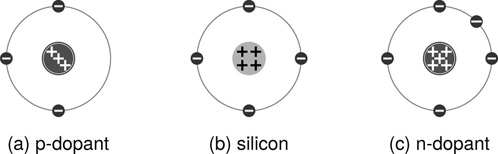
Figure 3.2 Simplified representation of silicon and dopant atoms. The p-type dopant atom is shown with one less available electron and correspondingly one less proton. In the n-type dopant an extra electron and proton are shown.
By adding some of these carefully chosen impurities some very useful behaviours can be achieved. What the impurities are doing is either adding a few extra electrons to the mix, or removing a few electrons from the mix (i.e. adding holes). When electrons are added the result is n-type semiconductor material, and when electrons are taken away the result is p-type semiconductor material. It is important to note that the materials stay neutral from a charge point of view because the impurities added have different numbers of protons to balance the different numbers of electrons present, Figure 3.3. Each of these two new materials on their own form fairly good electrical conductors as in both cases electrons are provided a mechanism for moving through the material easily, but still nothing very new and useful has yet been arrived at.
Figure 3.3 Lattices of p-type and n-type doped silicon.
The P-N Junction
Where it starts to get really useful is if a piece of p-type semiconductor and a piece of n-type semiconductor are placed side by side. This forms what is called a p-n junction at the interface between the two materials as in Figure 3.4. All along this junction there is a scattering of mobile electrons on the n-type side and a scattering of holes on the p-type side so unsurprisingly some of the mobile electrons migrate across the junction to fill nearby holes. The problem when they do this is that they leave behind their matching protons in the dopant atoms firmly fixed into the lattice structure. So as a result an electric charge builds up. The n-type side of the junction becomes positively charged (protons which have lost their matching electrons) and the p-type side of the junction becomes negatively charged (wandering electrons move into holes with no matching protons).
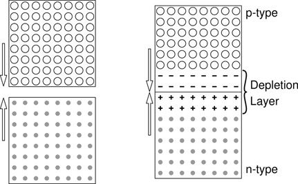
Figure 3.4 Creating a p-n junction.
The resulting electric field slows and eventually stops the migration of electrons across the junction. Remember that opposite charges attract and like charges repel so the increasing negative charge on the p-type side of the junction discourages the migration of further (negatively charged) electrons, while on the n-type side the increasing positive charge tends to encourage the remaining electrons to stay where they are. An equilibrium state is achieved where the effect of the electric field counters the tendency of electrons to move across the junction to fill the waiting holes. The region close to the p-n junction where electrons have abandoned their original positions and filled nearby holes across the junction is referred to as the depletion layer or depletion zone, so called because the available charge carriers (mobile electrons and vacant holes) in the region have been depleted. In a typical p-n junction made from silicon based semiconductors the corresponding build-up of positive and negative charge results in a potential difference of round about 0.6V appearing across the junction.
Now all that has been described so far has happened with the semiconductor materials just sitting on the bench. No electronic circuits have been built and no external electric voltages have been applied. It was observed previously that both n-type and p-type materials were fairly good conductors in their own rights so the question now becomes how good a conductor is this new p-n junction structure going to be? And finally the point has been reached where something useful happens, because the answer to that question is, it depends on the direction in which the external voltage is applied. Consider taking a battery and attaching wires from its terminals to either side of the p-n junction. The results will depend on which side of the junction is connected to the positive side of the battery and which to the negative. Consider each case in turn.
Reverse Biased P-N Junction
Imagine a p-n junction with a battery attached as shown in Figure 3.5 with its positive terminal attached to the n-type material and its negative terminal attached to the p-type material. In this configuration the battery’s voltage is applied in the same direction as the internally generated voltage already sustaining the nonconducting depletion layer. This new external voltage therefore causes the depletion layer to widen. Thus in this situation no current can flow in the circuit because electrons have no way of flowing across the depletion layer. This is called reverse biasing the p-n junction.
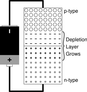
Figure 3.5 Reverse biased p-n junction.
Forward Biased P-N Junction
Now take the same circuit and reverse the connections to the battery so that the battery’s voltage is now applied in the other direction across the p-n junction. The depletion layer now starts narrowing as the applied voltage from the battery overcomes the induced voltage generated by the original migration of charged particles across the junction, Figure 3.6. Once the voltage being supplied by the battery exceeds the internally induced voltage (at round about 0.6V for a typical silicon based p-n junction) current can flow through each piece of semiconductor material just as if the other were not there. This is called forward biasing the p-n junction.
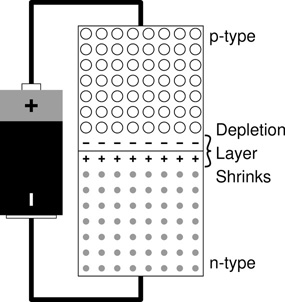
Figure 3.6 Forward biased p-n junction.
This behaviour leads to the ability to control whether current flows or not depending on the direction of the applied voltage. It makes the p-n junction a very useful structure and is the basis of many and varied electronic components. The operation of some of the most important of these are examined briefly in the next section. This is just intended to give an idea of how things work without looking at real world circuits or applications. Later the much more practical question of how they are used and what can be done with them is addressed.
Diodes and Transistors
The two most important classes of components which utilise the semiconductor materials just introduced are diodes and transistors. Later chapters talk about how to employ these components in various useful ways, but before looking at the purely practical questions of application and performance it will be useful to develop a general understanding of how these important components actually function in order to achieve the various kinds of circuit operation for which they are employed. While a deep understanding of what is going on inside these components is entirely unnecessary a more basic appreciation of what is happening will assist greatly in designing and understanding the circuits to be encountered throughout this book.
Diodes
The simplest semiconductor based device is the diode, and this has already been described in as much detail as is needed. A basic diode is exactly a p-n junction and nothing more and all that has just been said above regarding p-n junctions applies to these very simple devices. The simplest analysis of a diode says that a diode allows current to flow in one direction but not the other. For many applications this is all that is needed.
It was mentioned that the forward bias voltage needs to exceed about 0.6V before a typical p-n junction will start to conduct so the simple analysis is a bit too simple for some cases. This turn on voltage is often used to advantage in audio circuits. For example a very rudimentary fuzz type electric guitar effect can be achieved using little more than one or two diodes. The fuzz distortion is achieved as a result of the audio signal only passing through the diode when the signal’s level exceeds the turn on voltage of the diode. This is seen in action later.
There are in fact many different types of diode, some are just slight variations on the basic component described here while others are vastly different in the details of their structure and performance. Most of these are of absolutely no interest here but there are a couple which are likely to be encountered. The most common of these are the light emitting diode (LED), the Zener diode, and the Schottky diode.
LEDs just generate light as a byproduct of the operation of the p-n junction. Apart from this point and the fact that their turn on voltage is a bit higher they are no different from ordinary diodes.
Zener diodes can at first seem a little strange in the way they operate. The standard diode considered so far does not conduct any significant amount of current when reverse biased. However if the reverse bias voltage is increased enough then (as with most things) eventually the diode breaks down and starts conducting strongly. For a normal diode this should happen at a voltage well above anything which will be seen in the circuit because when it happens to a standard diode the component is likely to be destroyed. Zener diodes on the other hand are specifically designed to be operated at this breakdown point and they are in fact used to provide stable voltage references within a circuit because the voltage at which they breakdown can be chosen quite accurately when they are manufactured. So for instance a 6.3V Zener diode is designed to provide a very stable and reliable six point three volts across its terminals when reverse biased. Simple voltage references of this kind are very useful in many circuits.
The Schottky diode is very similar in function to a standard diode except that it exhibits a lower switch on voltage and faster switching, but it also has a higher reverse bias leakage current.
All these aspects of diode behaviour are returned to later when these components are actually utilised in various circuits. Then the significance of the different variations in their behaviours can be appreciated more fully.
Transistors
Transistors are a much more complex subject area than are diodes. There are many different types all with their own special characteristics and areas of application but at the heart of each one still lies some variation on the basic p-n junction examined above. Fortunately once again only a fairly small subset of the large variety available are of interest here. The array can still be a little overwhelming to begin with however. They are introduced here in an orderly fashion so that it is a little easier to keep organised and clear. Figure 3.7 shows how the major types can be broken down.

Figure 3.7 The major transistor types.
To start with remember that there are four different types and each type has a positive and a negative variant. The first split is between bipolar junction transistors (BJTs) and field effect transistors (FETs). There are the positive and negative BJT variants called NPN BJTs and PNP BJTs, and that is it for that side of the tree. The FET side gets further broken down into JFETs and MOSFETs, and then MOSFETS get broken down again into normally off and normally on types. Each of the three types of FET comes in n-channel and p-channel flavours. In fact the vast majority of all the transistors likely to be encountered working in audio electronics fall into just two of these eight categories: NPN BJTs and n-channel JFETs.
Whatever the type or variant in question, the basic idea of a transistor remains the same. A transistor has three terminals (as compared to a diode’s two) and one way or another what happens at one of those terminals controls the behaviour between the other two. Transistors can operate as switches, buffers, and amplifiers. These are their three basic roles in all the circuits in which they appear throughout this book.
The BJT (bipolar junction transistor) looks a little similar in structure to the diodes already considered. All that is needed is to add another layer of semiconductor material to the stack as in Figure 3.8. Adding another piece of n-type semiconductor gives an NPN BJT and adding another piece of p-type semiconductor gives a PNP BJT.

Figure 3.8 The structure of NPN and PNP bipolar junction transistors.
The three terminals of a BJT are called the base (B), collector (C), and emitter (E). The base is the one that does the controlling while the other two are controlled. Since a BJT is essentially two p-n junctions facing in opposite directions it might seem that a BJT should never conduct between the collector and the emitter as one of the two junctions will always be reverse biased, but of course it is a little more complex than this. By altering the voltage on the base terminal which is connected to the central semiconductor layer, the conductivity of the path between the collector and the emitter can be controlled. The details of how this works are not important once the principle is grasped.
The JFET or junction field effect transistor has a somewhat different structure from the BJT (Figure 3.9). Its three terminals are also given different names to those given to the BJT’s terminals. In this case they are called the gate (G), drain (D), and source (S). These names remain the same for all FETs. The structure of the JFET can be thought of as a single channel of one type of semiconductor material which runs all the way from the drain at one end to the source at the other and the control terminal (the gate) is attached to a region of the other type of semiconductor material which surrounds the channel. The idea in this case is that when a voltage is applied to the gate it can induce the same kind of depletion region as seen in a reverse biased diode. When this depletion layer extends all the way across the channel, conduction is prevented and the transistor is said to be cut off. Reversing the voltage on the gate causes the depletion region to retreat allowing the channel to conduct once again.
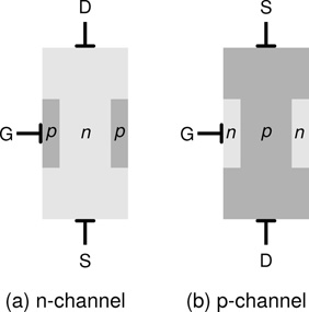
Figure 3.9 The structure of n-channel and p-channel junction field effect transistors.
So the name explains fairly well how a JFET is made and how it works. The ‘J’ for junction indicates that there is a p-n junction involved and the field effect bit refers to the electric field which spreads out from the gate junction opening and closing the channel. So the terminals are well named too: the gate controls the flow, and the other two terminals, the drain and source are where the main current flows into and out of the device respectively.
The MOSFET is even more explicit in its name as to the structure of the device. The MOS stands for metal oxide semiconductor which are the three layers involved in making one of these types of transistors as seen in Figure 3.10 and the FET half of the name stands for field effect transistor as before. In this case the oxide layer insulates the gate from the channel so that, while the electric field can still extend out from the gate, opening and closing the channel, no actual current can flow into or out of the gate terminal. In other words the gate terminal has an extremely high input impedance, which can be a useful attribute in certain circuit design situations.
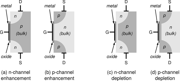
Figure 3.10 The structure of n-channel and p-channel enhancement mode (normally off) and depletion mode (normally on) metal oxide semiconductor field effect transistors (MOSFETs).
Although the technical details are very different, in terms of operation the MOSFET can be considered as working in a similar fashion to the JFET. Put simply a voltage applied to the gate is used to control the flow of current through the channel between the drain and source terminals. As the voltage on the gate is changed in one direction the electric field extends further into the body of the device (labelled bulk in the figures) causing the channel to retreat back towards the regions around the drain and source terminals. And as the voltage on the gate is changed in the other direction the electric field reverses and the conductive channel is encouraged to extend back out linking the drain and source and allowing more current to flow.
The only real difference between the enhancement mode (normally off) MOSFET and the depletion mode (normally on) MOSFET is as the names in brackets imply the first type has no conduction between drain and source when the gate voltage is held at zero volts whereas in the second type the drain source channel does conduct at zero gate voltage. So in the case of the depletion mode MOSFET the voltage on the gate has to swing further in the off direction in order to turn the transistor fully off. Which direction is off depends on whether it is an n-channel or a p-channel device.
Figure 3.10 illustrates these behaviours. No channel is present by default in the enhancement mode type which therefore is normally off. In the normally on depletion mode type on the other hand a channel is shown as being present by default. This is a good way of visualising and remembering the behaviours of these different types of MOSFET.
Germanium Semiconductors
Most semiconductors these days are based on the element silicon. However there was a time when many were manufactured using germanium as the base material rather than silicon. For most purposes germanium devices operate in fundamentally the same way but germanium makes rather poorer semiconductor components than does silicon. A bit more current leaks through the p-n junction under reverse bias conditions. Switching between on and off states tends to be slower and less well defined. In fact germanium generally exhibits poorer performance all round. Germanium diodes do however start to turn on at a lower voltage (typically round about 0.3V) and so they often find favour where very small signals are being handled in homemade radio receivers and such like. They are also used in many audio circuits where their somewhat slower and more gentle approach to switching can lead to subjectively more pleasing results when working with audio signals.
Germanium diodes and transistors are becoming increasingly scarce and difficult to source and correspondingly more expensive. There is however still a significant demand for the components in the niche audio electronics area. Along with vacuum tubes, germanium components hold a special place in the world of audio electronics as components which have been superseded and replaced elsewhere but still have a role to play due to their particular characteristics and how they affect the audio signals which pass through them. Some of this is undoubtedly unfounded or exaggerated but there are places where their special character does make a real (if subjective) difference to the performance of an audio circuit.
References
E. Evans, editor. Field Effect Transistors. Mullard, 1972.
A. Sedra and K. Smith. Microelectronic Circuits. Oxford University Press, 7th edition, 2014.