
7 | Circuit Diagrams
Circuit diagrams in the broad sense can cover a wide range of different circuit or system representations. At the most abstract, block diagrams can be used to conceptualise the high level functional blocks in a system, and the connections and signal flow between these blocks. Such representations may be referred to as block diagrams, functional block diagrams, signal flow diagrams, connection diagrams, etc. Moving to a more detailed design, the schematic diagram includes full details of which components are actually required in order to build the circuit in question, and the precise connections between all these components. Circuit schematics or schematic diagrams are often also referred to simply as circuit diagrams, and when this term is encountered in a general context, this kind of diagram is usually what it is being used to refer to. A schematic diagram defines how a circuit is to work, but does not provide a full blueprint to building it. The third and final class of circuit diagram adds physical layout information to the mix in the form of a breadboard, stripboard, or printed circuit board (PCB) layout diagram. These provide a representation which can be directly followed by a builder in order to construct the circuit, and are the usual end product of the initial circuit design process, before building, testing, and modification commences.
Block Diagrams
Block diagrams can be a very useful tool in the early stages of the design process, allowing for the general architecture of a circuit to be analysed and assessed. They are also often employed in order to provide a high level description of an existing system to users, who do not need a detailed understanding of the inner workings of the system but only require a firm grasp of the general operation, the options and controls available, and what connections and setup are required or optionally available. Block diagrams are useful when explaining a circuit to a new user. They can also be used to help guide the construction, servicing, or repair of larger systems which might be composed of multiple physical circuit boards and ancillary connections to other devices. Figure 7.1 illustrates the typical functional blocks and signal flow in a simple synthesiser. It clearly differentiates between different kinds of control signals and audio signals, and indicates the major controls and options available in each section of the device.
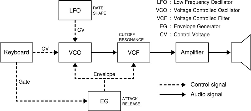
Figure 7.1 A typical block diagram.
Functional block diagrams and signal flow diagrams, although useful, are not usually required for the relatively simple kinds of circuits which are the main focus of this book. Additionally, such diagrams are generally relatively straightforward and self explanatory in structure and interpretation, and as such require little more in the way of explanation or examination here.
Schematic Diagrams
More often than not a project starts out with a schematic diagram. The correct and unambiguous interpretation of such diagrams is essential if a circuit is to be successfully constructed. The component symbols introduced in Chapter 6, along with the broader collection presented in Appendix C, and still more symbols and variations in common use generally, form the core of the schematic diagram representations which must be recognised and interpreted. Many additional conventions are gathered around these basic symbols in order to provide a comprehensive and (relatively) consistent methodology for the schematic representation of electronic circuit designs. Often some amount of creative license is employed by the drafter of a schematic diagram, but once the reader has gained a moderate amount of familiarity with the general conventions, interpreting the intended meaning is usually a straightforward matter. Occasionally a bit of research or experimentation may be needed if a schematic has been drafted without sufficient attention to detail, but on the whole this is rare.
The simple circuit introduced in pictographic form in Chapter 2, and reproduced here in Figure 7.2a, can be drawn in a more formal fashion as shown in Figure 7.2b. Once the two symbols used to represent the battery and the bulb are known, this schematic representation of the circuit should be easily interpreted. All the information needed in order to build the circuit is presented. Notice in particular that some components, such as the bulb here, have connection points or terminals which are interchangeable. It does not matter which way round such a component is connected into a circuit. In other components (such as the battery here) the terminals must be differentiated. The positive and negative terminals of the battery are not generally interchangeable in a circuit. Although in this particular case the battery connections could be flipped without altering the circuit this is not generally the case and the orientation of such components in a circuit must be carefully observed.
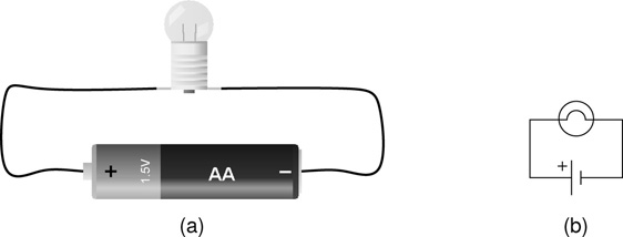
Figure 7.2 Pictographic versus schematic representation of circuit.
Schematic Layout Conventions
As the circuits being represented get bigger and more complex it is important to make sure that the schematic diagrams drafted to represent them are as clear and consistent as possible. A number of conventions exist which can help in this respect. Ignoring such conventions does not alter the accuracy of the schematic diagrams, it just results in schematics which are less easily followed and interpreted. Oftentimes it is not possible to follow the conventions strictly, but by and large the more closely they are observed, the easier the tasks of drafting and of reading the schematic become.
The most broadly applicable conventions guide the overall layout of the diagram. Inputs are on the left, outputs are on the right, and signals travel left to right through the circuit. This is not always strictly possible, but in general applying this convention makes it much easier to follow the signal flow in a complex circuit. The second, related convention stipulates that the power supply voltages generally go from positive to negative moving from top to bottom within the schematic diagram. Very commonly for simple circuits, perhaps powered from a single nine volt battery, a line across the top of the diagram connects to the positive terminal of the battery, with a similar line along the bottom connecting to the negative terminal. Finally, components and the traces connecting them are, in as much as it is possible, laid out horizontally and vertically. These three general points are illustrated in the circuit represented in Figure 7.3.
Figure 7.3 Schematic for a simple booster circuit, illustrating conventional positioning and routing of inputs, outputs, and power connections. Inputs enter from the left. Outputs exit to the right. Positive power supply voltages enter from the top and negative voltages connect from the bottom. This circuit is revisited in Chapter 17.
Power connections can in fact be represented in a number of different ways. The simple circuit in Figure 7.2b explicitly places a battery rather than incorporating the power rails as described above. Several options are illustrated in Figure 7.4. The first three contain some implicit suggestion as to what the intended power source is. The first two are a battery and a power jack for connection of an external PSU. The third indicates a general DC source and is suggestive of the kind of adjustable bench power supply found in an electronics lab. The final pair – which utilise labelled power terminals, symbolic ground points, and power rails – make no such suggestions and are entirely generic.

Figure 7.4 Various alternative representations of power connections.
While there may be good reason in a particular case to specify for instance a battery or a power adapter, such choices can generally be assessed and finalised when the circuit is actually being built. The abstract power supply variants carry no direct implications and are by and large interchangeable, their choice being based on questions of convenience and clarity.
Sometimes particular power connections are not explicitly shown in a schematic diagram at all. The drafter of the schematic is in this case assuming that the builder knows that certain power connections are needed in order to complete the circuit. Opamps and other ICs are commonly included without power connections being shown. Figure 7.5 shows equivalent opamp subcircuits. In the first case the power supply connections are explicitly shown, while in the second the connections are assumed. There is no difference between the circuits being represented by these two alternative diagrams.

Figure 7.5 Opamp power connections may or may not be shown.
A dual opamp is a commonly found eight pin DIP IC. It contains two totally separate opamp circuits, with just a single pair of +/− power connections serving both. When such a device is used in a circuit, often one of the pair of opamps will be represented with a symbol which includes the power connections, while the second opamp will omit these connections. The same situation pertains in the realm of vacuum tubes, where one of the commonest tube types still in use today is the dual triode – a single physical tube containing two triode valves. Valves require a heater in order to work, but often a single pair of +/− connections will supply the heaters for both valves. As such, a circuit diagram using one of these tubes will often include the heater connections with the symbol for one of the valves, while leaving the second valve without. It is even occasionally the case that one of the two connections is shown on each of the two valve symbols (Figure 7.6).
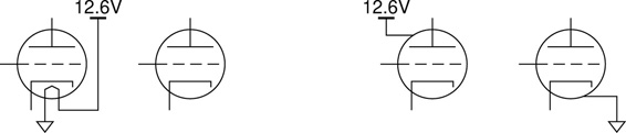
Figure 7.6 Vacuum tube heater connections.
Input and output connectors can be similarly implicitly or explicitly represented on a schematic diagram (Figure 7.7). At the simplest level, a line labelled, for instance, IN might be all that appears. Alternatively, a more explicit TS jack symbol might be used. In this case the tip (T) portion is connected to the line carrying the signal into (or out of) the circuit. The sleeve (S) portion may be left undecorated, or it may have an explicit connection to signal ground indicated. All these representations correspond to exactly the same final circuit connections. When not shown explicitly, it is assumed that the necessary ground connection is understood.
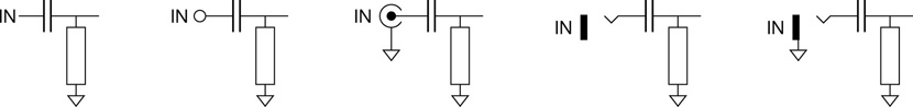
Figure 7.7 Input and output jacks can be represented at varying levels of detail. All of the above might be encountered, representing the same connections on the final circuit.
Generic Components and Component Substitutions
There are often various alternatives which may be substituted for a particular component without affecting the performance of the circuit to any significant degree. Transistors and diodes are the two component types most commonly subject to these kinds of flexible circuit diagram representation. Diodes will often simply be labelled Si for silicon or (less commonly) Ge for germanium, indicating that most typical diodes made from the specified material may be used. Similarly, transistors can be labelled with something like ‘any high gain NPN’. Many years ago Elektor magazine instituted a system whereby noncritical diodes and transistors in the circuits they published would be labelled DUS, DUG, TUN, or TUP as appropriate (see Table 7.1) rather than specifying particular part numbers for the components to use (Elektor, 1974).
| Acronym | Meaning |
| DUS | Diode Universal Silicon |
| DUG | Diode Universal Germanium |
| TUN | Transistor Universal NPN |
| TUP | Transistor Universal PNP |
The magazine article included details of the minimum allowable specifications for diodes and transistors to qualify as suitable devices to use in such situations. These details are reproduced here in Table 7.2 and Table 7.3. Also included in the original Elektor article were lists of commonly available devices which fitted into each of the four specified categories. While this system is not in common usage today it is still encountered occasionally, and in any case it does provide a very useful illustration of how to approach the more general question of identifying suitable substitute components for specified devices which are not readily available to the circuit builder.
| Type | VR max | IF max | IR max | Ptot max | CD max | |
| DUS | Si | ≥25V | ≥100mA | ≤1µA | ≥250mW | ≤5pF |
| DUG | Ge | ≥20V | ≥35mA | ≤100µA | ≥250mW | ≤10pF |
Table 7.3 TUN and TUP transistor specifications
| Type | Vceo max | Ic max | hfe min | Ptot max | fT min | |
| TUN | NPN | ≥20V | ≥100mA | ≥100 | ≥100mW | ≥100MHz |
| TUP | PNP | ≥20V | ≥100mA | ≥100 | ≥100mW | ≥100MHz |
Notice that the values in all but two of the numerical categories across the two tables are marked ≥, with just the values in IR max and CD max labelled ≤. This is separate from and not to be confused with the min and max designations in the column headings. Thus in the second table Ic max and hfe min are both quoted as ≥ values, indicating that both specifications should have values greater than or equal to the quoted levels. The only two specifications quoted here where lower is better are a diode’s maximum reverse leakage current (IR max) and its total capacitance (CD max).
General Schematic Diagram Labelling, Markup, and Organisation
A few other commonly encountered conventions are also worth mentioning. When a device (such as the dual opamp or dual triode tube mentioned above) consists of two or more sections within the same device, the different sections may appear in different parts of a circuit far removed from each other within the layout. In this case it is standard practice to label the sections with the same initial label and to append an a, b, c etc. in order to indicate the association between the otherwise unconnected parts of the diagram (notice the labelling of the two opamps in Figure 7.16). This practice is also commonly encountered with multi-pole switches (see Chapter 15) and various types of integrated circuits in addition to dual opamps. For instance the individual gates in a quad XOR or a hex NOT IC (see the 4000 series chips described in Chapter 18) are often scattered throughout a circuit, and labelled appropriately in order to indicate their common physical location.
As previously mentioned, power and ground connections are often individually labelled in order to avoid tracing lines all around a complex circuit diagram making it much more difficult to read. Other points can be similarly labelled for the same reason. One common example is a generated mid voltage levels (see the points labelled +4V5 in Figure 7.16), or other reference voltage (often designated Vref). In fact any difficult to route connection may be omitted, simply labelling its two ends instead (see the two points labelled A, also in Figure 7.16). This approach should not be used too frequently or the resultant scattering of labels quickly becomes even more difficult to follow than the snaking lines which they replace would have been.
A large circuit can also be broken into convenient subcircuits, with the points at which they interconnect similarly labelled. In Figure 7.16 a small section has been hived off and placed to the right of the main circuit, separated from it by a dashed line. Small sections of power supply circuitry like this are often drawn in isolation, in order to keep the overall layout as tidy and uncluttered as possible. Larger circuits will by necessity be broken up across several pages, but the magnitude of projects considered in this book will usually fit comfortably on a page. The noise gate example which rounds out this chapter is around the top end of the size of circuits likely to be encountered until a significant amount of experience has already been gained in practical audio circuit building.
A clear and unambiguous differentiation must be maintained between crossing lines which represent four wires connecting together at a point, and crossing lines which simply intersect in the diagram on their ways to their respective destinations. Leaving such a crossing point undecorated is very bad practice, although this can be encountered. Sometimes it is intended to mean that there is a connection at this point and sometimes not. It is usually obvious from the wider context of the circuit, but it introduces an unnecessary and highly undesirable level of uncertainty. Table 7.4 illustrates some common conventions used to indicate these two situations in schematic diagrams. The schematics in this book adopt the first pair as their standard representation of these two situations.
| Connected | Unconnected | Ambiguous |
In fact it is good practice wherever possible to avoid bringing four connected wires together at a point. Introducing a small offset wherever possible can help to remove any doubt or confusion. Both sides of resistor R11 in Figure 7.16 feature unambiguous four point connections. (In fact to the right of R11 is actually a six way connection since point A leads to another three components at its far end.) For comparison, the point to the right of R8 in the same diagram illustrates a usage of the first connected wires convention illustrated below. See also Figure 11.7 for several examples of unconnected crossing lines.
Integrated Circuit Representations
ICs can be represented on a schematic diagram in a number of different ways. The most direct representation for a DIP IC consists of an outline of the physical chip with its two rows of legs showing the connections to be made to each. Alternatively, a simple box can be used with connections entering at whatever points are most convenient. In this case each connection must be accompanied by a corresponding pin number in order to specify where on the chip the connection is to be made.
For some types of IC (opamps being the most obvious case, but also including logic gates, and some other specific IC types), special symbols have been adopted in order to represent the functions performed by that particular chip. Some of these are included in the table in Appendix C. Figure 7.8 shows examples of the three alternative styles of IC representation.
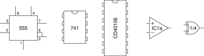
Figure 7.8 Different schematic representations for ICs.
Standard Omissions
A number of instances have already been mentioned where omissions are made, on the assumption that the builder will know to add these connections in the final circuit. Power and ground connections, including the sleeve connections of input and output jacks, have been discussed. A few other standard circuit elements are also commonly omitted or left up to the builder’s discretion. A circuit may be battery powered or it may take its power from an AC adapter, or it might be deemed desirable to allow for either option. In this latter case the usual arrangement will mean that any battery present will be disconnected if a jack is inserted into the power socket. This requires the use of a switching socket for the AC adapter, appropriately wired. Such details are rarely included in the schematic for the kind of generic audio circuit targeted here. A TRS jack at the input can often be found in guitar effects pedals, wired up to perform the function of an on/off switch. The details of implementing this, along with other options mentioned here, are covered in the standard building blocks discussed in Chapter 15.
More involved powering options are also available. Reverse polarity protection can be valuable when sensitive circuitry is involved. More elaborate transient protection is also possible, although this kind of advanced protection is more likely to be found on expensive equipment than on the kind of low end projects which are the primary focus here. The added cost and complexity is simply not justified in the case of smaller, less expensive circuits and projects. Such circuity may occasionally be encountered however, and so it is worth being aware of its existence.
It can also sometimes be beneficial to apply some tidying up to a circuit, which again is not usually shown on the circuit schematic. If a multi-section IC is used, such as one of the quad XOR or hex NOT 4000 series ICs mentioned earlier, it is quite likely that not all sections will end up being used. In this case it can be worth while terminating the unused sections so as to minimise the chances of noise or oscillations being generated, or unregulated current draw diminishing battery life. A good rule of thumb to start with is to tie unused inputs to ground, and leave unused outputs floating. This is not a universal approach but it is a good start in the absence of any other guidance. (Manufacturer data sheets sometimes offer advice in this regard.) Often a mid-level Vref voltage rail is a better place to tie the inputs in a circuit with a single rail power supply. For instance, unused opamps in a dual or quad package are probably best wired as a voltage follower, as shown in Figure 7.9, with IN+ wired to Vref and OUT wired back to IN–. This keeps everything sitting nice and steady at the reference voltage (ideally half way between the power rails), preventing oscillations and minimising current draw.
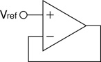
Figure 7.9 Wiring unused opamp sections.
Audio effects circuits will typically require a bypass option so that they can be switched in and out of the signal path. Such bypass wiring may or may not be shown, but in any case it is always an option as to whether and how to implement it. Alternative schemes, along with their advantages and disadvantages are also covered in Chapter 15. One of the variants presented includes a status LED in order to indicate what state the bypass switch is in. Such status LEDs, along with power indicator LEDs are often desirable but seldom included explicitly on a schematic. The choice of whether and how to add them is always available, and such decisions are best not left until the end of the circuit layout design phase which is described next.
Breadboard Layouts
Laying out a circuit, whether on breadboard, stripboard, or printed circuit board (PCB), is as much an art as a science. Practice, experimentation, patience, and attention to detail are the best route to generating a successful layout. The PCB option is a more advanced approach to circuit building and is not covered here, but some guidance towards the drafting and interpretation of breadboard and stripboard layouts is provided. Layouts are produced using symbols which broadly reflect the physical form factors of the various components to be used in the final construction, rather than the abstract symbols encountered previously in schematic diagrams. These layouts, unlike a schematic diagram, are direct physical representations of the actual circuit to be constructed. As such there is less scope for interpretation, and thus less use for abstract drawing conventions. The layout of complex commercial circuit designs is an extremely involved business. Often many factors need to be taken into account; noise, interference, high frequency performance, accuracy and precision, size and shape of the circuit board, heat dissipation and power management, and numerous other considerations can all feed into the design process. The audio circuits being considered here require little of this level of detail in order to arrive at an effective and efficient final circuit layout. Indeed the breadboard and stripboard circuit building options do not lend themselves to such exacting standards in their design requirements. Even the next step up, simple single sided PCB circuit layouts, provide only limited flexibility in this regard. Professional multilayer designs where these considerations come into play are far beyond the scope of what is presented or required here.
Breadboards enable simple plug and play circuit construction. Components can be added and removed without the need for soldering or otherwise fixing the connection points. They provide an excellent framework for experimentation and testing. The downside is that breadboard based circuits are not robust. Components can work loose, and wires can move around and touch, making unwanted, possibly intermittent, connections. As such they can be difficult to debug if sufficient care is not taken in their construction, and they are entirely unsuitable for permanent projects. Breadboards are for prototyping, learning, and experimenting; once a circuit is finalised, a soldered version is the best option for a permanent build. This entire procedure is examined in Chapter 10 – Constructing Circuits.
Breadboards come in various shapes and sizes, but by far the most common format is laid out as illustrated in Figure 7.10. Each numbered row in the centre of the board consists of five connected insertion points, allowing for up to five components to be connected together by inserting legs and wires into the five holes. The gap down the middle of the board is just the right size for a DIP IC (as introduced in the component list in Chapter 6) to span the central reservation. Four longer busses run vertically from top to bottom, two on each side of the board. There will usually be a gap about every five steps along these busses but the connection runs all the way from one end to the other. These busses are most commonly used to connect power into the board, but there is nothing special about them and they can in fact be used for any connections (in Figure 7.17 the first of the four busses is used to facilitate a tricky set of intra-circuit connections, while the other three are used in their more familiar roles, two providing board-wide connections to 0V and the fourth connecting to +9V).

Figure 7.10 A blank breadboard template, ready for populating.
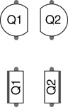
Symbols like those illustrated in Table 7.5 can be used to design a layout for a circuit. Attempting to go straight from a schematic diagram to building a physical breadboard version of the circuit is likely to prove a very frustrating endeavour. Things will quickly become confusing and difficult to follow. Much better to first design a layout by drafting a diagram, as described here. The actual building process is then a simple matter of copying the finalised design onto the actual breadboard. The symbols presented here are not standard representations, but rather just aim to be graphically recognisable as, and with a comparable footprint to, the actual components they are intended to indicate. This table includes only on-board components. Off-board components such as jacks, pots, and switches are represented only by the flylead wires going to their connection terminals. This is the style preferred here. Others may choose to include graphical elements to represent off-board components also.
Table 7.5 Circuit layout component symbols used in this book
Name |
Symbol |
Description |
Resistors |
|
In common with their schematic diagram symbol, resistors are mostly represented here on breadboard and stripboard layouts by a simple rectangle. When a layout requires the two leads to be placed very close together the rectangle symbol no longer works well, and instead a circle is centred over one of the connection points with a lead extending to the other, nearby point. The idea is to represent the resistor as if it were standing on end with its top lead bent down through 180° in order to make the second connection. In a tight layout this is often what is actually done in order to reduce the footprint of resistors and other axially leaded components. |
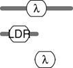
Photoresistors (aka light dependant resistors, LDRs) |
|
The shape of the photoresistor’s symbol reflects the shape of the type of LDR most commonly encountered (see Figure 12.16). The Greek lambda is a symbol often used to designate LDRs in circuit diagrams, although this is by no means a standard. LDRs have typical dark and light resistances, but they do not have a single defining value which it might make sense to label them with. Circuit notes will often give an indication of good working values in a given circuit, but since they are highly lighting dependant, some circuit calibration is often needed for best performance. |
Capacitors |
|
Although capacitors come in many types, the most important thing to specify is whether one is polar or nonpolar. In the diagrams presented here, nonpolar types are indicated using the oval symbols, while the round symbol with a dark segment is used for polar types. The dark segment is positioned over one of the legs and indicates the negative connection. Non polar types by contrast do not have a positive and a negative side, and can be connected either way round. In tight placing the leads are hidden under the symbol but their positions are unambiguously located on the breadboard or stripboard grid below them. |
Inductors |
|
Inductors are often made by wrapping a wire around a bobbin with flanged ends. The outline of the symbol used here reflects this oft encountered form factor. In common with the resistor symbols shown above, once again the third example here is suggestive of a component mounted vertically when the two leads are to be inserted into the board very close to one another. |
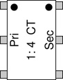
Transformers |
|
Transformers come in many shapes and sizes. The symbol given here works well for the commonly encountered centre tapped audio transformers most likely to be found in DIY audio circuits. The primary winding is to the left, with the secondary to the right. Both windings are centre tapped (the middle connections on either side), with the dots indicating the connections to the start of each winding. Differentiating start and end is important in maintaining the desired polarity in the signals passing through the transformer. The labelling here indicates the turns ratio (1 : 4) and that the transformer provides centre taps (CT). |
Diodes |
|
The diode symbol unsurprisingly sports a stripe on one end, matching the common markings on a real diode. In common with the polar capacitor described above, diodes must be inserted into a circuit in the correct orientation. The third symbol, representing an upright component, is similar to the equivalent resistor symbol. It is important to interpret this symbol with a little more care however, as orientation matters. The circle in this case is coloured in dark. This is intended to suggest that the end with the dark stripe is uppermost, and therefore should be connected to the point offset from the centre, with the non-striped end falling directly below the body of the symbol. The second set of three symbols here represent LEDs. Again orientation is important, and the flattened off side where one of the two leads originates indicates the LED’s negative lead (equivalent to the stripe in the standard LED). |
Transistors |
The two sets of outlines here actually represent the two most commonly encountered three pin semiconductor packages. Most transistors will come in one of these two forms but other semiconductor devices can also be encountered packaged in these standard packages. There are three pins and it is always important to get them the correct way around. The first package type is called TO-92 and the second is designated TO-220. In the case of TO-92 orientation is easy to specify by indicating in which direction the flat face should point. For the TO-220 package it is not so straightforward. The thick line on one side of the symbol is used here to indicate the back of the device. TO-220s are relatively high power dissipation devices, designed to have heat sinks attached. The thick line indicates the face to which a heat sink is attached. |
|
DIP ICs |
|
DIP IC stands for dual-in-line package integrated circuit. The dual-in-line bit means there are two parallel lines of legs, positioned on either side of the device’s body. The semicircle at the top allows the device to be placed the correct way around, which is of course essential. Some DIP ICs have a dot at pin one instead of, or as well as, the semicircle (pin one is at the top left in this picture, and pins are numbered counterclockwise from pin one, down the left side and back up the right). |
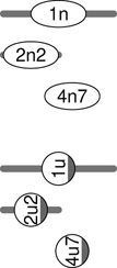
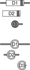

As a very basic example, consider the circuit shown in Figure 7.11. It consists of two components, a resistor and an LED in series, connected between +9V and 0V. There are many possible layouts which would work for such a simple circuit. Figure 7.12 shown a couple of possibilities. It also illustrates a few of the commonest errors made by inexperienced breadboard builders. Notice also how the 0V and +9V connections are distributed to the busses on both sides of the board. This is not really necessary for simple circuits, but it is a common practice where more elaborate layouts are concerned (see for instance Figure 11.9 (p. 177)). As mentioned earlier, the noise gate example at the end of this chapter does not follow this procedure, as one of the busses is actually used for other connections.

Figure 7.11 a simple circuit.
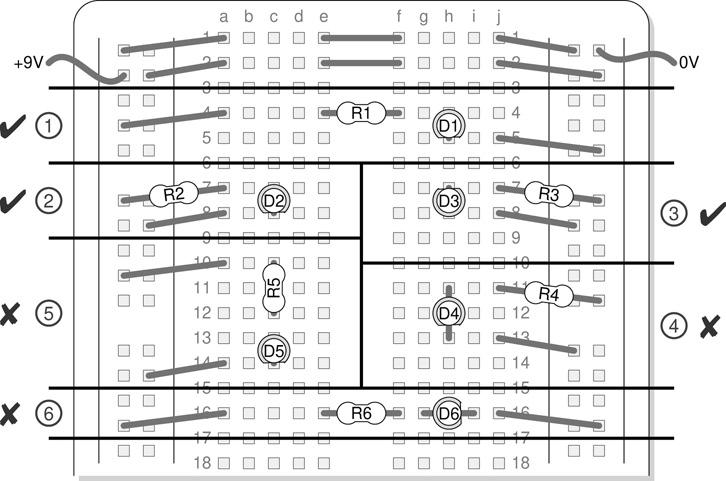
Figure 7.12 Some correct and incorrect layouts of the circuit shown in Figure 7.11.
Figure 7.12 shows six different attempts to layout the circuit, numbered (1) through to (6). Numbers (1) to (3) are all valid layouts, although it should be noted that (3) reverses the order of the resistor and LED. This makes no difference in this very straightforward circuit. It is often the case that two simple components in series with nothing else connected where they join can be reversed without ill effect. Notice that in the noise gate schematic in Figure 7.16, SW1 comes before R13 on the way down to ground. However in both the breadboard and the stripboard layouts which follow the order has been reversed to allow for a simpler layout design.
Layouts (4), (5), and (6) illustrate different layout errors. In (4) the diode is connected the wrong way round. Care must be taken to make sure that directional components such as diodes and polar capacitors are oriented correctly. Numbers (5) and (6) illustrate two related issues which arise from the visually tidy results of placing components in a line. Inserting two components in line vertically as in (5) does not result in a connection between them, they must be inserted on the same row. Similarly, it is almost never going to be correct to insert more than one of a component’s legs into the same row of five, as is done in (6). In this case it short-circuits the legs of the diode, bypassing it and effectively removing it from the circuit.
Layout Drafting Options
It is quite a simple matter to hand draft breadboard (and stripboard) layouts using squared paper but a software option is usually going to be easier. There are many software packages available which will do the job but a good free solution is a program called DIYLC (‘Do-It-Yourself Layout Creator’). Freely downloadable versions are available for PC and Mac. Note that this is just a drawing package, it does not run circuit simulations as some more elaborate software does. Chapter 8 mentions a few of the more accessible options in this department.
Stripboard Layouts
Once a project has been successfully breadboarded, and a final version has been settled on, the next step is to develop a stripboard layout for soldering up into a permanent circuit. (Various alternatives are discussed in Chapter 10 but stripboard is the medium used throughout this book.) Stripboard consists of a rigid circuit board material with a matrix of holes drilled in it, and parallel copper traces running across the board connecting together each row of holes. Figure 7.13 shows two images of the same piece of stripboard, viewed from either side.
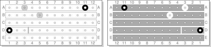
Figure 7.13 A piece of stripboard, showing views of the component and copper clad sides of the board side by side. Note that column numbering is mirrored left to right between the two views.
On the left is the component side, and to its right the copper side. Components are inserted on the component side with their legs sticking through the holes to emerge on the copper side, where they are soldered into place. While most of the layout work is done on the component side, it is useful to maintain a view from the copper side in tandem because breaks in the copper strips are almost always needed in order to complete a design, and these must be correctly located on the copper side. As the board is turned over and back it is very easy to get mixed up as to what is where. If the board is turned over like the page of a book, perspective changes from the left hand view to the right, as illustrated. Notice that the numbers 1–12 along the top and bottom boarders of the board are mirrored in the copper side view on the right, running 12–1.
Three types of feature have been indicated on this figure, and their locations match between the two views. The black ring along the left boarder at 1D is mirrored over to the right in the second view but is still at position 1D, and likewise for each of the other features indicated. Black rings indicate mounting holes drilled through the board. Light rings indicate breaks in the copper strip located over holes, and light bars indicate breaks cut into the copper between holes. The former are easier to work with but they do use up a hole, while the latter don’t require to use a hole but can be quite tricky to apply, and are easily overwhelmed by solder during the building process. The on-hole breaks can be made using a drill bit or a dedicated little hand tool called a spot face cutter. It is important to check that the hole is cut deep enough to complete the break. It is easy to leave a tiny sliver of copper connecting across the intended break point. A craft knife or other sharp point can be used to scrape a between-hole break into the copper strip. The layouts presented here generally stick to on-hole breaks for simplicity’s sake.
Figure 7.14 shown an alternative arrangement with the copper side located below instead of beside the component side. Notice that this time it is the letters along the rows which are flipped, rather than the column numbers as before, but once again the breaks and holes retain the correct indices between the two views. This time only the drilled holes are actually placed on both views. The component side can quickly get cluttered, and it is better to leave the breaks out in this view. Using the indices it is a simple matter to check that they are in the correct locations, even on a large layout. In this case notice for instance that the column of four breaks from 7A to 7D run under the DIP IC labelled TL072. This is a common thing to see, as the two sets of pins on a DIP must be isolated from each other.

Figure 7.14 Stripboard with the copper side view placed below the component side view. Here the row letters are flipped top to bottom, rather than the column numbering left to right as in Figure 7.13.
Two other features are illustrated on this board: jumper wires and fly leads. Jumper wires connect two points on the board. They are most often run vertically but can be routed at an angle if need be. As illustrated, they can (with care) be run underneath a DIP. An outline is used here to show such a routing. In addition, a connection between two immediately adjacent points (as in 8B to 8C here) can be achieved simply by applying sufficient solder so as to bridge the gap. As such the connection here can be overlayed on other connections, in this case two pins of the IC. While these two options can be convenient in tight layouts, they have been avoided in the projects presented in this book in order to maintain maximum clarity.
Fly leads are wires coming off the board to other components, usually such things as battery clips, connector jacks, switches, and pots. The convention adopted here is simply to label all such connections, rather than using graphical symbols for the components in question. This leads to tidier layouts as it avoids the necessity to bring together the various leads connecting to any given off-board component. Careful labelling ensures that all such connection points are unambiguously connected to the correct terminals on each of these offboard components. Note that these jump lead and fly lead connections, and all the notes associated with them here, apply equally to breadboard layouts, where they can be used in exactly the same fashion, with the exception that the two routing options (under components and shared connection points) do not apply to breadboards.
A More Elaborate Example
To round out this chapter an ambitious circuit layout task will be examined. The circuit in question implements a noise gate. Much audio electronic circuitry can be quite noisy, some electric guitar effects pedals are particularly bad offenders. A noise gate is often added to the end of such a noisy signal chain in order to keep the noise level down when the instrument is not being played. When the signal level coming into the noise gate drops below a certain threshold, the gate closes and the noise is prevented from emerging at the output of the signal chain. The idea is that the threshold is set just above the noise floor so that when the guitar is played the threshold is breached and the gate opens. Obviously a gate can only be effective when the threshold can be adjusted to a band between the level of the noise floor and the quietest signal level which is needed to open the gate.
The circuit here provides two controls. A threshold control is of course needed so that the gate can be configured for the particular levels of signal and noise present. An override switch is also implemented. Usually as the guitar sound dies away below the set threshold, the gate will close. Sometimes a player wants the long decay to be preserved. In this case the override switch is kept pressed as the sound dies away, for as long as the decay is desired. On release the gate will close, preventing further low level signal from passing. A block diagram of the system is given in Figure 7.15, showing signal flow, functional blocks, and user controls, but no implementation details. This is the level of information the user needs in order to get the most out of the device. To build the circuit, a little more concrete detail is required.

Figure 7.15 Noise gate circuit block diagram.
Figure 7.16 shows the complete circuit diagram for the noise gate. As described earlier, such things as powering options and bypass circuitry are omitted. In fact these will not be included in the layouts here either, as they would be implemented as off-board connections in the final build. Here only the circuit board layouts are considered (the complete procedure to build a working project is addressed in Chapter 10). This is a particularly tricky circuit to address for a number of reasons. It is quite large for the class of project being considered (although not the largest), but in addition it entails some quite complex connectivity.
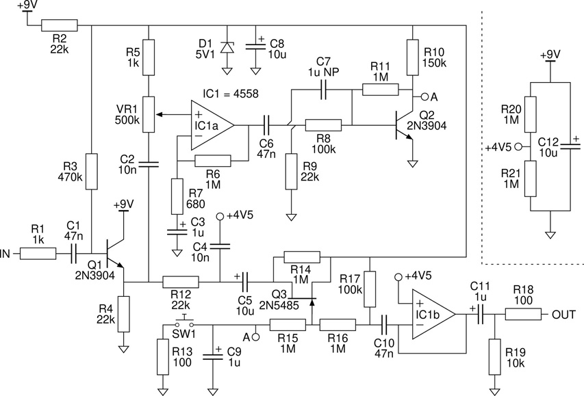
Figure 7.16 Noise gate circuit schematic.
The two opamps, IC1a and IC1b, are implemented through a dual opamp IC. Using two single opamp chips is perfectly valid, and variants of this circuit exist which do exactly that. Since the aim here is to tackle the challenge rather than to avoid it, this simplifying design choice has not been embraced. Another complex routing challenge encountered here starts at R2 in the schematic in Figure 7.16 and snakes around the circuit connecting together a total of nine disparate components. Another six way connection point hangs from the collector of Q2. The ground buss is traditionally the busiest connection point and in this case a total of 15 nodes come together here. Routing multiple multi-way connections neatly can prove a difficult task.
Figure 7.17 illustrates a possible breadboard layout for the noise gate circuit. As noted, this circuit presents a number of challenges when it comes to developing a viable layout. As such it represents a good example to examine. It is important to note that there is no step by step formula which will reliably result in a breadboard layout. A certain amount of trial and error is inevitably involved. There are two useful approaches to getting a layout started; either start from the input and work through the signal flow, or start with the most interconnected component (in this case IC1) and work out.
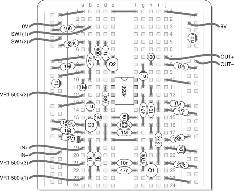
Figure 7.17 Breadboard layout for the noise gate circuit.
When attempting a difficult layout false starts are inevitable and can be useful in clarifying where the difficulties lie. It can be most productive to abandon a layout which has hit a blockage, and start again using what has been learned to improve the chances of a successful conclusion next time around. When laying out this circuit, I started my first attempt working out from IC1 but couldn’t arrive at a layout I was happy with. It started to get very messy. This attempt was scrapped, and I tried again starting this time at the input. The second attempt lead to the layout presented here. Having identified the two most complex connection points in the first pass (the nine and six way connection points mentioned above), I highlighted these on my circuit diagram, and kept an eye on how they might layout as I worked.
Given the number and distribution of ground connections (15 in all), it was clear that a vertical buss on each side of the board dedicated to these would be required (the three jumper wires across the top of the board make this connection), but since there were fewer +9V connections (six in total) it was decided to try to keep these to one buss and reserve the fourth and final buss for other purposes. With the power connection to IC1 on the right it made sense to reserve the buss on this side, and leave the second left hand side buss free. This ended up being used for the six way connection point hanging off the collector of Q2. The nine way connection point occupies four rows around the board. Three jumper wires can be seen linking these up: d16–d18, e18–f18, and h18–h19. Identifying these key points in the circuit makes it easier to follow the various connections and confirm the accuracy of the layout.
Having built and tested the breadboard version, and decided that a permanent version is wanted, the next task is to arrive at an equivalent stripboard layout. It is possible to convert a breadboard layout almost directly into a stripboard version (the busses present difficulties but these are not insurmountable). However such a layout will not result in terribly efficient use of space on the stripboard, and is likely to be somewhat inelegant. Better to start from scratch. Figure 7.18 illustrates a possible stripboard layout for this circuit. Stripboard layouts tend to entail components almost exclusively being laid out vertically. Breadboards tend to result in much more of a mix, as connections to the busses and across the central gap lay out horizontally, while the rest tend to run vertically. It is by no means a requirement that fly leads exit the board from around the edge, but aiming for this does make a tidier layout, and also results in a slightly easier layout to build. The final project in Chapter 11 has a stripboard layout (see Figure 11.15, p. 185) where a compact layout has been favoured over following this general rule. Some might say this layout is rather too compact. It certainly does make for a challenge to solder it all up in such a small footprint. At this level, it is simply a question of personal preference.

Figure 7.18 Stripboard layout for the noise gate circuit.
As already stated, these layouts represent quite a difficult and challenging layout design task. Once a bit of practice and experience has been gained laying out smaller and more straightforward circuits, the reader might consider the challenge of returning to this project and attempting to complete a breadboard and a stripboard layout of their own. It might take a few attempts before a satisfactory result is achieved. It is unlikely to look too much like the examples given here. There are many possible layouts, and most certainly layouts which complete the task more elegantly or simply.
References
C. Coombs. Printed Circuits Handbook. McGraw-Hill, 6th edition, 2008.
Elektor. Tup-tun-dug-dus. Elektor, 1(1):9–11, 1974.
A. Sedra and K. Smith. Microelectronic Circuits. Oxford University Press, 7th edition, 2014.
E. Young. Dictionary of Electronics. Penguin, 1985.