18 | Integrated Circuits
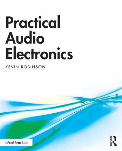
Integrated circuits (ICs) are just circuits pre-wired on a silicon chip. They can come in a lot of shapes and sizes, but the ones used here are almost all in DIL (dual in-line) packages, Figure 18.1b. The name refers to the fact that there are two rows of legs for making connections. This is a through hole format; the legs are designed to be inserted through holes on the circuit board and be soldered on the other side, as opposed to surface mount packages which are also common, but which are not discussed here. Related commonly seen abbreviations for the same package style are of the form DIP8 and DIP14. The DIP stands for dual in-line package, and the number refers to the number of legs, so for instance the 386 power amplifier chip encountered a few times already would be described as coming in a DIP8 format. An obvious variation on this theme is the SIL or single in-line package. An example of this style is the three pin LM317 voltage regulator, which is introduced later. Obviously most transistors could also be referred to as being SIL packages. SIL packages with a leg count over three are less common but by no means unheard of.
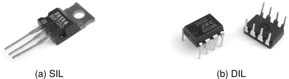
Figure 18.1 Typical integrated circuits in (a) SIL and (b) DIL packages.
When using ICs remember that it is almost always necessary to provide power to the chip, even if these connections are not shown in the circuit diagram for the circuit being built. If not all elements on a chip are being used in the circuit, it is often a good idea to tie unused inputs either to ground or sometimes to the positive voltage rail or some other available reference voltage, in order to minimise noise and interference. See also Chapter 7 for some additional notes on this topic.
Selected ICs
Table 18.1 lists some commonly encountered ICs. Some of these are examined in more detail in the sections which follow. All are worth getting familiar with. As usual a good place to start is with the manufacturer’s data sheets for the devices. A quick search online will yield the relevant documents (and can quickly lead down the rabbit hole of online forum discussion threads and similar valuable, though sometimes variable quality, resources).
Category |
Example part # |
Notes |
Opamp (single) |
LM741 |
Very common (though now very old) opamp |
“ |
LF356 |
JFET inputs gives high Zin |
“ |
NE5534 |
Low noise opamp |
Opamp (dual) |
TL072 |
Popular dual opamp with JFET inputs |
“ |
LM358 |
Works well close to power rails |
“ |
NE5532 |
Dual version of the NE5534 low noise opamp |
Opamp (quad) |
LM324 |
Four opamps in a single fourteen pin package |
OTA |
NJM13700 |
One of very few OTAs still available |
Power amp |
LM386 |
Common, easy to use low power audio amplifier |
“ |
LM380 |
For a little more power than the 386 can provide |
Voltage regulator |
LM317 |
Output voltage adjustable from 1.25V to 37V |
“ |
LM337 |
Negative power rail equivalent of the LM317 |
Precision timer |
NE555 |
Popular timer chip, found in many audio projects |
“ |
NE556 |
Two 555 timers on one chip |
Digital delay/echo |
PT2399 |
Single chip digital delay/echo processor |
Tone decoder |
LM567 |
Re-purposed by DIYers to make interesting noises |
4000 series |
various |
See Table 18.4 for some examples |
Optocoupler |
NSL-32 |
LED/LDR optocoupler |
Opamps
The operational amplifier (opamp) is the most important and most commonly encountered standard circuit building block in audio electronics, and as such a significant portion of this chapter is dedicated to understanding and using opamps effectively. Opamps come in two forms, either prefabricated as ICs, or built from the ground up from discrete components. IC opamps make life a great deal easier for the audio circuit builder, and here only the IC approach to opamp circuit construction is considered. Opamps are one of the most fundamental building blocks of audio circuits, so it is important to have a good grasp of how they are used.
The practical operation of an opamp is very straightforward; the output is just a greatly amplified version of the difference between the two inputs. This relationship is expressed in Eq. 18.1. The triangle symbol in Figure 18.2 is the standard representation in electronic circuit diagrams for an amplifier in general and for an opamp in particular. In this case the G inside the triangle represents the opamp’s open-loop gain. The only important thing to remember about this is that it is a very big number. So, by Eq. 18.1, Vout is equal to the difference between the two inputs multiplied by a very big number. This rule never changes and is key to understanding how opamp circuits work.
The other important rule to remember about opamps is that the inputs generally have very high input impedances. This means that their effect can usually be ignored when analysing how a circuit is going to behave. These two rules, very high gain and very high input impedance, are all the knowledge about opamps that is really needed to analyse basic opamp configurations.
Negative Feedback
In fact this open loop gain G is far too high to be used directly as the amplification factor in most analog circuits; even the tiniest input signal would appear at the output too large to be useful. A simple trick allows this gain to be brought under control, and set and varied exactly as required in a typical amplifier application. That simple trick is called negative feedback (NFB). Most opamp circuits which will be encountered employ negative feedback in order to achieve signal control. The thing to look for in order to identify the application of negative feedback is a pathway (usually involving a resistor) from the opamp’s output back around to its negative (or inverting) input (Figure 18.3). The inverting input is usually labelled with a minus sign, with the noninverting input labelled with a plus, as illustrated in the Figure 18.2.

Figure 18.3 Negative feedback from output to inverting input.
Negative feedback allows the excessive open-loop gain G to be turned into a smaller (and controllable) closed-loop gain, represented as g. So the transfer function for an opamp circuit employing negative feedback is as in Eq. 18.2. (Recall that a transfer function is simply an equation defining the output in terms of the input.) So the output is just the input multiplied by this new lower gain factor, g, as expected.
Negative feed back leads to a simple rule for analysing the behaviour of any opamp circuit which uses it:
To understand why this is so, consider what happens if either input is moved away from the other in either the positive or the negative direction. Always remember that the fundamental, unchangeable behaviour of an opamp is described in Eq. 18.1.
Referring to the inputs as V+ for the noninverting input and V− for the inverting input, and the output as Vout, if V+ moves a bit above V−, then Vout wants to move up a lot (by Eq. 18.1). However, as Vout starts to move up, its negative feedback connection to V− pulls V− up along with it. This brings V− back level with V+ again, and so Vout no longer wants to move, since what it amplifies is the difference between V+ and V−.
Exactly the same thing happens if V+ moves below V−. This time Vout moves down, again pulling V− with it, and again both settle at a new equilibrium. And so the negative feedback combined with the very large open-loop gain G prevents the two inputs from diverging. If they try, the negative feedback pulls them back together.
It is then a question of how to set the value for the closed-loop gain, g, and the operation of the negative feedback opamp circuit is known. The setting of g is down to the configuration of the circuit involved. Two standard circuit configurations are examined below. They are called the inverting and the noninverting configurations. The names indicate which of the opamp’s two inputs has the input signal connected to it, and as a result, whether or not the output signal is inverted relative to the input.
Inverting Configuration
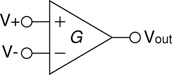
Figure 18.4 illustrates the standard inverting configuration for an opamp. The noninverting pin (+) is tied to ground, and the input signal is applied to R2, which feeds into the inverting input (−). R1 implements the negative feedback. The gain which this configuration achieves is defined by Eq. 18.3. The gain factor is simply the ratio of the resistors used. The minus sign in Eq. 18.3 indicates that this circuit will invert the polarity of the input signal when it appears at the output.
Figure 18.4 Opamp inverting configuration.
It thus becomes a simple matter to design a circuit which will (for instance) double the size of a signal. (The signal will also always be inverted using this circuit. The next section presents the noninverting option.) If the gain is to be −2, then by Eq. 18.3 R1/R2 must equal 2, and so R1 must be twice the size of R2. Clearly many pairs of values satisfy this requirement. One value must be chosen and then the second can be calculated. There are tradeoffs favouring smaller and larger resistor values in such circuits, but values around the 10k to 100k range are often a reasonable place to start. So if R1 = 50k were chosen, then the second value would be calculated as R2 = R1/2 = 25k.
The behaviour of this circuit is illustrated on the right in Figure 18.4, where the lengths of the lines are proportional to the resistor values R1 and R2. The lines start at Vin and end at Vout, with the crossover point locked in at zero volts where R1 and R2 meet. In this case R1 is twice the size of R2, and so the end of the line at Vout moves twice as far as that at Vin. Changing the relative lengths of R1 and R2 changes the relationship between Vin and Vout, precisely as specified in Eq. 18.3. Notice that this is the inverting configuration so that when Vin goes up Vout goes down, and vice versa.
Noninverting Configuration
Figure 18.5 shows the noninverting opamp configuration. In this case R2 is tied to ground, and the input signal Vin is applied to the noninverting opamp input (+). As always, the golden rule of negative feedback applies, and the minus and plus inputs stay locked together. This is illustrated on the right of Figure 18.5 where the point between R1 and R2 (connected to minus) is shown to track Vin, which is the signal at plus.
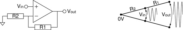
Figure 18.5 Opamp noninverting configuration.
The analysis of the noninverting configuration proceeds along the same lines as the inverting case. The voltage at the minus input tracks Vin due the negative feedback provided by R1. This time Vin and Vout always move in the same direction, with the far end of R2 tied to 0V. Thus the result is a non-inverted output.
Notice that if R1 becomes zero (a short circuit), then the gain equals one. In fact, the configuration shown in Figure 18.6 can be seen as a special case of the general noninverting opamp configuration where R1 = 0 and R2 = ∞ (i.e. a short circuit and an open circuit respectively). This arrangement is very commonly encountered, and is referred to as a voltage follower or unity gain buffer. With a gain of one, output simply equals input at all times (Eq. 18.5).

Figure 18.6 Opamp voltage follower (unity gain buffer) configuration.
The voltage follower is often encountered inserted between sections of a circuit. It would appear on first analysis to play no role in the operation of the wider circuit, as the output simply equals the input. What it does is to buffer one part of a circuit from another, while still passing signal from one side to the other. This isolation can be very useful, preventing unwanted interactions between the sides.
Single, Dual, and Quad Opamp Packages
Opamps come in a number of standard IC packages, containing one, two, or four opamp circuits on a single chip. While it is always good practice to check the pinout for a particular device, the arrangements shown in Figure 18.7 are unlikely to be deviated from. One consequence of these standardised footprints is that it facilitates drop-in replacements. While not always the case, it is often possible to swap one device for another of the same configuration. This can be done in order to achieve lower noise or better linearity for instance. A TL072 might be replaced by an NE5532 for example. These are both dual opamps (see Table 18.1), and thus share a common pinout.
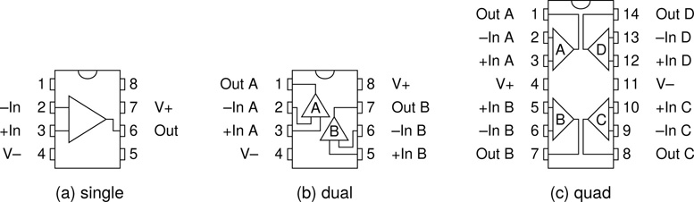
Figure 18.7 Standard pinouts for single, dual, and quad opamp ICs.
Some circuits rely on specific characteristics of the opamps they use, which may not be shared by potential replacement parts, so this procedure will not always work, but it is a common practice in many circuits, where better (or just different) performance is sought.
The unlabelled pins on the single opamp pinout (1, 5, and 8) are used in different ways on different devices, but are often left unconnected, and so drop-in replacements may still work, but it is a good idea to examine these pins in order to spot potential pitfalls before attempting a swap.
IC Power Amps
Many IC power amps exist, but the most commonly encountered for low power audio work has got to be the 386. Others are well worth investigating if a little more power is required. The range of 386 chips available top out at about 11/2W, and distortion levels are getting pretty high by then. As a simple lo-fi utility amp however, the 386 is hard to beat. As such it is the device considered here, and the one used in numerous other places throughout this book.
LM386/JRC386 Low-Power Audio Amplifier
The 386 low-power audio amplifier Ic can be encountered in a number of places throughout this book. It is a workhorse of audio electronics builders and very many circuits have been designed around this chip. Several have already been encountered and Figure 18.8 adds to the possibilities, presenting two of the simplest possible power amp circuits. The bare-bones amp in (a) provides a signal gain of 20, which can be plenty in many situations, but for a bit more amplification (b) adds a gain switch between pins 1 and 8. When the switch is closed, the gain jumps from 20 to 200. The capacitor on pin 7 helps stabilise the amp at higher gains.
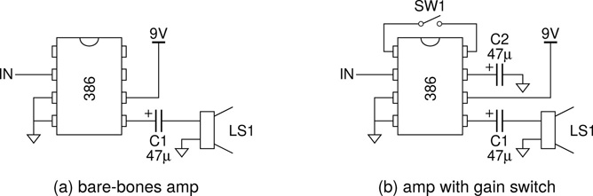
Figure 18.8 Two very simple 386 based amplifier circuits.
LM317 Voltage Regulator
Using a voltage regulator provides a number of advantages over an unregulated power supply. Voltage regulators can eliminate noise, and provide output voltages which are both precise and stable, even with a poorly defined, noisy input voltage prone to drift. There are many options available, both fixed and programmable. Fixed variants are simple to use but provide only one possible regulated output voltage.
Here the LM317 programmable voltage regulator is considered. For good regulation the input voltage needs to be at least 3V above the output. In other word, if a 9V input is used, a regulated output up to 6V can be reliably generated. (The minimum output level is 1.25V, regardless of input.) The input voltage can be as high as 40V, which means regulated outputs between 1.25V and 37V are possible. The output current can be as high as 1.5A, but this kind of level will certainly require a heat sink. Lighter loads may not require heat sinking – if the power dissipated by the regulator ((Vin−Vout)×Iout) does not exceed 1/4W then no heat sink is required.
Figure 18.9 shows the basic configuration used to set the output voltage of an LM317. R1 is typically kept between about 120Ω and 1k2Ω, with 240Ω being a commonly used value. Once R1 has been selected, R2 can be calculated using the expression shown in Eq. 18.6.
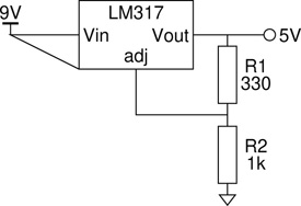
Figure 18.9 How to configure an LM317 voltage regulator.
Since usually only a limited number of resistor values will be available, it can take a bit of work to find a pair of available values which give a result close enough to the target level. The values shown here in Figure 18.9 (R1 = 330 and R2 = 1k) are very commonly available resistor values, and give a result very close to 5V. If a very particular output voltage is needed, R2 can be replaced with a trim pot, or alternatively a regular pot can be used to provide a user variable output voltage level.
NE555 Precision Timer
The 555 timer has long been a favourite with audio circuit builders. This chip can be used to make simple and versatile oscillator circuits. In Figure 18.10 the pinout for the 55 can be seen, alongside its big brother, the 556. This second chip is just two 555 timer circuits packaged up into one IC.

Figure 18.10 Pinouts for the 555 timer and the 556 dual timer.
A wide range of circuits can be found in Mims (1996) including the stepped-tone generator, a variation of which can be seen in Figure 18.11. This circuit is examined in detail in one of the projects presented in Chapter 11.
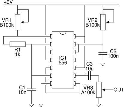
Figure 18.11 The stepped-tone generator circuit from Chapter 11 is a very popular 555 based circuit. Here it is built using a 556, but two 555s can also be used.
4000 Series ICs
The 4000 series consists of a large collection of utility ICs, mainly intended for building digital logic control oriented circuitry. Many have been pressed into service in audio circuits, in various imaginative ways. Often the first to be encountered in this context is the CD40106 hex Schmitt trigger inverter, which with the addition of only a resistor and a capacitor, can be used to build an oscillator (six oscillators potentially, since the ‘hex’ in the name indicates that the IC contains six inverters). The practical exercise below explores a similar circuit which uses NAND gates (courtesy of the CD4093) rather than inverters. An excellent source of ideas for 4000 series circuits is Collins (2009).
Table 18.4 lists a small selection of 4000 series ICs which can be particularly useful in making interesting audio circuits. A brief note on some potential uses for each are provided below, but the possibilities are endless.
Part |
Package |
Description |
CD4040B |
DIP16 |
12 bit binary counter |
CD4051B |
DIP16 |
single 8 channel multiplexer |
CD4053B |
DIP16 |
triple 2 channel multiplexer |
CD4066B |
DIP14 |
quad bilateral (spst) switch |
CD4069UB |
DIP14 |
hex inverter (unbuffered) |
CD4070B |
DIP14 |
quad 2 input XOR (exclusive OR) |
CD4093B |
DIP14 |
quad Schmitt trigger 2 input NAND |
CD40106B |
DIP14 |
hex Schmitt trigger inverter |
The CD4040 is a 12 bit binary counter. Each time the counter’s input goes from high to low, the 12 bit binary count goes up by one. This doesn’t sound much use until you realise that a 12 bit binary number counting up looks like twelve square wave, each with a frequency half that of the one before. So putting an LFO into the input generates twelve synchronised square waves on the twelve outputs. These can be used directly as audio signals, or they can be used as control signals. They are often used in this second way, fed into the control inputs of the 4051 multiplexer (see below).
The CD4051 is a single 8 channel multiplexer. This is basically a digitally controlled single pole eight throw (sp8t) switch. Three binary digits let you count to eight, so three digital inputs control the switch, selecting which throw is currently connected. Pick three of the twelve square waves coming out of the 4040 above, and you get a nice repeating switching pattern jumping around the multiplexer channels.
The CD4053 is a triple 2 channel multiplexer, three independent spdt switches, controlled by digital inputs. Where a standard spdt switch appears in a circuit, this chip might be used to replace it with an electronic switch, perhaps controlled from an arduino or similar microcontroller, or depending on what the switch does, driven from a simple square wave oscillator.
The CD4066 is a quad bilateral (spst) switch. This one has been widely used for implementing electronically controlled bypass switching on effects circuits, but again, wherever an spst switch is called for one of these might be considered for some automated control.
The CD4069 is an unbuffered hex inverter which can be found used in booster and distortion circuits. As with many of the applications suggested here, this is somewhat outside the intended application of this device. Several interesting applications can be found in the ‘Circuit Snippets’ collection which has been referenced several time throughout this book.
The CD4070 is a quad two input XOR (exclusive OR). This gives a high output if and only if one input is high and the other is low; if both are low or both are high, the output is low. This chip is used to good effect to build a ‘digital ring modulator’ in Penfold (1986).
The CD4093 is a quad Schmitt trigger two input NAND. This is the chip used here in Learning by Doing 18.3 to build a couple of cascaded oscillators. The Schmitt trigger bit of the name means that the switching of these gates does not happen symmetrically about the mid voltage level. Instead, inputs moving low to high need to go higher, and inputs moving high to low need to go lower, before switching happens. This is a common situation, used to eliminate unwanted switching with noisy inputs. This same property makes these Schmitt trigger variants (both this and the 40106 below) better options than non-Schmitt trigger types for building oscillators.
The CD40106 is a hex Schmitt trigger inverter. Inverters are also called NOT gates; the output is NOT the input, i.e. it is inverted. The 40106 is very commonly encountered used to build simple oscillators. This is done in the same basic way as with the 4093, used in the exercise below, needing only a resistor and a capacitor in order to make a working oscillator.
Analog Optocouplers
Optocouplers (aka opto-isolators) come in a number of different forms, but usually involve an LED shining on a light sensitive device of some kind. In the two symbols illustrated in Figure 18.12 the sensors indicated are a photoresistor and a phototransistor respectively – other possibilities also exist. Optocouplers provide electrical isolation between their two sides; while this is their primary intended application, they can also add interesting distortion to an audio signal, as well as providing other novel control options.

Figure 18.12 Symbols for photoresistor and phototransistor based optocouplers.
The two names given above highlight these devices primary characteristics; ‘-coupler’ because they can pass a signal from one side to the other, ‘-isolator’ because they provide electrical isolation between the two sides while doing so, and of course the ‘opto-’ part indicates that the way all this is achieved is through the use of light.
A signal entering on one side of the device causes the LED within to shine brighter and dimmer, in time with the variations in the signal. This varying light level causes the detector element on the other side (photoresistor, phototransistor, or whatever) to adjust its output in time with the varying light. Much of the distortion which is introduced (most especially in the photoresistor variety) is due to the slow response such devices have to changes in light level. It takes a little time for the resistance of a photoresistor to change in response to the changing intensity of the light falling upon it. This can for instance result in a satisfying softness in the response of compressors and limiters built using these devices.
Commercial optocouplers most often combine an LED with a phototransistor, and this configuration certainly merits experimentation also, but the easiest approach to a homemade optocoupler uses a photoresistor (or LDR) as the detector. This is the approach used in the exercise below.
References
G. Clayton and S. Winder. Operational Amplifiers. Newnes, 5th edition, 2003.
N. Collins. Handmade Electronic Music. Routledge, 2nd edition, 2009.
W. Jung, editor. Op Amp Applications Handbook. Newnes, 2005.
F. Mims. Engineer’s Mini-Notebook: 555 Timer IC Circuits. Radio Shack, 3rd edition, 1996.
R. Penfold. More Advanced Electronic Music Projects. Bernard Babani, 1986.
R. Severns, editor. MOSPOWER Applications Handbook. Siliconix Incorporated, 1984.
TI. The TTL Data Book. Texas Instruments, 5th edition, 1982.
R. Widlar et al. Linear Applications Handbook. National Semiconductor, 1994.