
Project 17 – Shift Register 8-Bit Binary Counter
In this project, you're going to use additional ICs (Integrated Circuits) in the form of shift registers in order to drive LEDs to count in binary (I will explain what binary is soon). Specifically, you will drive eight LEDs independently using just three output pins from the Arduino.
Parts Required
| 1 × 74HC595 Shift Register IC | |
| 8 × 220Ω Resistors* | |
| 8 × 5mm LEDs |
Connect It Up
Examine the diagram carefully. Connect the 3.3V to the top rail of your breadboard and the Ground to the bottom. The chip has a small dimple on one end; this dimple goes to the left. Pin 1 is below the dimple, Pin 8 is at bottom right, Pin 9 is at top right, and Pin 16 is at top left.
You now need wires to go from the 3.3V supply to Pins 10 and 16, and wires from Ground to Digital Pins 8 and 13. A wire goes from Digital Pin 8 to Pin 12 on the IC. Another one goes from Digital Pin 12 to Pin 14 on the IC and finally one from Digital Pin 11 to Pin 11 on the IC.
The eight LEDs have a 220 ohm resistor between the cathode and ground, then the anode of LED 1 goes to Pin 15. The anode of LEDs 2 through 8 goes to Pins 1 to 7 on the IC.
Once you have connected everything, check again that your wiring is correct and that the IC and LEDs are the right way around.
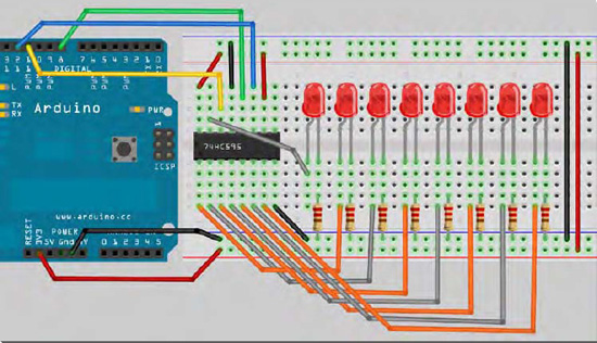
Figure 6-1. The circuit for Project 17 – Shift Register 8-Bit Binary Counter (see insert for color version)
Enter The Code
Enter the following code in Listing 6-1 and upload it to your Arduino. Once the code is run, you will see the LEDs turn on and off individually as they count up in binary every second from 0 to 255, then start again.
Listing 6-1. Code for Project 17
// Project 17


int latchPin = 8; //Pin connected to Pin 12 of 74HC595 (Latch)
int clockPin = 12; //Pin connected to Pin 11 of 74HC595 (Clock)

int dataPin = 11; //Pin connected to Pin 14 of 74HC595 (Data)
void setup() {

        //set pins to output

        pinMode(latchPin, OUTPUT);

        pinMode(clockPin, OUTPUT);

        pinMode(dataPin, OUTPUT);

}


void loop() {

        //count from 0 to 255

        for (int i = 0; i < 256; i++) {

                //set latchPin low to allow data flow

                digitalWrite(latchPin, LOW);

                shiftOut(i);

                //set latchPin to high to lock and send data

                digitalWrite(latchPin, HIGH);

                delay(1000);

        }

}


void shiftOut(byte dataOut) {

        // Shift out 8 bits LSB first, on rising edge of clock

        boolean pinState;

        digitalWrite(dataPin, LOW); //clear shift register ready for sending data

        digitalWrite(clockPin, LOW);


        for (int i=0; i<=7; i++)  { // for each bit in dataOut send out a bit

                digitalWrite(clockPin, LOW); //set clockPin to LOW prior to sending bit


                // if the value of DataOut and (logical AND) a bitmask

                // are true, set pinState to 1 (HIGH)

                if ( dataOut & (1<<i) ) {

                        pinState = HIGH;

                }

                else {

                        pinState = LOW;

                }


                //sets dataPin to HIGH or LOW depending on pinState

                digitalWrite(dataPin, pinState); //send bit out on rising edge of clock

                digitalWrite(clockPin, HIGH);

        }

        digitalWrite(clockPin, LOW); //stop shifting out data

}
The Binary Number System
Before I dissect the code and the hardware for Project 17, let's look at the binary number system. It's essential to understand binary to be able to successfully program a microcontroller.
Human beings use a Base 10, or decimal number system, because we have 10 fingers on our hands. Computers do not have fingers, and so the best way for a computer to count is using its equivalent of fingers, which is a state of either ON or OFF (1 or 0). A logic device, such as a computer, can detect if a voltage is there (1) or if it is not (0) and so uses a binary, or base 2, number system as this number system can easily be represented in an electronic circuit with a high or low voltage state.
In our number system, base 10, we have 10 digits ranging from 0 to 9. When we count to the next digit after 9, the digit resets back to zero, but a 1 is incremented to the tens column to its left. Once the tens column reaches 9, incrementing this by 1 will reset it to zero, but add 1 to the hundreds column to its left, and so on:
000,001,002,003,004,005,006,007,008,009

010,011,012,013,014,015,016,017,018,019

020,021,023 ………
In the binary system, the exact same thing happens, except the highest digit is 1 so adding 1 to 1 results in the digit resetting to zero and 1 being added to the column to the left:
000, 001

010, 011

100, 101…
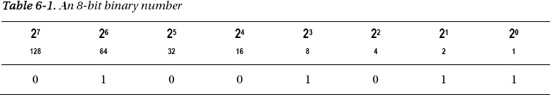
An 8 bit number (or a byte) is represented like in Table 6-1.
Table 6-1. An 8-bit binary number
| 27 128 |
26 64 |
25 32 |
24 16 |
23 8 |
22 4 |
21 2 |
20 1 |
| 0 | 1 | 0 | 0 | 1 | 0 | 1 | 1 |
The number above in Binary is 1001011, and in Decimal this is 75.
This is worked out like this:
1 × 1 = 1
1 × 2 = 2
1 × 8 = 8
1 × 64 = 64
Add that all together and you get 75. Table 6-2 shows some other examples.
…and so on.
![]() Tip You can use Google to convert between a decimal and a binary number and vice versa.
Tip You can use Google to convert between a decimal and a binary number and vice versa.
So to convert 171 decimal to binary, type 171 in binary into the Google search box which returns
171 = 0b10101011
The 0b prefix shows the number is a binary number and not a decimal number. So the answer is 10101011.
To convert a binary number to decimal, do the reverse. Enter 0b11001100 in decimal into the search box, and it returns 0b11001100 = 204
So now that you understand binary, let's take a look at the hardware before looking at the code.
Project 17 – Shift Register 8-Bit Binary Counter - Hardware Overview
You are using a shift register, specifically the 74HC595. This type of shift register is an 8-bit serial-in, serial or parallel-out shift register with output latches. This means that you can send data in to the shift register in series and send it out in parallel. In series means 1 bit at a time. Parallel means lots of bits (in this case 8) at a time.
Data is entered when the LATCH is set to LOW (this allows data to be sent to the chip) and sent out when the LATCH is set to HIGH. So you give the shift register data (in the form of 1's and 0's) one bit at a time, then send out 8 bits all at the exact same time. Each bit is shunted along as the next bit is entered. If a 9th bit is entered before the Latch is set to HIGH, then the first bit entered will be shunted off the end of the row and be lost forever.
Shift registers are usually used for serial-to-parallel data conversion. In this case, the data that is output is 1's and 0's (or 0V and 3.3V), so you can use it to turn on and off a bank of eight LEDs.
The Shift Register for this project requires only three inputs from the Arduino. The outputs of the Arduino and the inputs of the 595 are shown in Table 6-3.
| Arduino Pin | 595 Pin | Description |
| 8 | 12 | Storage Register Clock Input |
| 11 | 14 | Serial Data Input |
| 12 | 11 | Shift Register Clock Input |
Let's refer to Pin 12 as the Clock Pin, Pin 14 as the Data Pin, and Pin 11 as the Latch Pin.
Imagine the Latch as a gate that will allow data to escape from the 595. When the gate is lowered (LOW), the data in the 595 cannot get out, but data can be entered. When the gate is raised (HIGH), data can no longer be entered, but the data in the Shift register is released to the eight pins (QA-QH or Q0 to Q7, depending on your datasheet; see Figure 6-2). The Clock is simply a pulse of 0′s and 1′s, and the Data Pin is where you send data from the Arduino to the 595.

Figure 6-2. Pin diagram of a 595 chip
To use the shift register, the Latch Pin and Clock Pin must be set to LOW. The Latch Pin will remain at LOW until all 8 bits have been set. This allows data to be entered into the storage register (the storage register is simply a place inside the IC for storing a 1 or a 0). You then present either a HIGH or LOW signal at the Data Pin and then set the Clock Pin to HIGH. Setting the Clock Pin to HIGH stores the data presented at the Data Pin into the Storage Register. Once this is done, you set the Clock to LOW again, then present the next bit of data at the Data Pin. Once you have done this eight times, you have sent a full 8-bit number into the 595. The Latch Pin is now raised, which transfers the data from the storage register into the shift register and outputs it from Q0 to Q7 (Pin 15, 1 to 7).
This sequence of events is described in Table 6-4.
| Pin | State | Description |
| Latch | LOW | Latch lowered to allow data to be entered |
| Data | HIGH | First bit of data (1) |
| Clock | HIGH | Clock goes HIGH. Data stored. |
| Clock | LOW | Ready for next Bit. Prevent any new data. |
| Data | HIGH | 2nd bit of data (1) |
| Clock | HIGH | 2nd bit stored |
| … | … | … |
| Data | LOW | 8th bit of data (0) |
| Clock | HIGH | Store the data |
| Clock | LOW | Prevent any new data being stored |
| Latch | HIGH | Send 8 bits out in parallel |
I connected a Logic Analyzer (a device that lets you see the 1's and 0's coming out of a digital device) to my 595 while this program was running; Figure 6-3 shows the output. You can see from this diagram that the binary number 0011011 (reading from right to left), or Decimal 55, has been sent to the IC.

Figure 6-3. The output from the 595 shown in a Logic Analyzer
So to summarize the use of a single shift register in this project, you have eight LEDs attached to the eight outputs of the Register. The Latch is set to LOW to enable data entry. Data is sent to the Data Pin, one bit at a time, and the Clock Pin is set to HIGH to store that data, then back down to low ready for the next bit. After all eight bits have been entered, the latch is set to HIGH, which prevents further data entry and sets the eight output pins to either High (3.3V or LOW (0V), depending on the state of the register.
If you want to read more about shift registers, look at the serial number on the IC (e.g. 74HC595N or SN74HC595N, etc.) and type it into a search engine. You can then find the specific datasheet for that IC.
I'm a huge fan of the 595 chip. It is very versatile and can, of course, increase the number of digital output pins at your disposal. The standard Arduino has 19 Digital Outputs (the six Analog Pins can also be used as Digital Pins numbered 14 to 19). Using 8-bit shift registers, you can expand that to 49 (6 × 595's plus one spare pin left over). They also operate very fast, typically at 100MHz, which means that you can send data out at approximately 100 million times per second if you wanted to (and if the Arduino was capable of doing so). This means you can also send PWM signals via software to the ICs and enable brightness control of the LEDs, too.
As the output is simply the ON and OFF of an output voltage, it can also be used to switch other low powered devices (or even high powered devices with the use of transistors or relays) on and off or send data to devices (such as an old dot matrix printer or other serial device).
Note that the 595 shift registers from any manufacturer are just about identical to each other. There are also larger shift registers with 16 outputs or higher. Some ICs advertised as LED Driver Chips are, when you examine the datasheet, simply larger shift registers (e.g. the M5450 and M5451 from STMicroelectronics).
Project 17 – Shift Register 8-Bit Binary Counter – Code Overview
The code for Project 15 looks pretty daunting at first look. But when you break it down into its component parts, you'll see it's not as complex as it looks.
First, three variables are initialized for the three pins you are going to use:
int latchPin = 8;

int clockPin = 12;

int dataPin = 11;
Then, in setup, the pins are all set to outputs:
pinMode(latchPin, OUTPUT);

pinMode(clockPin, OUTPUT);

pinMode(dataPin, OUTPUT);
The main loop simply runs a for loop counting from 0 to 255. On each iteration of the loop, the latchPin is set to LOW to enable data entry, then the function called shiftOut is called, passing the value of i in the for loop to the function. Then the latchPin is set to HIGH, preventing further data entry and setting the outputs from the eight pins. Finally, there is a delay of half a second before the next iteration of the loop commences:
void loop() {

  //count from 0 to 255

  for (int i = 0; i < 256; i++) {

    //set latchPin low to allow data flow

    digitalWrite(latchPin, LOW);

    shiftOut(i);

    //set latchPin to high to lock and send data

    digitalWrite(latchPin, HIGH);

    delay(500);

  }

}
The shiftOut function receives as a parameter a Byte (8 bit number), which will be your number between 0 and 255. You have chosen a Byte for this usage as it is exactly 8 bits in length, and you need to send only 8 bits out to the shift register:
void shiftOut(byte dataOut) {
Then a Boolean variable called pinState is initialized. This will store the state you wish the relevant pin to be in when the data is sent out (1 or 0):
boolean pinState;
The Data and Clock pins are set to LOW to reset the data and clock lines ready for fresh data to be sent:
digitalWrite(dataPin, LOW);

digitalWrite(clockPin, LOW);
After this, you are ready to send the 8 bits in series to the 595, one bit at a time. A for loop that iterates eight times is set up:
for (int i=0; i<=7; i++) {
The clock pin is set low prior to sending a Data bit:
digitalWrite(clockPin, LOW);
Now an if/else statement determines if the pinState variable should be set to a 1 or a 0:
if ( dataOut & (1<<i) ) {

      pinState = HIGH;

}

else {

      pinState = LOW;

}
The condition for the if statement is:
dataOut & (1<<i).
This is an example of what is called a bitmask, and you are now using bitwise operators. These are logical operators similar to the Boolean operators you used in previous projects. However, the bitwise operators act on number at the bit level.
In this case, you are using the bitwise AND (&) operator to carry out a logical operation on two numbers. The first number is dataOut and the second is the result of (1<<i). Before you go any further, let's take a look at the bitwise operators.
Bitwise Operators
The bitwise operators perform calculations at the bit level on variables. There are six common bitwise operators:
& Bitwise and
| Bitwise or
^ Bitwise xor
~ Bi twise not
<<Bitshift left
>> Bi tshift right
Bitwise operators can only be used between integers. Each operator performs a calculation based on a set of logic rules. Let's take a close look at the bitwise AND (&) operator first, followed by the other operators.
Bitwise AND (&)
The Bitwise AND operator acts according to this rule:
If both inputs are 1, the resulting outputs are 1, otherwise the output is 0.
Another way of looking at this is:
0 0 1 1 Operand1
0 1 0 1 Operand2
-------
0 0 0 1 (Operand1 & Operand2)
A type int is a 16-bit value, so using & between two int expressions causes 16 simultaneous AND operations to occur. In a section of code like this:
int x = 77;   //binary: 0000000001001101

int y = 121;  //binary: 0000000001111001

int z = x & y;//result: 0000000001001001
or in this case
77 & 121 = 73
Bitwise OR (|)
If either or both of the inputs is 1, the result is 1, otherwise it is 0.
0 0 1 1 Operand1
0 1 0 1 Operand2
-------
0 1 1 1 (Operand1 | Operand2)
Bitwise XOR (^)
If only 1 of the inputs is 1, then the output is 1. If both inputs are 1, then the output 0.
0 0 1 1 Operand1
0 1 0 1 Operand2
-------
0 1 1 0 (Operand1 ^ Operand2)
Bitwise NOT (~)
The Bitwise NOT Operator is applied to a single operand to its right.
The output becomes the opposite of the input.
0 0 1 1 Operand1
-------
1 1 0 0 ~Operand1
Bitshift Left (<<), Bitshift Right (>>)
The Bitshift operators move all of the bits in the integer to the left or right the number of bits specified by the right operand.
variable << number_of_bits
E.g.
byte x = 9 ;     // binary: 00001001

byte y = x << 3; // binary: 01001000 (or 72 dec)
Any bits shifted off the end of the row are lost forever. You can use the left bitshift to multiply a number by powers of 2 and the right bitshift to divide by powers of 2 (work it out).
Now that you have taken a look at the bitshift operators, let's return to the code.
Project 17 – Code Overview (continued)
The condition of the if/else statement was:
dataOut & (1 << i)
You now know this is a Bitwise AND (&) operation. The right hand operand inside the parenthesis is a left bitshift operation. This is a bitmask. The 74HC595 will only accept data one bit at a time. You therefore need to convert the 8-bit number in dataOut into a single bit number representing each of the 8 bits in turn. The bitmask allows you to ensure that the pinState variable is set to either a 1 or a 0, depending on the result of the bitmask calculation. The right hand operand is the number 1 bit shifted i number of times. As the for loop makes the value of i go from 0 to 7, you can see that 1 bitshifted i times, each time through the loop, will result in these binary numbers (see Table 6-5).
Table 6-5. The results of 1<<i
| Value of I | Result of (1<<i) in Binary |
| 0 | 00000001 |
| 1 | 00000010 |
| 2 | 00000100 |
| 3 | 00001000 |
| 4 | 00010000 |
| 5 | 00100000 |
| 6 | 01000000 |
| 7 | 10000000 |
So you can see that the 1 moves from right to left as a result of this operation.
Now, the AND operator's rule states that
If both inputs are 1, the resulting outputs are 1, otherwise the output is 0.
So, the condition of
dataOut & (1<<i)
will result in a 1 if the corresponding bit in the same place as the bitmask is a 1; otherwise it will be a zero. For example, if the value of dataOut was Decimal 139 or 10001011 binary, then each iteration through the loop will result in the values shown in Table 6-6.
Table 6-6. The results of b10001011<<i
| Value of I | Result of b10001011(1<<i) in Binary |
| 0 | 00000001 |
| 1 | 00000010 |
| 2 | 00000000 |
| 3 | 00001000 |
| 4 | 00000000 |
| 5 | 00000000 |
| 6 | 00000000 |
| 7 | 10000000 |
So every time there is a 1 in the I position (reading from right to left), the value comes out at higher than 1 (or TRUE) and every time there is a 0 in the I position, the value comes out at 0 (or FALSE).
The if condition will therefore carry out its code in the block if the value is higher than 0 (or in other words, if the bit in that position is a 1) or else (if the bit in that position is a 0) it will carry out the code in the else block.
So looking at the if/else statement once more
   if ( dataOut & (1<<i) ) {

      pinState = HIGH;

    }

    else {

      pinState = LOW;

    }
and cross referencing this with the truth table in Table 6-6, you can see that for every bit in the value of dataOut that has the value of 1, that pinState will be set to HIGH, and for every value of 0, it will be set to LOW.
The next piece of code writes either a HIGH or LOW state to the Data Pin and then sets the Clock Pin to HIGH to write that bit into the storage register:
digitalWrite(dataPin, pinState);

digitalWrite(clockPin, HIGH);
Finally, the Clock Pin is set to low to ensure no further bit writes:
digitalWrite(clockPin, LOW);
So, in simple terms, this section of code looks at each of the 8 bits of the value in dataOut one by one and sets the data pin to HIGH or LOW accordingly, then writes that value into the storage register.
This is simply sending the 8 bit number out to the 595 one bit at a time, and then the main loop sets the Latch Pin to HIGH to send out those 8 bits simultaneously to Pins 15 and 1 to 7 (QA to QH) of the shift register. The result is that your 8 LEDs show a visual representation of the binary number stored in the shift register.
Your brain may hurt after Project 17, so take a rest, stretch your legs, get another stiff drink before you dive into Project 18 where you will now use two shift registers daisy chained together.