Chapter 8
Superheterodyne Radios
In Chapter 7 on regenerative radios we found that positive-feedback systems can enhance the selectivity and sensitivity for improved performance in a radio. Also, we found that for a regenerative radio, best performance was achieved when we added as much positive feedback or regeneration as possible, but just below the threshold of oscillation. When oscillation occurs in a regenerative radio, we lose performance.
The regenerative radio performs much better than “regular” tuned radio-frequency (TRF) radios, but it still has limitations because the selectivity is determined by the amount of regeneration added. For strong signals, the selectivity is less than when a weaker signal is tuned. The reason is that the weaker signal will require more regeneration, and thus more Q multiplication occurs for the weaker signal versus the stronger one. Thus the selectivity is variable in a regenerative radio.
So is it possible to design a radio in which the selectivity can be determined by some other means and such that the selectivity is “constant”? Yes, it is with a superheterodyne radio (Figure 8-1).
In the figure, the superheterodyne radio has a two-gang variable capacitor. Signals from the radio stations via the tuned filter (VC_RF) and a local oscillator (VC_Osc) are combined into a frequency-translation circuit (aka mixer circuit) that produces an amplitude-modulated (AM) signal at an intermediate frequency (IF). Essentially, the mixer circuit “maps” the incoming RF signal’s frequency to a new frequency such as 455 kHz, an IF frequency. The IF circuit includes a band-pass filter centered around the IF. This filter passes signals at or near the IF while rejecting or attenuating all signals outside the IF band. Demodulation of the AM signal at 455 kHz from the output of the IF amplifier is done with conventional envelope or power-detector circuits.
In a superheterodyne receiver, there are four new elements, a two-ganged (or more) variable capacitor, a local oscillator, a mixer, and an IF filter/amplifier. Demodulation is still done with envelope or power detectors. Now let’s go over these four elements briefly:
1. A ganged variable capacitor has a common shaft to turn the rotor plates of two or more sections. The two sections may be identical, or more commonly, the two sections are not identical. One section serves as the RF tunable filter (e.g., 540 kHz to 1,600 kHz), whereas the other section resonates with an oscillator coil and varies from about 1 MHz to 2 MHz for a 455-kHz IF.
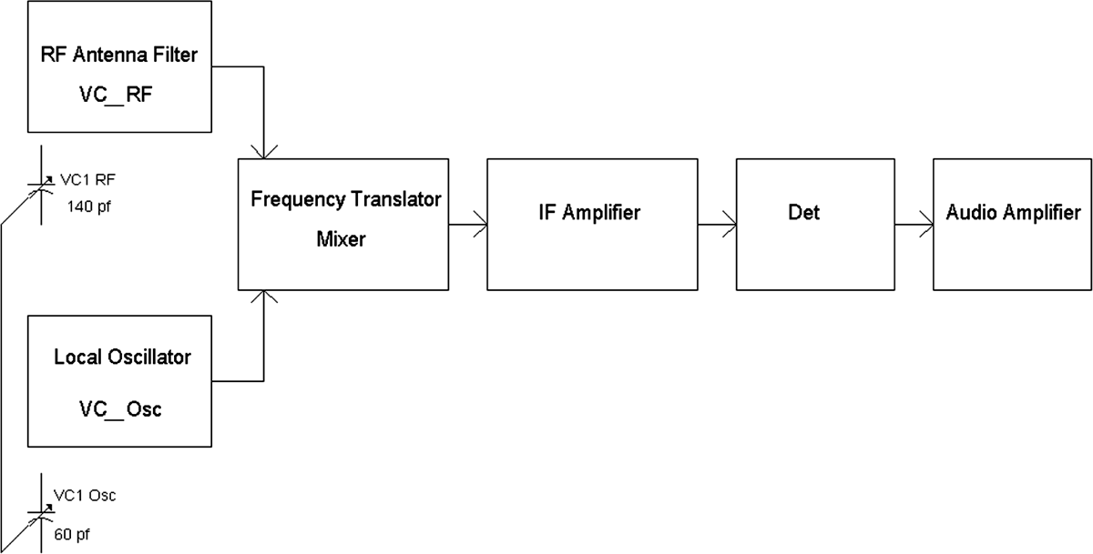
FIGURE 8-1 Block diagram of a superheterodyne receiver.
2. A local oscillator generates a range of frequencies and varies depending on which station is tuned to the AM band. With the ganged variable capacitor, this local oscillator generates a frequency that typically is 455 kHz above the station that is being tuned. For example, when the variable capacitor is at maximum capacitance, the RF filter will be tuned to 540 kHz, whereas the local oscillator will generate a 540 kHz + 455 kHz = 995 kHz signal. Or when the ganged variable capacitor is at a minimum capacitance and is tuned to 1,600 kHz for the RF tunable filter, the local oscillator generates a 1600 kHz + 455 kHz = 2,055 kHz.
3. A mixer circuit really means that there is some type of multiplication of two signals going on. When multiplication occurs in two signals of two different frequencies F1 and F2, the output (of the mixer) will provide signals that have frequencies of (F1 – F2) and (F1 + F2), along with other signals of different frequencies from F1 or F2 as well. This is different from an additive mixer, which simply sums two signals together. In an additive mixer for two signals with frequencies F1 and F2, the output will only give signals of frequencies F1 and F2.
4. The IF filter generally passes a signal whose frequency is the difference frequency of the local oscillator and the incoming RF signal. For example, from element 2, if the radio is tuned to 540 kHz, the local oscillator will be at 995 kHz, and thus the difference between the two frequencies is 995 kHz – 540 kHz = 455 kHz. Similarly, for a radio tuned to 1,600 kHz, the local oscillator will be at 2,055 kHz, so the difference frequency signal will be 2,055 kHz – 1,600 kHz = 455 kHz. An IF filter therefore passes a signal whose frequency is around the IF (e.g., 455 kHz) and attenuates or removes signals whose frequencies are outside the vicinity of the IF. For example, the IF filter also will attenuate the signals from the oscillator and the RF signal input. It should be noted that most superheterodyne radios employ simple mixers that will output sum and difference frequency signals but also will output signals from the local oscillator (1MHz to 2 MHz) and the RF signal input (540 kHz to 1,600 kHz). The (455-kHz) IF filter then also will remove/attenuate signals related to the local oscillator or incoming RF signal.
Commercially Made Transistorized Superheterodyne Radios
One of the first transistor AM radios, the TR-1, was made by I.D.E.A., Inc., Regency Division, in 1955. The circuit topology of the TR-1 followed closely that of the vacuum-tube radios that used converter circuits instead of a separate local oscillator circuit and a mixer circuit (Figure 8-2A).
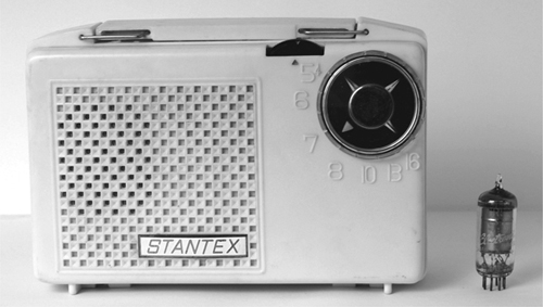
FIGURE 8-2A Portable four-tube radio.
In Figure 8-2B, an antenna coil is connected to a grid of the 1R5 pentagrid (five-grid) converter tube, whereas an oscillator coil is coupled to three grids of the 1R5 tube. Thus the local oscillator’s signal and the incoming RF radio station signal are connected to just one vacuum tube. Connected to the plate of the 1R5 tube is the first IF transformer to extract AM signals that have been “mapped” to 455 kHz.
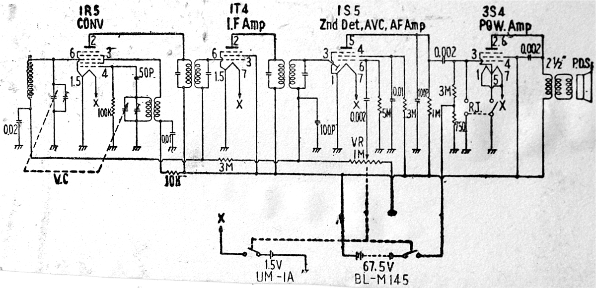
FIGURE 8-2B Schematic diagram of a four-tube radio.
Now let’s turn to a block diagram of a typical transistor radio such as the Regency TR-1 (Figure 8-3).
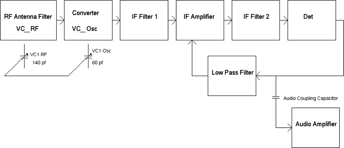
FIGURE 8-3 Block diagram of a four-transistor radio.
The built-in antenna coil and variable capacitor VC_RF tune into a desired radio station to produce an RF signal to the input of the converter circuit. The converter circuit consists of a transistor oscillator circuit in which the oscillation signal is combined with the RF signal. When the two signals, the oscillation signal and the RF signal, are added together, the nonlinear characteristic of the transistor also generates a multiplying action between the two signals. As a result, the output of the converter circuit then produces signals that have frequencies of sums and differences from the RF signal and the oscillation signal.
The output of the converter is connected to IF Filter 1, which only extracts signals that are of the difference frequency. Further amplification of this difference frequency (e.g., 455 kHz) is done with an IF amplifier, and the output of the IF amplifier is connected to a second IF filter.
From the second IF filter comes a 455-kHz AM signal, which is demodulated by an envelope detector (or power detector). The envelope detector performs half-wave rectification on the negative half (lower half) of the AM envelope for two functions. One function is to provide a demodulated AM signal or an audio signal. The second function is to provide a negative direct-current (DC) voltage for automatic volume control (AVC). The negative DC voltage is level shifted up by adding a positive bias voltage such that when a strong signal is received, the net total voltage is a positive voltage that decreases in proportion to signal strength. And when a weak signal is received, the net total voltage is still positive and increases in proportion to the weakness of the received signal.
The DC bias voltage and the half-wave-rectified negative half of the AM envelope are passed through a low-pass filter to remove IF and audio signals, passing only a DC voltage to change the gain of the IF amplifier. For example, for a strong signal received, the constant DC voltage is +1.0 V, and when a weak signal is received, the constant DC voltage is +1.2 V. The AVC system allows a more even audio volume between weak and strong stations received.
To raise the level of the demodulated AM signal, an audio amplifier (AF Amp) is used to supply sufficient signal to drive a loudspeaker or low-impedance earphone. Figure 8-4 provides a more detailed look at the converter circuit.
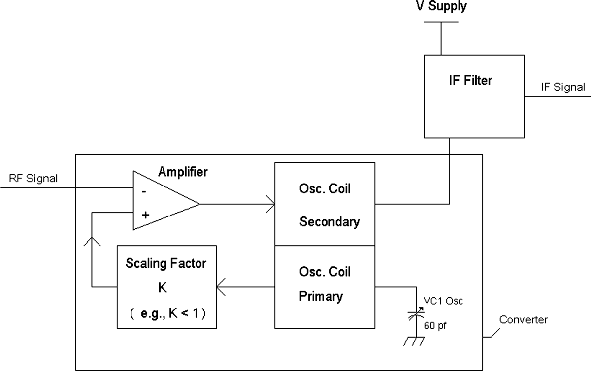
FIGURE 8-4 Block diagram of a converter circuit.
The converter circuit in this figure essentially is an oscillator circuit. Normally, the oscillator circuit has the negative (–) input terminal connected to a voltage source, which is an alternating-current (AC) ground. For now, let’s take a look at just the oscillator section. The output of the amplifier is connected to a secondary winding of the oscillator coil/transformer (e.g., 42IF100). The primary winding of the oscillator coil/transformer has the required inductance with a variable capacitor to span a range of about 1 MHz to 2 MHz for the oscillator signal. The inductance in the primary winding is tapped down to a smaller voltage, as denoted by the K, a scaling factor of less than 1. The tapped-down signal then is connected to the positive input terminal of amplifier to form a deliberate positive-feedback system so as to provide oscillation.
With the circuit oscillating, the transistor is driven with a relatively large oscillating signal voltage at the positive (+) terminal, usually greater than a 200-mV peak-to-peak sine wave. This large signal also causes the transistor amplifier to distort and produce harmonic distortion at the output of the amplifier. When a low-level RF signal from the antenna coil is combined with the amplifier via its negative (–) input terminal, the combination of an RF signal and an oscillating signal produces intermodulation distortion signals at the output of the amplifier. A couple of the intermodulation distortion signals happen to have frequencies that are the sum and difference frequencies of the RF signal and the oscillating signal. These intermodulation distortion signals are attenuated (e.g., ignored) by the oscillator’s tank circuit and do not affect the oscillator. But one of these intermodulation distortion signals is extracted via an IF filter tuned to the difference frequency or the IF frequency. And the output of the IF filter then is connected to the input of an IF amplifier (not shown).
A Four-Transistor Radio Schematic
In 1955, the Regency TR-1 was the first commercially manufactured superheterodyne radio. It used four transistors for the following functions: the converter, the first IF amplifier, the second IF amplifier, and the audio amplifier. This radio ran off a 22.5-volt battery, which was common back then and up to the 1970s but is rare today.
For our first superheterodyne radio, we shall use a 1.5-volt to 3-volt source instead a 22.5-volt battery as well as four transistors, but as the converter, the IF amplifier, the audio driver, and the audio power amplifier.
Parts List
• C1, C4, C10: 33 μF, 16 volts
• C2, C6, C9, C13: 0.01 μF
• C3, C7, C8: 1 μF, 35 volts
• C5: 0.15 μF
• C11, C12: 220 μF, 16 volts
• R1: 3,300 ![]()
• R2: 2,200 ![]()
• R3: 1 k![]()
• R4: 10 k![]()
• R5, R6: 20 k![]()
• R7: 470 ![]()
• R8: 20 ![]()
• VR1: 100 k![]()
• D1, D2, D3, D4: 1N914
• Q1, Q2, Q3, Q4: 2N3904
• L1 antenna coil: primary 600 μH to 680 μH, secondary 10 to 20 turns
• T1 oscillator coil: 42IF100
• T2 IF transformer: 42IF101
• T3 IF transformer: 42IF103
• T4 audio driver transformer: primary 10 k![]() CT, secondary 600
CT, secondary 600 ![]() CT or primary 2.5 k
CT or primary 2.5 k![]() , secondary 600
, secondary 600 ![]() CT
CT
• T5 audio output transformer: primary 120 ![]() , secondary 8
, secondary 8 ![]()
• VC1: 140 pF RF and 60 pF oscillator
Figure 8-5A shows a block diagram of the four-transistor radio, and Figure 8-5B shows the schematic of the four-transistor radio.

FIGURE 8-5A Block diagram of a four-transistor radio.
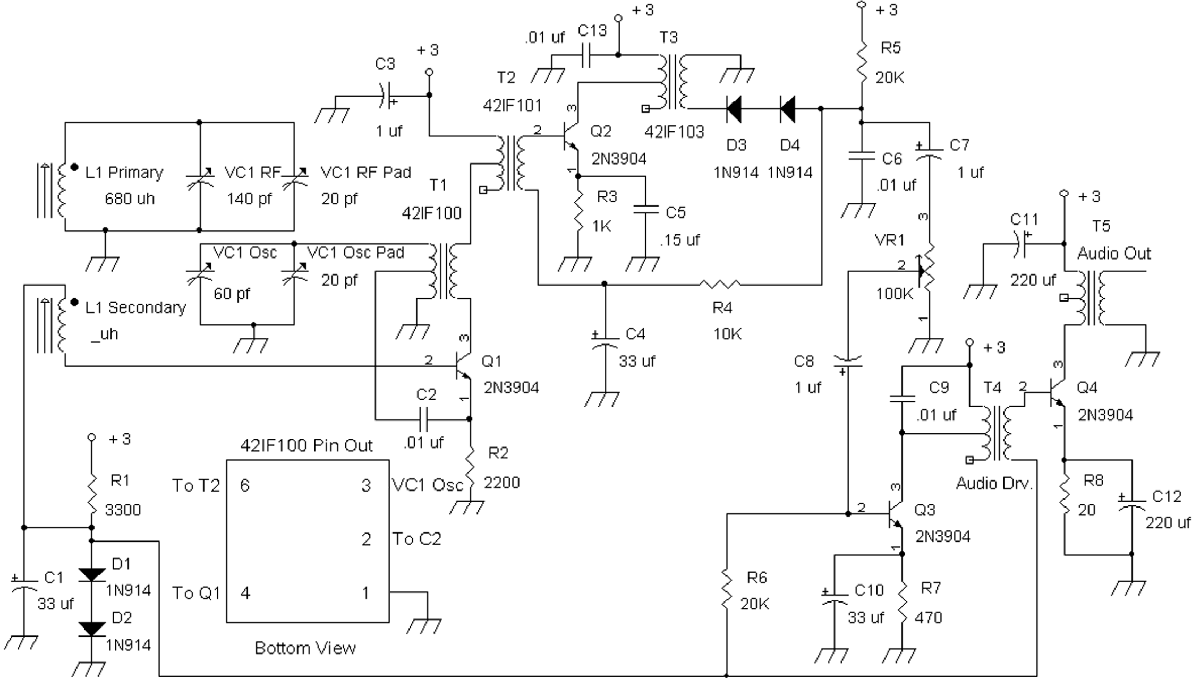
FIGURE 8-5B Schematic diagram of a four-transistor radio.
Radio signals are received via antenna coil L1. L1 resonates with variable capacitor VC1_RF. The tuned RF signal is stepped down via the L1 secondary winding, which is connected to the base of Q1, an oscillator circuit. Oscillator coil T1 has a secondary winding that serves as a tickler winding to couple the output signal from the collector of Q1 back to the input emitter of Q1 to form a positive-feedback system that ensures oscillation. The primary winding of T1 is connected to the second gang or section of variable capacitor VC1_Osc to allow varying the oscillation frequency in the range to 1 MHz to 2 MHz. It should be noted that the primary winding of T1 has a tapped winding that is connected to the emitter of Q1 via capacitor C2. The tapped winding allows connection to the low-input resistance at the emitter of Q1, which is typically less than 500 V to avoid degrading the Q of the parallel resonant tank circuit, consisting of the inductance in the primary winding of T1 and capacitor VC1_Osc. The base of Q1 is biased by diodes D1 and D2 to provide a DC bias voltage at the base of Q1 of about 1 volt, which also sets the DC collector current for Q1. R2 is chosen to set a sufficient emitter current (e.g., ~200 μA) to provide enough voltage gain in transistor Q1 to reliably produce oscillation.
Because the secondary winding of L1 provides the RF signal to the base of oscillator transistor Q1, multiplication of the oscillator signal with the RF signal occurs. And the output signal at the collector of Q1 includes an amplified frequency-translated signal version of the RF signal to 455 kHz.
Note that T2, the first IF transformer’s primary, via its tapped winding is in series with the secondary winding of T1, the oscillator coil. By this series connection, the 455-kHz (IF) signal is extracted from the collector of Q1.
The secondary winding of T2 is also stepped down to allow connection to the base of the IF amplifier’s transistor Q2, which has a moderate input resistance (e.g., in the few thousands of ohms) so as not to degrade the Q at the primary of T2.
At the output of the IF amplifier’s transistor Q2, the collector is connected to the second IF transformer. The AM signal from second IF transformer’s secondary is demodulated via diodes D3 and D4. One may ask why two diodes in series? The second diode performs the function of level shifting up the voltage by about 0.5 volt DC, which is needed in an automatic volume-control system with transistor Q2. Thus diodes D3 and D4 perform envelope detection, and through biasing resistor R5, the two diodes also level shift the detected lower half of the AM envelope to a voltage of about 1 volt DC when the RF signal is zero or weakly received. This 1-volt signal is further filtered by R4 and C4 and applied to the secondary winding of T2 to bias the IF transistor Q2. When a signal is received, the demodulated signal at C6 is sitting at 1 volt DC with a negative-going AC audio signal. Low-pass filter R4 and C4 filter out the AC audio signal and provide a DC voltage that is 1 volt minus the average carrier level of the received signal. The stronger the received RF signal, the more the average carrier level is “subtracted” from the 1-volt DC signal at C4. By lowering the biasing voltage for Q2 depending on how strong the received signal is, Q2 performs an automatic gain or volume control for the demodulated audio signal. Note that if there were only one diode instead of D3 and D4, maximum DC voltage would be 0.5 volt, which is insufficient to turn on the base of Q2 (e.g., Q2 requires at least 0.6 volt on the base).
It should be noted that the second IF transformer here or, in general, the last IF transformer before diode detection usually has a lower turn ratio from primary to secondary windings compared with any of the other IF transformers. The reason is to provide more IF signal to the diode detector, which also generates sufficient AVC voltage. For example, if T3 is changed from a 42IF103 part to a 42IF101 or a 42IF102 transformer (both with about a 20:1 turns ratio) instead, there will be lower amplitude-demodulated signals (compared with the 42IF103 transformer with a 6:1 turns ratio) because of the higher turns ratio in these two parts, which then results in insufficient AVC voltage for good automatic volume control.
The demodulated signals from D4 are AC-coupled to the base of the audio driver transistor Q3 via volume control VR1. The output of Q3 is connected to an interstage step-down transformer T4 (2.5-k![]() primary to 150-
primary to 150-![]() secondary) to generate increased current drive into output audio transistor Q4. Transistor Q4 is biased at about 20 mA, which results in an input resistance of about 130
secondary) to generate increased current drive into output audio transistor Q4. Transistor Q4 is biased at about 20 mA, which results in an input resistance of about 130 ![]() to 150
to 150 ![]() at the input of Q4. The amplified audio signal via Q4’s collector is connected to step-down transformer T5 to drive a speaker or low-impedance earphone.
at the input of Q4. The amplified audio signal via Q4’s collector is connected to step-down transformer T5 to drive a speaker or low-impedance earphone.
Although this radio runs off two cells for 2.4 volts to 3 volts, it will operate down to 1.2 volts as well. Because of the current drain of this radio, a power switch in series with the battery is suggested.
An Eight-Transistor Radio
For designing an eight-transistor radio, a more “traditional” approach was taken. That is, in most common descriptions of a superheterodyne radio, there is a tuned RF circuit, a separate local oscillator, a mixer, IF filters and amplifier(s), a detector, and the audio amplifier (Figure 8-6A).
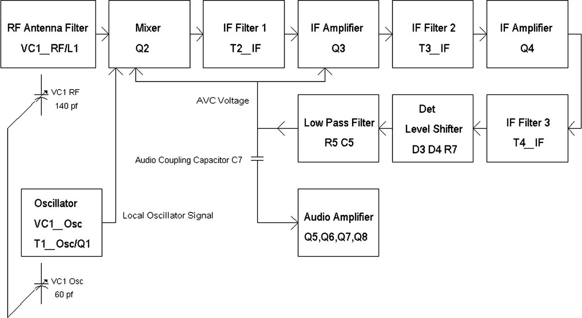
FIGURE 8-6A Block diagram of an eight-transistor radio.
In Figure 8-6A we see that there is a ganged variable capacitor for the tuned RF stage and local oscillator. The antenna coil receives radio stations via magnetic energy and resonates or tunes with the RF section of the variable capacitor. RF signals from the antenna coil are connected to an input of the mixer circuit. The local oscillator is also connected to the mixer circuit such that there is a combination of both RF and oscillator signals at the input(s) of the mixer. Because the oscillator’s signal into the mixer is very large, the mixer generates intermodulation distortion products at its output. It should be noted that the intermodulation distortion products or signal from the mixer also can be thought of as a result of the oscillator signal multiplying with the RF signal. And one of the intermodulation distortion products is a frequency-translated version of the RF signal to an IF such as 455 kHz. Thus the first IF filter extracts the 455-kHz signal from the output of the mixer.
Signals from the first IF filter are amplified by the first IF amplifier. The output of the first IF amplifier Q3 is connected to a second IF filter, and the output of the second IF filter is further amplified by a second IF amplifier Q4. Finally the output of the second amplifier is connected to a third IF filter. From the third IF filter, demodulation occurs via a detector circuit. But also from the detector circuit is a DC level-shifting circuit that is connected to a low-pass filter with a resistor capacitor (RC) time constant of 0.1 second to 0.5 second. The output of the low-pass filter then provides an AVC voltage, which controls the conversion gain of the mixer circuit and the voltage gain of the first IF amplifier. By having gain control over two stages, the mixer and first IF amplifier, there is more AVC range compared with applying an AVC voltage to one stage such as the previously described four-transistor radio.
An audio driver stage amplifies the demodulated AM signal with sufficient current drive to a push-pull audio amplifier for listening via a loudspeaker or low-impedance earphone.
Parts List
• C1, C6, C8: 0.15 μF
• C2, C5, C12, C15: 33 μF, 16 volts
• C3, C4, C7, C9, C18, C19, C20: 0.01 μF
• C10, C11, C17: 1 μF, 35 volts
• C13, C14, C16: 220 μF, 16 volts
• R1, R13: 2,200 ![]()
• R2, R4, R6: 1,000 ![]()
• R3, R10: 4,700 ![]()
• R5, R12: 10 k![]()
• R7, R8: 20 k![]()
• R9: 100 k![]()
• R14: 3.0 ![]()
• D1, D2, D3, D4, D5: 1N914
• D6: 1N270 or 1N34
• Q1 to Q8: 2N3904
• L1 antenna coil: 600 μH to 680 μH with tap or secondary winding
• VC1 variable capacitor: 140 pF and 60 pF
• T1 oscillator coil: 42IF100
• T2 IF transformer: 42IF101
• T3 IF transformer: 42IF102
• T4 IF transformer: 42IF103
• T5 audio transformer: primary 1.5 k![]() , secondary 600
, secondary 600 ![]() CT
CT
• T6 audio transformer: primary 48 ![]() CT, secondary 8
CT, secondary 8 ![]()
• VR1: 100 k![]()
Figure 8-6B presents a schematic diagramof the tuner section of the eight-transistor radio, while Figure 8-6C presents a schematic diagram of the audio section of the eight-transistor radio.
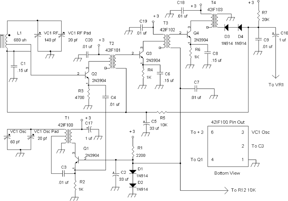
FIGURE 8-6B Schematic diagram of the eight transistor radio’s tuner section.
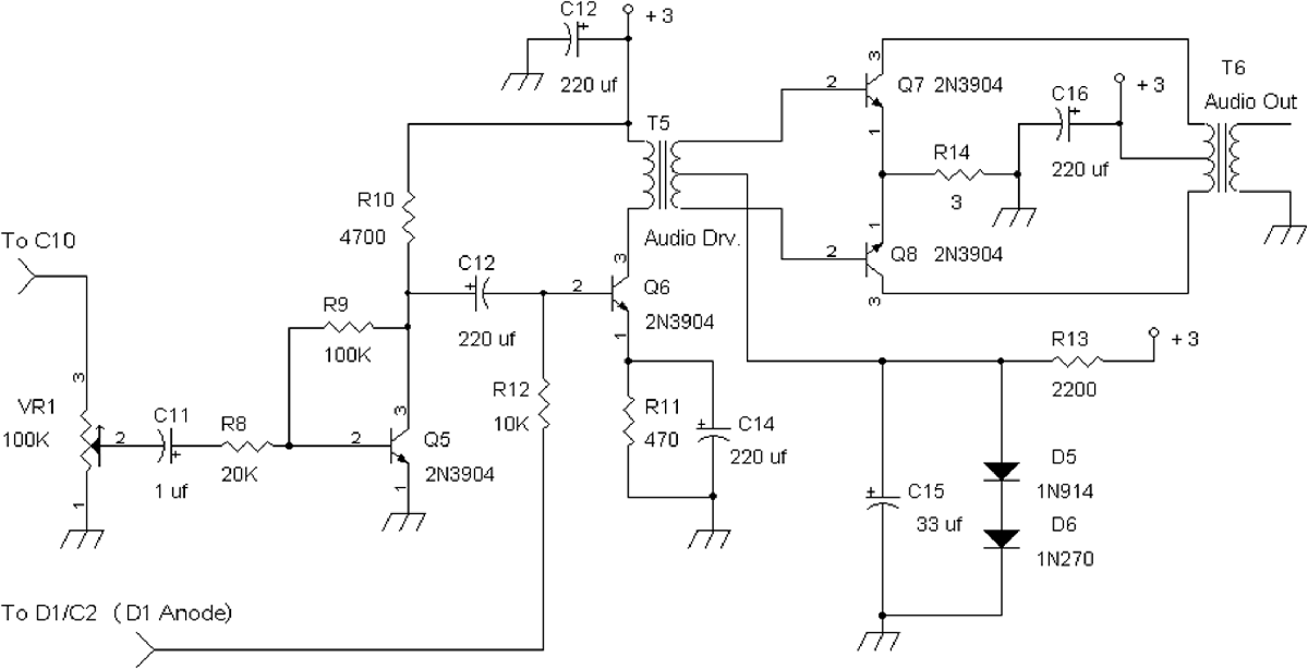
FIGURE 8-6C Audio amplifiers for the eight transistor radio.
Oscillator circuit Q1 generates a 1-MHz to 2-MHz signal of more than 300 mV (peak-to-peak sine wave) at its emitter via oscillator coil T1 and variable capacitor VC1_Osc. Positive feedback is established by coupling the output signal from the collector of Q1 back to its emitter terminal via a tapped winding from T1’s primary winding. The oscillation signal at the emitter then is connected to the emitter (input) of mixer circuit Q2. Low-level RF signals are connected to the base input terminal of the mixer Q2 via a tap in antenna coil L1. As stated earlier, VC1_RF tunes with the antenna coil (680 μH) to resonate or give maximum signal level when tuned to a radio station.
At first glance, it looks as though the signal at the collector of mixer transistor Q2 will be an amplified version of the two signals, the low-level RF signal and the oscillator signal, connected to its inputs. But because the oscillator signal’s amplitude is very large, Q2 is driven into deliberate distortion, which causes its output at the collector to generate signals that are the sum and difference frequencies of the low-level RF signal (540 kHz to 1,600 kHz) and the oscillator signal (1 kHz to 2 MHz), as well as providing amplified versions of the RF and oscillator signals. However, because the difference frequency signals (e.g., IF signals) are at 455 kHz and all other signals are at frequencies above 455 kHz, the first IF filter, T2, is able to extract the IF signal and reject all the other signals from the mixer’s output.
The extracted IF signal from the secondary winding of T2 is amplified by the first IF amplifier Q3 via a connection to the base of Q3. The amplified signal from the collector of Q3 is then connected to a second IF filter T3 for further band-pass filtering around 455 kHz. A second-stage IF amplifier Q4 further amplifies signals from the secondary winding of T3. A third IF filter T4 is connected to the output of Q4. Demodulation of the 455-kHz signal at the secondary winding of T4 is done by diodes D3 and D4, which also provide a DC level-shifted voltage of the demodulated signal. The demodulated and DC level-shifted signal is further low-pass filtered to remove audio information via R5 and C5. Thus the voltage at C5 represents a DC shifted-voltage version of the average RF carrier level of the signal from the radio station. And thus this voltage at C5 provides an AVC voltage that is connected to the bases of Q2 and Q3 via the secondary winding of L1 and primary winding of T2. Since both bases of Q2 and Q3 require at least 0.6 volt of biasing voltage, the voltage from D3, D4, and R7 provides about 1.0 volt of DC to start with that allows biasing of Q2 and Q3.
Automatic volume control then is accomplished by varying the signal output from mixer 2 and first IF amplifier Q3 in an inverse manner. The higher the received signal, the lower is the AVC voltage to turn down the gain. Conversely, the lower the received signal, the higher is the AVC voltage to turn up the gain.
The demodulated signal from D4 is further audio amplified by Q5 and Q6, and its volume is controlled by VR1. Amplifier Q5 is an inverting-gain amplifier that is connected to a driver amplifier Q6. The output of amplifier Q6 is connected to an interstage transformer T5 to boost the audio signal current into transistors Q7 and Q8 in a push-pull manner. The phase of the audio signal into the base of Q7 is 180 degree in reference to the phase of the audio signal at Q8. Biasing of Q7 and Q8 is accomplished by the voltage generated by diodes D5 and D6 and R13. Signal currents in a push-pull manner from Q7 and Q8 are connected to output transformer T6 so that its secondary winding can drive a loud speaker or low-impedance earphone.
This radio will work fine off 2.4 volts to 3 volts but also will run off 1.2 volts. Also because of the current drain, a power switch in series with the battery is suggested.
Alternative Oscillator and Antenna Coil Circuit
In Chapter 3 it was noted that one of the sections of a twin variable capacitor can be used for the oscillator circuit. A series capacitor of 110 to 120 percent of the variable capacitor’s maximum capacitance in an oscillator circuit allows for accurate tracking with the tuned RF stage. For example, with a twin variable capacitor of 270 pF, a 330-pF series capacitor is needed for the oscillator circuit. And for a twin 335-pF variable capacitor, a 390-pF series capacitor is required. Figure 8-7 shows an alternative oscillator and antenna coil circuit for the eight-transistor radio.

FIGURE 8-7 Alternative tuner section for the eight-transistor radio.
In this circuit, instead of using a nonsimilar two-gang variable capacitor for the tuned RF and oscillator circuit, a twin 270-pF variable capacitor is used. Twin variable capacitors are used not only for superheterodyne radios covering the broadcast AM band or medium-wave band, but they are also used for long- and short-wave radio bands as well.
For an AM radio with a twin 270-pF capacitor with a series 330-pF capacitor C16, we need about 140 μH of inductance. Because the 42IF100 oscillator coil T1 has nominally about 330 μH, a 220-μH or 270-μH fixed inductor is paralleled with the main primary winding of T1 to provide a net inductance of about 140 μH. Also, a fixed 15-pF capacitor C22 is paralleled with the primary winding of T1 or with L2 for better tracking with the tuned RF stage. In addition, the emitter resistor R2 (for the oscillator circuit Q1) is changed from 1 k![]() to 510 to ensure more than 300 mV peak to peak of the oscillation signal (at Q1’s emitter). Note that C3 is connected to the low-side tap of T1. The output of the oscillator is connected to mixer transistor Q2’s emitter terminal through C4.
to 510 to ensure more than 300 mV peak to peak of the oscillation signal (at Q1’s emitter). Note that C3 is connected to the low-side tap of T1. The output of the oscillator is connected to mixer transistor Q2’s emitter terminal through C4.
As mentioned in Chapters 3 and 5, using a loop antenna allows for more flexibility because loop antennas can be made with about 10 turns around a 6-inch rectangle, square, or ellipse or bought readily at MCM Electronics or on the Web. Thus a loop antenna is connected to a second 42IF100 coil T7; it is connected to the low-side tap that is used as an RF transformer. The other section of the twin 270-pF variable capacitor is connected to the main primary winding of T7, whereas the secondary winding of T7 provides RF signals to the mixer transistor Q2 via its base terminal. And for automatic volume control, one side of the secondary winding of T7 is connected to the AVC voltage source at C5. Figure 8-7 shows the alternative oscillator and antenna coil circuit, including part of the mixer circuit Q2 and first IF amplifier circuit Q3. This circuit can be “dropped in” or substituted for the oscillator and tuned RF section circuits of the eight-transistor radio circuit shown in Figure 8-6B.
Figure 8-8 shows another type of oscillator, a differential-pair transistor oscillator.
As stated earlier, the loop antenna is connected to the low-side tap of T7 (42IF100).
It was found that an IF transformer (the 42IF104) has about 140 μH from the low-side tap of its primary winding. Because of interelectrode capacitances of the oscillator transistor, it is undesirable to connect this low-side 140-μH tap directly to a transistor. Instead, therefore, the stepped-down secondary winding is used. At resonance, resistance “looking” into the 140-μH tap is very high, on the order of 100 kV or more, but looking into the secondary, this 100 k![]() gets divided by N × N, where N is the turns ratio from the low-side tap to the secondary winding. For the 42IF104, N is in the range of about 14, which means that at resonance the equivalent resistance across the secondary winding is about 500
gets divided by N × N, where N is the turns ratio from the low-side tap to the secondary winding. For the 42IF104, N is in the range of about 14, which means that at resonance the equivalent resistance across the secondary winding is about 500 ![]() (100 k
(100 k![]() divided by 142).
divided by 142).
The differential-pair transistor oscillator is formed by Q1A and Q1B. The collector of Q1A is connected to the secondary winding of the 42IF104 IF transformer, which is like a 500-![]() load. To ensure oscillation by positive feedback, the collector of Q1A is connected to the base of emitter follower transistor Q1B, where its emitter is connected back to the emitter of Q1A. With sufficient DC collector currents set for both transistors, there will be enough gain to sustain a reliable oscillation. And the oscillator’s signal is taken from the collector of Q1A and added in series with the RF signal via the secondary winding of T7.
load. To ensure oscillation by positive feedback, the collector of Q1A is connected to the base of emitter follower transistor Q1B, where its emitter is connected back to the emitter of Q1A. With sufficient DC collector currents set for both transistors, there will be enough gain to sustain a reliable oscillation. And the oscillator’s signal is taken from the collector of Q1A and added in series with the RF signal via the secondary winding of T7.
It should be noted that the mixer circuit is modified slightly by grounding the emitter of Q2 with a 0.15-μF capacitor and summing both oscillator and RF signals into the base of Q2. Again, the oscillator signal is large enough to cause a modulation or multiplying effect on the RF signal from the secondary winding of T7. Thus the output signal from Q2’s collector into the IF filter, T2, is a 455-kHz AM signal.
The AVC voltage from C5 is sent to the base of Q2 via resistor R20 and to the base of the IF amplifier transistor Q3 via the secondary winding of the second IF transformer T2 (42IF102). As we will see in Chapter 9, the differential-pair oscillator will play an important role in low-powered oscillator circuits.
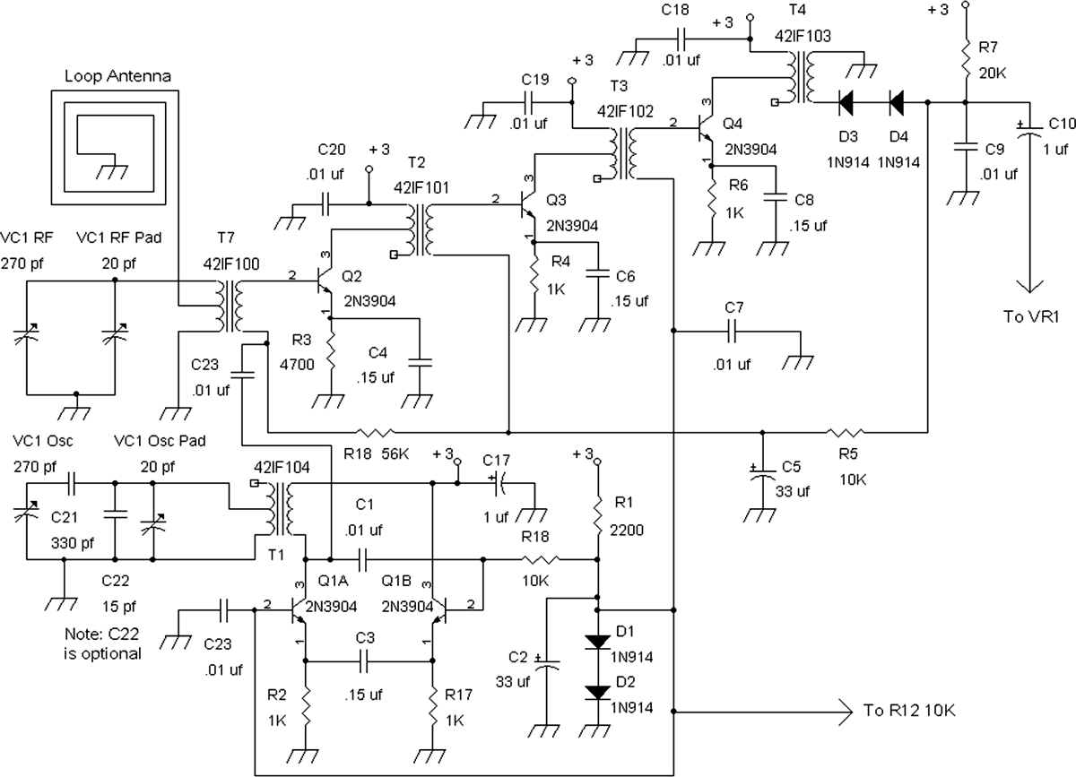
FIGURE 8-8 Differential-pair oscillator (Q1A, Q1B) for alternative tuner section of the eight-transistor radio.
An Item to Note
Generally, the 42IF100 oscillator coil can be substituted with the 42IF300 or the 41IF110 for use as an RF transformer (with a loop antenna) or as an oscillator coil. However, some experimentation may be needed to achieve equivalent results to the 42IF100. For example, in an oscillator circuit, the converter or oscillator transistor’s emitter resistor may have to be reduced in value (e.g., in half) or increased (e.g., up to twofold) when substituting the 42IF300 or 42IF110 for the 42IF100 coil.