Chapter 13
Oscillator Circuits
In Chapters 8, 9, and 10, oscillator circuits were used as local oscillators and converters (mixer and oscillator combination). In this chapter we will explore some “simple” analyses of a one-transistor oscillator circuit and a differential-pair oscillator. Both of these types of inductor/capacitor (LC) circuits have been used in some of the superheterodyne radio designs, and in a sense, this chapter is a “tutorial” on how these circuits work in more detail.
Although the oscillator circuits presented in this chapter are “simplified” for analysis sake and for ease of building and experimentation, the basic oscillator principles still apply. For example, the one-transistor circuit will use capacitors for “stepping down the voltage” instead of an oscillator coil/transformer.
The objectives for the analysis of oscillator circuits are as follows:
1. Introduce the reader to transconductance, which is related to the voltage-to-current gain.
2. Show how transconductance determines whether a circuit will oscillate reliably.
3. Illustrate that there are two types of transconductances—small-signal transconductance and large-signal transconductance.
4. Explain the role of the inductor and capacitors used in the oscillator circuit to determine oscillator frequency and equivalent turns ratio for a transformer.
But first let’s take a systems approach to how oscillators work in general.
A condition for oscillation includes the following characteristics:
1. The total gain from the amplifier to the LC circuit and back to the input of the amplifier must exceed 1; typically, the gain is at least 2.
2. The total phase shift around the system must total to 0 or 360 degrees. So, if the amplifier has an inverting gain (e.g., common-emitter amplifier), the other components must deliver 180 degrees of phase shift. And if the amplifier has a noninverting gain (e.g., common or grounded-base amplifier), the other components typically must have a net phase shift of 0 degree.
Figure 13-1 shows an oscillator system. A gain amplifier’s output terminal is connected to a resonant filter, and the output of the resonant filter is fed back to the input terminal of the gain amplifier. The filter is commonly implemented as a parallel LC circuit.
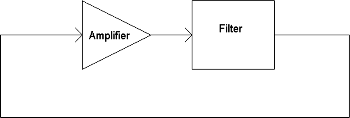
FIGURE 13-1 Basic oscillator system.
The filter in the figure is usually a parallel LC circuit of some kind that has 0-degree phase shift at its resonant frequency of 1/2π ![]() . At a frequency above the resonant frequency, the phase shift usually lags or creates a negative phase shift. Above the resonant frequency, the LC network has more capacitive characteristics than inductive or resistive. And at frequencies below the resonant frequency, the LC network has more inductive characteristics that cause a phase lead or positive phase shift.
. At a frequency above the resonant frequency, the phase shift usually lags or creates a negative phase shift. Above the resonant frequency, the LC network has more capacitive characteristics than inductive or resistive. And at frequencies below the resonant frequency, the LC network has more inductive characteristics that cause a phase lead or positive phase shift.
In an oscillator system, the positive-feedback mechanism responsible for causing the oscillation will readjust itself to shift the frequency of the oscillator to maintain the 0-degree phase shift. In a sense, the oscillator “servos” itself to correct for 0 degrees by readjusting its frequency.
So, for example, what if the gain amplifier in Figure 13-1 has some phase lag owing to a roll-off in frequency response, which causes a negative phase shift? The oscillator system is pretty “smart”; it lowers the frequency of the oscillation signal so that the LC filter is below the original resonance frequency, which, in turn, causes a phase lead to cancel out the phase lag of the amplifier. As a result, the oscillator will run at a lower frequency. This makes sense because a slower amplifier (see Figure 13-1) causes an oscillator to run slower in the form of a lower frequency.
The filter is commonly implemented as a parallel LC circuit (Figure 13-2). A voltage-driven LRC circuit can be used, such as the oscillator used in the SDR frontend circuit in Figure 13-3, U1A. Alternatively, and more commonly, the LRC circuit is driven with a current source via the collector of a transistor, although there are exceptions where the emitter drives an LC or LRC circuit to form an oscillator (Figure 13-4).
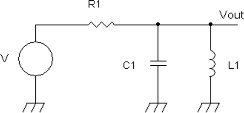
FIGURE 13-2 An LRC circuit that is voltage driven.

FIGURE 13-3 Schematic diagram of an AM radio front-end circuit for an SDR that includes a commutating mixer.
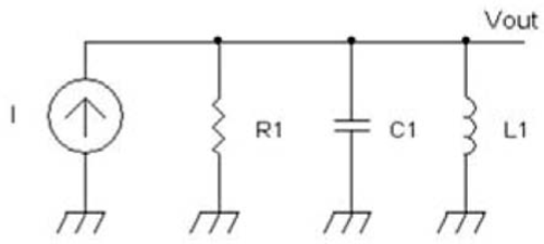
FIGURE 13-4 A current-driven LRC circuit.
Many active devices have current-source outputs such as a bipolar transistor with a collector terminal or a field-effect transistor with a drain terminal. The concept of a current source may not be familiar to some people because a voltage source is more easily visualized as a battery or a signal generator. In an ideal voltage source, the generated signal delivers a voltage signal independent of the current flowing into or out of the voltage source. In an ideal current source however, the generated current is independent of the voltage across the ideal current source.
One-Transistor Oscillator
Figure 13-5 shows an oscillator system with a voltage-dependent current source. The current source is controlled by the amount of voltage applied to the input of the system. Signal current is fed to a parallel LC circuit where two capacitors form a voltage divider network.

FIGURE 13-5 An oscillator system using a voltage-controlled current source.
The resonant frequency is still ![]() , where C = C1 × C2/(C1 + C2). Moreover, since C1 and C2 form a voltage divider, the capacitive voltage divider acts pretty much like a step-down transformer in terms of a turns ratio of 1/n = C1/(C1 + C2). The voltage-controlled current source is a transconductance device, which means that a change in input voltage results in a change in output current. Or, equivalently, the transconductance of a device = ΔIout /ΔVin, which can be construed as the ratio of
, where C = C1 × C2/(C1 + C2). Moreover, since C1 and C2 form a voltage divider, the capacitive voltage divider acts pretty much like a step-down transformer in terms of a turns ratio of 1/n = C1/(C1 + C2). The voltage-controlled current source is a transconductance device, which means that a change in input voltage results in a change in output current. Or, equivalently, the transconductance of a device = ΔIout /ΔVin, which can be construed as the ratio of
![]()
So now let’s take a look at a particular transconductance device—the bipolar transistor. This transistor can be approximated by a part of the Ebers-Moll equation:
![]()
where Is is the transistor’s reverse bias saturation current or leakage current (e.g., 0.01 pA to 0.0001 pA), VBE is the base-to-emitter voltage, e = 2.71828..., and (KT/q) = VT = 0.026 volt direct current (DC) at room temperature. VT is also known as the thermal voltage.
The small signal transconductance of the bipolar transistor at a particular DC collector current ICQ is given by

If we did not know about Equation (13-2), there is another way to indirectly come up with the transistor’s transconductance by plugging values into Equation (13-1). For Table 13-1, Is = 0.01 pA. Note that the transconductance is independent of the value of Is.
TABLE 13-1 Calculated Small Signal Transconductances of a Bipolar Transistor
From this table, one can see that Equation (13-2) is valid and that the small-signal transconductance is linearly proportional to the DC collector current. And, as seen from Equation (13-2), it is valid for calculating the small-signal transconductance of a bipolar transistor. And by small signal, we are limiting the alternating-current (AC) signal into the base emitter of the transistor to about 5 mV to 15 mV peak to peak.
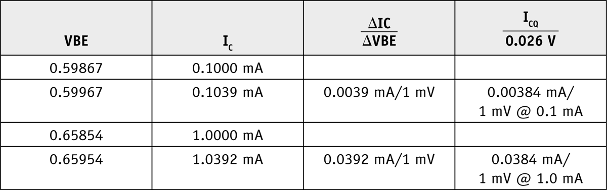
If the base-emitter AC signal is larger than 15 mV peak to peak, gross distortion will occur at the output of the collector, and a large-signal transconductance model will have to be used. For example, Figure 13-6 shows an input signal at the base and emitter of a transistor of about 5 mV peak (10 mV peak to peak) and 39 mV peak (78 mV peak to peak). As can be seen in the figure, for small input signals, the collector current output looks pretty much like a sine wave, but for large input signals, the collector current is larger in amplitude but highly distorted.
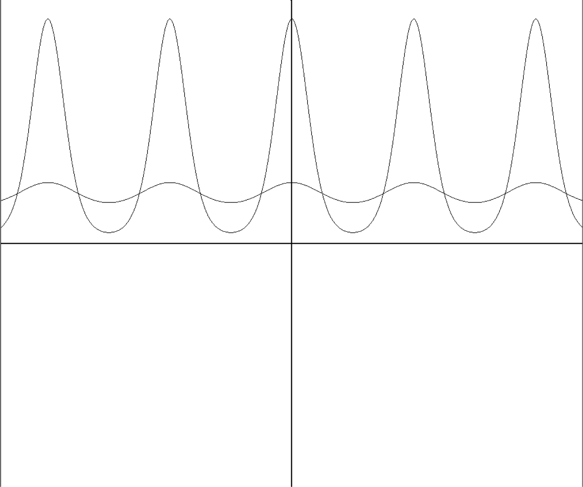
FIGURE 13-6 Output collector current for small and large input sinusoidal signals at the base-emitter junction of a transistor. The X axis is time, and the Y axis is the output current.
When an output signal gets distorted, harmonics are generated, and as the input signal level is increased, the fundamental frequency signal at the output is no longer proportional to the input signal’s amplitude. Thus the output level of the fundamental frequency signal gets compressed (Figure 13-7). In the figure, the straight line shows the input signal increasing linearly, whereas the output starts to compress.
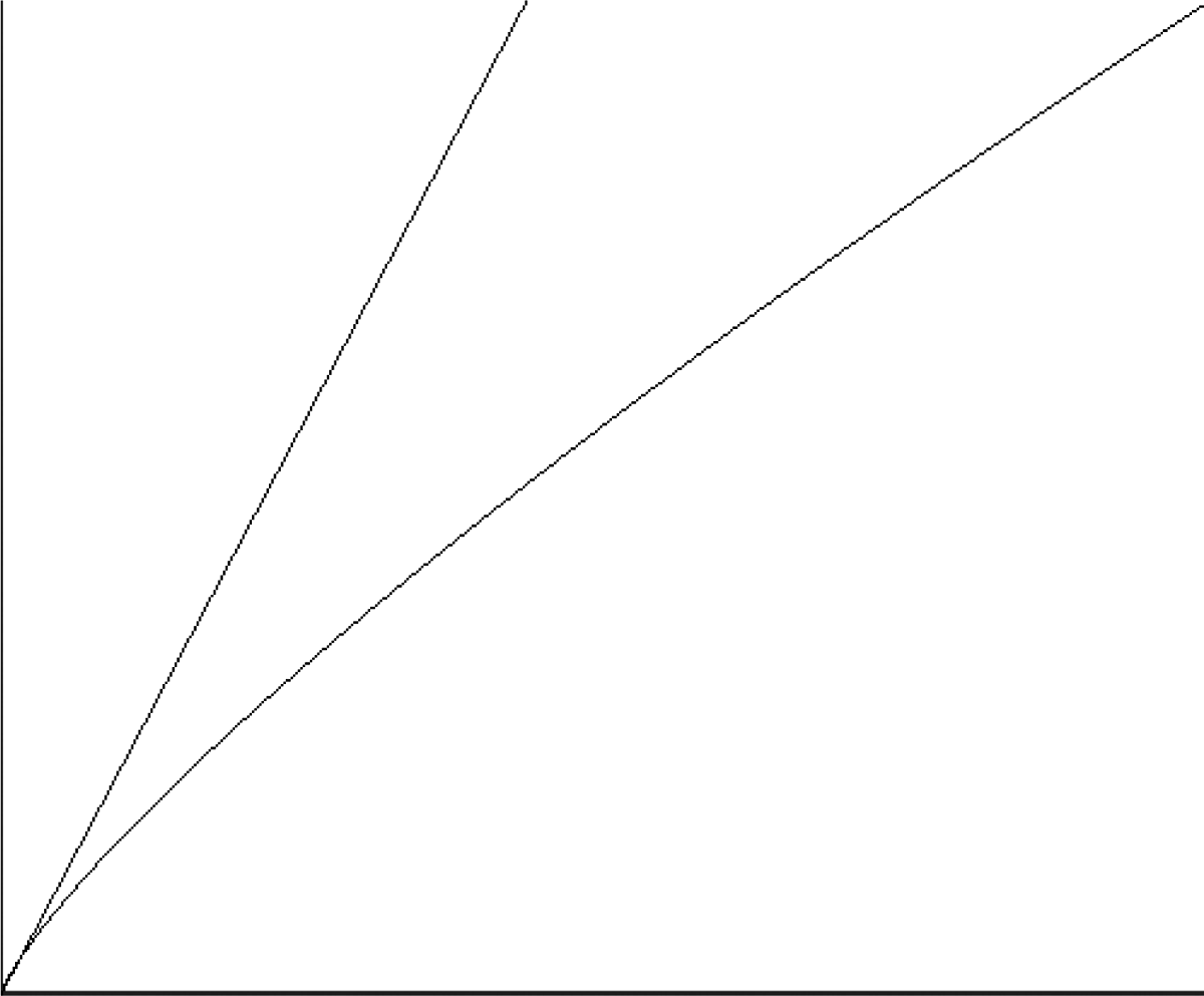
FIGURE 13-7 Example of gain or transconductance compression. The X axis is the input, and the Y axis is the output.
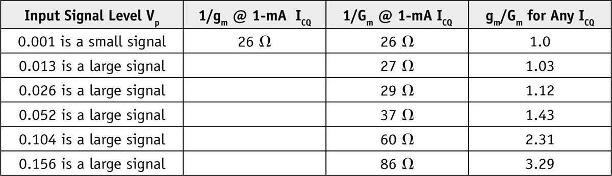
So let’s take a look at how the large-signal transconductance Gm is different from the small-signal transconductance gm measured in amperes per volt for a DC collector current of 1 mA = ICQ for various sine-wave amplitudes measured at a peak voltage Vp or as a function of sin(ωt) into the base-emitter junction of the transistor (Table 13-2). And the output collector current is the amplitude of the signal current at only the fundamental frequency. Note that ICQ is the quiescent (DC) collector current.
TABLE 13-2 Comparisons of Large and Small Signal Transconductances as a Function of Base-Emitter Peak Sine Wave Driving Voltages

See Figure 13-8 for input signals of 26 mV peak and 52 mV peak. Note that as the input signal is increased with a sinusoid, the collector output gets narrower, approaching a delta pulse as the input keeps on increasing. The spectrum of the narrow pulse contains fundamental and harmonic frequencies, with the amplitude of the harmonic signals being close to the amplitude of the fundamental frequency signal (Figure 13-8).
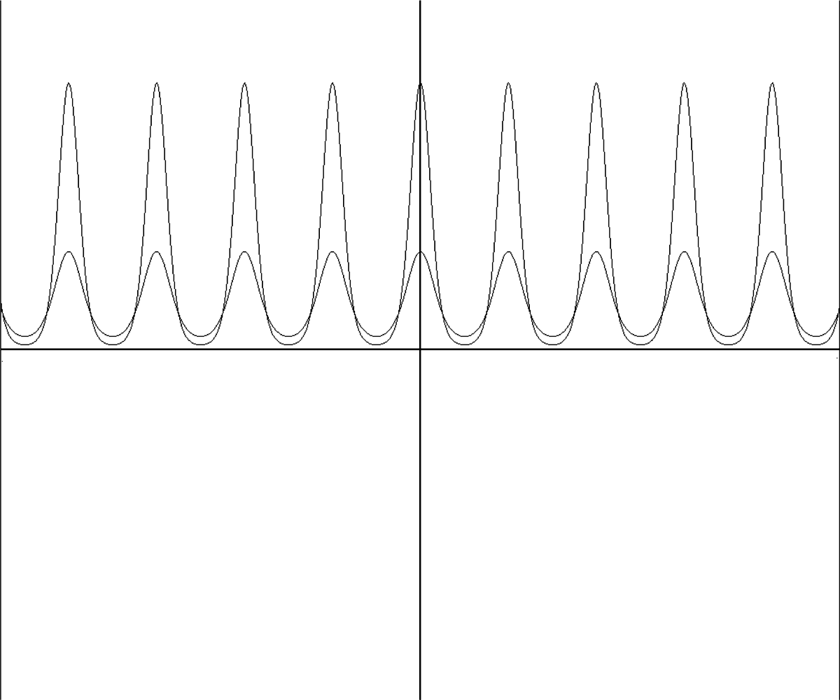
FIGURE 13-8 Output current of a transistor with 26-mV peak and 52-mV peak AC signals at the input. The X axis is time, and the Y axis is the output current.
From Figures 13-6 through 13-8 we see that when the input of a bipolar transistor amplifier is overdriven with a large signal, there is a lowering of effective transconductance pertaining to signals with the fundamental frequency. So how does this lowering of the effective transconductance of the transistor owing to overloading affect other characteristics such as input resistance in a bipolar transistor amplifier?
In a grounded base amplifier, the AC input small signal resistance at a quiescent collector current is just ΔVBE/ΔIE, where ΔIE is the change in emitter current. But we know that in a transistor with current gain β > 10, for practical purposes, ΔIE 5 ΔIC, the input resistance is ΔVBE/ΔIC, which is just the reciprocal of gm, where gm = ΔIC/ΔVBE = ICQ/0.026 volt. So the small-signal input resistance of a common-base amplifier at a quiescent collector current, ICQ is 1/gm = 1/(ICQ/0.026 volt).
Also note for a common-emitter amplifier with the emitter AC grounded the input resistance is ΔVBE/ΔIB, where ΔIB is the change in base current. But βIB = IC, where β is the current gain, and ΔIB = ΔIC/β. Because of β, the small-signal input resistance of a common-emitter amplifier with emitter AC grounded is β(ΔVBE/ΔIC) = β/gm.
Now that the input resistances of common-base and common-emitter amplifiers have been established, let’s take a look at the effect of input resistances for small and large signals at the input where the input resistances pertain to the fundamental frequency signal (i.e., harmonics are ignored). Effectively, the large-signal resistance is the small-signal resistance multiplied by a factor of gm/Gm. Intuitively, the reason why the input resistance across the base emitter junction (or emitter-to-base junction) increases as the input signal is increased. With large signals at the input, the input currents are no longer sinusoidal but instead are distorted in such a manner that the fundamental frequency input current decreases while the input currents of the harmonics increase. For example, when the sinusoid input voltage signal is > 26 mV peak, the input current has a periodic narrowed pulse waveform. The frequency spectrum of this periodic narrowed pulse waveform consists of signals of the fundamental frequency and at least the first few harmonics that are almost equal in amplitude. For example, a 1 mA peak-to-peak periodic narrowed pulse waveform (see Figure 13-8 with 52 mV peak AC signal) does not have a 1 mA peak to peak fundamental frequency sinusoidal component. Instead, the fundamental frequency signal component of the narrowed pulse is smaller (< 1 mA peak-to-peak) because the narrowed pulse contains harmonics as well. And because of the smaller fundamental signal amplitude current at the input, the input resistance increases as the input voltage signal is increased to cause distortion in the form of a narrowed pulsed input current waveform.
As can be seen in Table 13-3, driving a common-base amplifier with a sine wave of 100 mV peak (i.e., 200 mV peak to peak) actually will increase the input resistance by about two-fold. For example, with a DC collector current of 1 mA = ICQ, the input resistance of a common base amplifier is 26 ![]() for small signals such as a 1 mV peak sine wave AC signal across the emitter-base junction. If the input signal is increased to a 104 mV peak sine wave, the input resistance is increased from 26
for small signals such as a 1 mV peak sine wave AC signal across the emitter-base junction. If the input signal is increased to a 104 mV peak sine wave, the input resistance is increased from 26 ![]() to 60
to 60 ![]() pertaining to the fundamental frequency of the sine wave. In another example, if the ICQ = 0.1 mA, the small signal input resistance into the common base amplifier is 260
pertaining to the fundamental frequency of the sine wave. In another example, if the ICQ = 0.1 mA, the small signal input resistance into the common base amplifier is 260 ![]() , and the large-signal input resistance with a 104 mV peak sine wave is 600
, and the large-signal input resistance with a 104 mV peak sine wave is 600 ![]() .
.
TABLE 13-3 Muliplying Factor gm/Gm to Determine the Large-Signal Input Resistance
This table is also applicable to common-emitter amplifiers with the emitter AC grounded just by multiplying the resistance values (1/gm for small signals or 1/Gm for large signals) by β, the current gain. For a common emitter amplifier with ICQ = 1 mA, the small-signal input resistance is β/gm = β(26 ![]() ) and the large-signal input resistance with a 104 mV peak sine wave is β/Gm = β(60
) and the large-signal input resistance with a 104 mV peak sine wave is β/Gm = β(60 ![]() ). For example, if β = 100, the small and large signal resistances for 1 mV and 104 mV peak sine wave signals are 2,600
). For example, if β = 100, the small and large signal resistances for 1 mV and 104 mV peak sine wave signals are 2,600 ![]() and 6,000
and 6,000 ![]() , respectively.
, respectively.
So, after a rather lengthy discussion on small- and large-signal effects on transconductance and input resistance, we are now ready to analyze a one-transistor Colpitts oscillator circuit (Figure 13-9A) and its alternative diagram (Figure 13-9B).
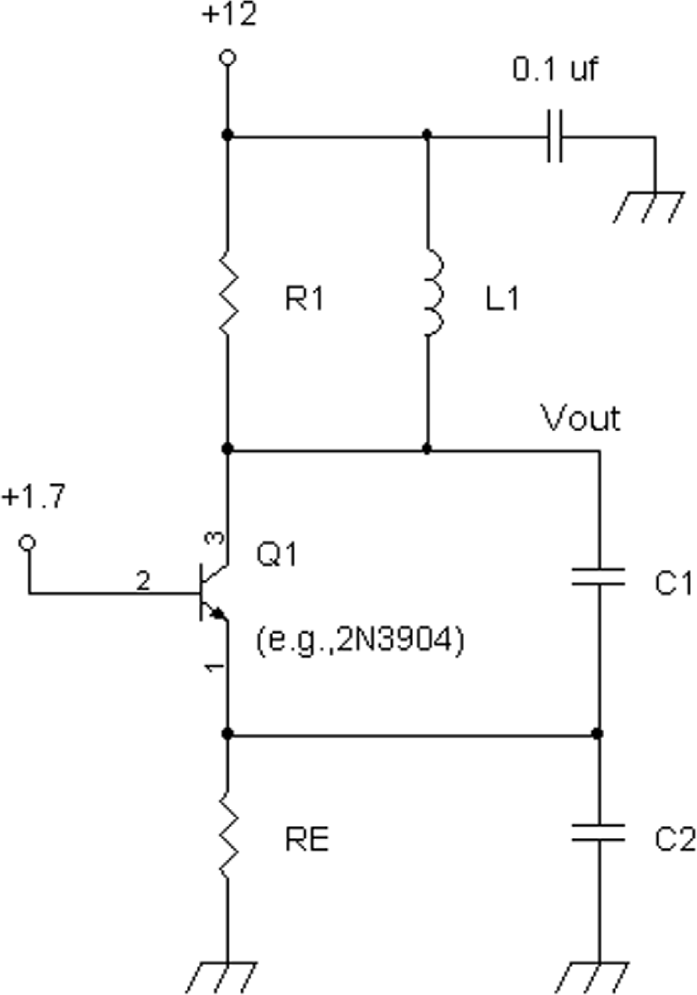
FIGURE 13-9A Colpitts oscillator circuit.
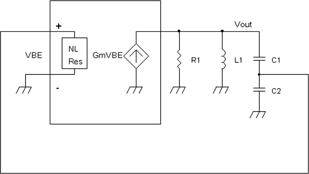
FIGURE 13-9B Alternative diagram for a Colpitts oscillator.
For the values given where R1 = 2,700 ![]() , RE = 1,000 V, C1 = 0.0018 μF, C2 = 0.056 μF, and L1 = 15 μH, the resonant frequency is about 1 MHz, thus providing a 1-MHz signal at the emitter or collector of Q1. With 1.7 volts at the base of Q1, the emitter DC voltage is about 1 volt, which sets up a collector current of 1 mA. The current gain β is greater than 10 (e.g., typically 100 or more). The 1-mA collector current provides a small-signal transconductance gm of 0.038 mho (amperes per volt).
, RE = 1,000 V, C1 = 0.0018 μF, C2 = 0.056 μF, and L1 = 15 μH, the resonant frequency is about 1 MHz, thus providing a 1-MHz signal at the emitter or collector of Q1. With 1.7 volts at the base of Q1, the emitter DC voltage is about 1 volt, which sets up a collector current of 1 mA. The current gain β is greater than 10 (e.g., typically 100 or more). The 1-mA collector current provides a small-signal transconductance gm of 0.038 mho (amperes per volt).
Since at 1 MHz C2’s impedance almost grounds the emitter or Q1, the initial gain of the system is (gmRL)(1/n), where 1/n is the step-down ratio C1/(C1 1 C2) = 1/31 for this example. Therefore, the initial gain of the system Av = 0.038 × 2,700/31 = 3.2. Normally, the initial small-signal gain of this type of oscillator is between 2.2 and 4. A higher initial small-signal gain can be set, but at the expense of generating more distortion with a larger-amplitude output voltage.
From the initial small-signal gain of Av = 3.2, a reasonable prediction can be made as to what the input amplitude will be. It turns out that 1/Av = 1/3.2 = 0.312 is also approximately Gm/gm that is, in other words,
![]()
From Table 13-2, when Gm/gm = 0.304, the input voltage is about 156 mV. So we can expect with Gm/gm = 0.312 that the input signal voltage across C2 will be on the order of about 156 mV.
The output voltage then will be about 156 mV × 0.312 × 0.038 × 2,700 = 5.0 volts peak. Note that 0.312 × 0.038 = Gm, the large-signal transconductance, which is smaller than the small-signal transconductance by a multiplying factor of about 0.312.
The Q of the tank circuit is determined primarily by the load resistor RL = 2,700; that is,
![]()
The actual capacitance is really smaller because C1 is in series with C2. But because C2 >> C1, C1 can be used in the calculation. So the Q of the circuit is about 30 (give or take 10 percent).
In general, the actual output will be smaller than the predicted output voltage value because the inductor has losses and the transistor includes series emitter and base resistors that reduce its transconductance. For example, with the one-transistor oscillator with the values R1 = 2,700 ![]() , RE = 1,000
, RE = 1,000 ![]() , C1 = 0.0018 μF, C2 = 0.056 μF, and L1 = 15 μH, the actual output was smaller by at least 30 percent. That is, instead of the 5.0 volts peak, fewer than 3.5 volts was provided with a standard fixed inductor and a 2N3904 transistor. It turns out that at 1 MHz, the 15-μH inductor is very lossy and thus has a low Q that lowers the output voltage. By maintaining Av = 3.2 by using the same values for R1 = 2,700
, C1 = 0.0018 μF, C2 = 0.056 μF, and L1 = 15 μH, the actual output was smaller by at least 30 percent. That is, instead of the 5.0 volts peak, fewer than 3.5 volts was provided with a standard fixed inductor and a 2N3904 transistor. It turns out that at 1 MHz, the 15-μH inductor is very lossy and thus has a low Q that lowers the output voltage. By maintaining Av = 3.2 by using the same values for R1 = 2,700 ![]() and RE = 1,000
and RE = 1,000 ![]() and raising the frequency to about 3 MHz by dividing the capacitor values by 10 (i.e., C1 = 180 μF and C2 = 0.0056 pF) and replacing the 2N3904 transistor with a 2N4401, the output increased to about 4.25 volts peak, which is within about 15 percent of the calculated 5.0 volts peak.
and raising the frequency to about 3 MHz by dividing the capacitor values by 10 (i.e., C1 = 180 μF and C2 = 0.0056 pF) and replacing the 2N3904 transistor with a 2N4401, the output increased to about 4.25 volts peak, which is within about 15 percent of the calculated 5.0 volts peak.
It should be noted that the input impedance at the emitter of the transistor is often low enough to cause additional signal loss, which thereby lowers the loop gain of the oscillator. This extra lowering of the loop gain results in a lower oscillator output signal. Normally, C2 is made sufficiently large to load into the emitter with minimal signal loss.
Differential Pair Oscillator
Figure 13-10 shows a differential-pair oscillator circuit that is similar to the ones shown in Figures 9-2 and 9-4 of Chapter 9. Essentially, this circuit has the same elements as the one-transistor oscillator circuit with the exception of an extra transistor to “buffer” the signal from the step-down capacitive voltage divider circuit that results in 1/n step-down ratio = C1/(C1 1 C2).
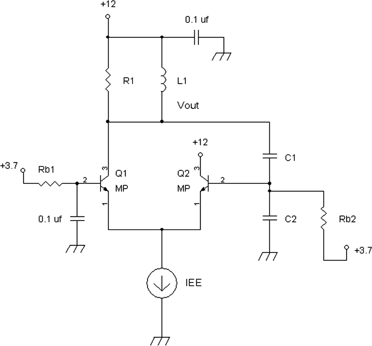
FIGURE 13-10 Differential-pair oscillator circuit.
The advantage of the second transistor Q2 is that the input resistance is at least a factor of β higher than the input resistance to a common-base amplifier, which has an input resistance of 1/gm for small signals or 1/Gm for large signals.
The actual small- and large-signal input resistance at the input of Q2 is = 2β/gm and 2β/Gm, respectively. The reason for the factor of 2 is that the input resistance of Q1 at its emitter acts as a local feedback (degeneration) resistor for Q2. Normally, the input resistance to a common-emitter amplifier is β/gm. Intuitively, the reason for having twice the input resistance is that only half the Vin signal is across the base-emitter junction of Q2, thereby resulting in half the current drain into the base of Q2, which translates into twice the input resistance.
In Figure 13-10, the quiescent currents of Q1 and Q2 are equal; thus the small-signal input resistance at the emitter of Q1 is 1/gm, and the output resistance of emitter follower Q2 is also 1/gm. From Figure 13-11A, Q2 is modeled as a unity-gain amplifier with an output resistance of R_out = 1/gmQ2.
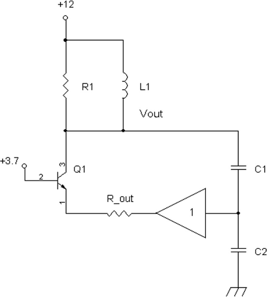
FIGURE 13-11A Differential-pair oscillator with Q2 modeled as a unity-gain amplifier with output resistance R_out.
But the input resistance to the emitter of Q1 is also 1/gmQ1. So the signal voltage at the emitter of Q1 is just one-half Vin, where Vin is the signal from the capacitive divider circuit C1 and C2. Therefore, the small-signal transconductance from Vin at the base of Q2 to the collector output of Q1 is the following:
![]()
where gmQ1 = ICQ1/0.026 volt and ICQ1 is the DC collector current of Q1. Because the current gain β is generally high, the emitter and collector currents of each of the transistors are equal. However, the summed equal emitter or collector currents of Q1 and Q2 equal the emitter tail current IEE, that is,
by various substitutions,

And the small-signal loop gain for the oscillator circuit is
![]()
Usually the small-signal loop gain is set for 2.5 or more to ensure reliable oscillation.
Now let’s take a look at the large-signal characteristics of a differential-pair circuit (Figure 13-11B). The large-signal equation for the collector current of Q1 is as follows for large values of β (e.g., >100):
![]()
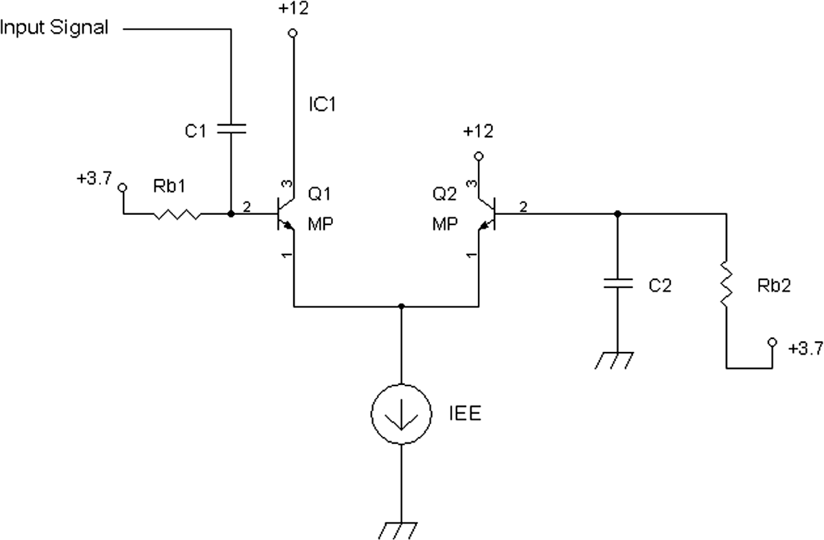
FIGURE 13-11B A differential-pair amplifier that can be used for the oscillator.
With sinusoidal signals of various amplitudes at the base of Q1 in Figure 13-11B, the output current at the collector of Q1 is shown in Figure 13-12. Note in Figure 13-11B that the base of Q2 is grounded AC signal-wise.
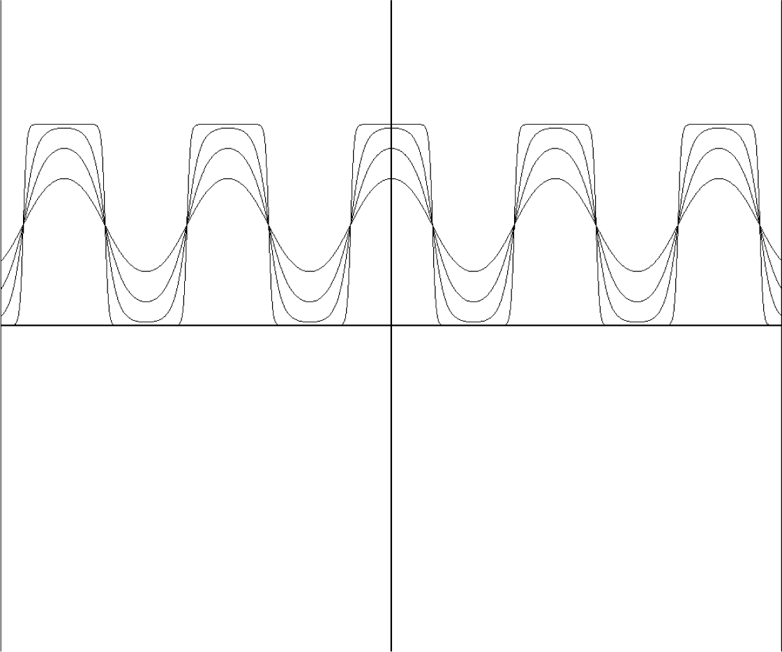
FIGURE 13-12 Q1 collector output current for various amplitude inputs at the base of Q1. The X axis is time, and the Y axis is the output current.
In Figure 13-12, the input levels at the base of Q1 are peak sinusoidal input levels of 26 mV, 52 mV, 104 mV, and 416 mV, respectively. At 26 mV peak, the output current still looks low in distortion, with about 2 percent third-order harmonic distortion. But as the amplitude input level is increased from 52 mV to 416 mV peak, we see that the output current increases in distortion. Distortion is seen at 104 mV, with a soft clipping waveform changing to hard clipping resembling a square wave at 416 mV at the input.
As a result of this distortion, the fundamental frequency signal current at the collector of Q1 will compress as the input signal is increased. So, although the distortion is symmetric compared with the distortion of a single-ended transistor amplifier, as shown in Figure 13-10, there is also a drop in transconductance in a differential-pair transistor amplifier as the input signal is increased.
Table 13-4 shows the approximate* drop-off in large-signal transconductance as a function on input voltage across the bases of the differential amplifier. Note that the large-signal transconductance is output-signal current of the fundamental frequency divided by the input-signal voltage of the fundamental frequency.
TABLE 13-4 Ratio of Large- to Small-Signal Transconductance as a Function of Sinusoidal Input Level

For designing a 3-MHz differential-pair oscillator as seen in Figure 13-10, consider the following: Given that L1 = 15 μH, C1 = 180 pF, C2 = 1,620 pF, and Q = 10, find R1, the emitter tail current IEE and voltage output at the collector of Q1. Note that C1/(C1 1 C2) = 1/10.
The series capacitance of C1 and C2 results in 162 pF. And 162 pF with the 15-μH inductor L results in a resonant frequency of 3.23 MHz. Therefore, Q = 2π(3.23 MHz) RL (162 pF) = 10. Solving for R1 yields R1 = 3,000 ![]() for the closest = percent–valued resistor.
for the closest = percent–valued resistor.
First, pick an initial small-signal loop gain of 3 to solve for the tail current IEE:
![]()
where IEE = 1.04 mA ≈ 1 mA. Because the initial small-signal loop gain = gm/Gm = 3,
![]()
From Table 13-4, this results in about 208 mV across the base of Q2. And because the capacitive voltage divider network C1 and C2 attenuates the collector signal voltage from Q1 by 10, the output voltage at Q1’s collector must be 10 × 208 mV peak, or about a 2-V peak sinusoidal waveform, and thus
![]()
Actually, the output voltage can be calculated via Table 13-4 without directly knowing the tail current IEE when the small-signal loop gain is chosen or established. Since Q2 has a much higher impedance input resistance at the base of Q2 compared to the input resistance at the emitter of the Colpitts oscillator, loading effects from Q2 are ignored because the equivalent large-signal input resistance is 2β/Gm and this large signal resistance is further multiplied by n2 or 100 in this example. Note that 1/n = C1/(C1 1 C2) = (180 pF)/(180 pF 1 1620 pF) = 1/10, or n = 10, and n2 = 100.
Just for “fun,” if β = 100, then the small-signal input resistance is 2β/gmQ1. Then
![]()
where IEE = 1 mA. Thus gmQ1
So 2β/gmQ1 = 10,000 = ![]() small signal–wise. Large signal–wise because gm/Gm = 3,
small signal–wise. Large signal–wise because gm/Gm = 3,
![]()
The equivalent large-signal resistance loading the tank circuit across L1 then is
![]()
which is insignificant to R1 = 3 k![]() in terms of loading the LC tank circuit.
in terms of loading the LC tank circuit.
Unless inductor L1 is a lossless (ideal) inductor, when the oscillator circuit is built based on the equations, a smaller-amplitude oscillation signal will be generated in the range of 10 to 25 percent lower than the calculated amplitude. For example, if the 15-μH L1 inductor is not ideal or lossless and has an unloaded Q of 100, that would be like paralleling a 30-k![]() resistor with R1 = 3,000
resistor with R1 = 3,000 ![]() , which results in a 2,700-
, which results in a 2,700-![]() resistor in parallel with L1. Also, the transistors Q1 and Q2 each have internal base series resistors and internal emitter series resistors that cause a lowering of transconductance from the small-signal equation such as (½) IEE/0.026. A circuit was constructed, and the output voltage was about 1.65 volts peak or low by about 18 percent.
resistor in parallel with L1. Also, the transistors Q1 and Q2 each have internal base series resistors and internal emitter series resistors that cause a lowering of transconductance from the small-signal equation such as (½) IEE/0.026. A circuit was constructed, and the output voltage was about 1.65 volts peak or low by about 18 percent.
References
1. Class notes EE140, Robert G. Meyer, UC Berkeley, Fall 1975.
2. Class notes EE240, Robert G. Meyer, UC Berkeley, Spring 1976.
3. Paul R. Gray and Robert G. Meyer, Analysis and Design of Analog Integrated Circuits. New York: John Wiley & Sons (any edition, e.g., Third Edition 1993)
4. Kenneth K. Clarke and Donald T. Hess, Communication Circuits: Analysis and Design. Reading: Addison-Wesley, 1971.