Chapter 20
Resonant Circuits
Resonant circuits, whether they are constructed from capacitors, inductors, ceramic, or quartz materials, play an important role in passing signals in a particular frequency range and attenuating those signals outside the particular frequency range. Generally, resonant circuits are used in oscillators as well as bandpass filters.
Less commonly known, resonant circuits can be used in all-pass networks to provide group delay equalization or phase equalization to band-pass, high-pass, and low-pass filters. The group delay (GD) can be expressed as GD = Δφ/Δω, where Δφ is the change in phase (in radians), Δω is the change in frequency (in radians per second), and ω = 2πf for a plot of the filter in terms of frequency and phase.
For example, prior to digital finite impulse response (FIR), low-pass filters that provided a square-wave signal with symmetric pre-ringing and post-ringing effects, analog brick-wall filters used in professional (broadcast) video recorders in the 1960s or earlier routinely included a phase equalizer to provide symmetric ringing to pulse waveforms. An all-pass network generally has constant amplitude over a range of frequencies while providing various phase shifts as a function of frequency.
In this book, the radio projects used mainly inductor-capacitor (LC) oscillators and band-pass filters. However, types of resonant circuits such as crystal or ceramic resonator oscillators were shown in Chapters 4 and 12. Ceramic resonators and crystals can be modeled as a series LC circuit with a very large inductor and a very small capacitor, along with a parasitic body capacitance across the two terminal leads of the crystal.
For this chapter, then, the objectives are
1. To examine simple parallel and series LC circuits
2. To understand how resonant circuits play a role in oscillators
3. To show some examples of band-pass and band-reject filters
Simple Parallel and Series Resonant Circuits
Before we start analyzing parallel and series resonant circuits, we need to know the basic characteristics of an inductor and a capacitor. An inductor has the following voltage characteristic with inductance L: Voltage across the inductor L = Vinductor = L(Δi/Δt), where Δi/Δt is the change in inductor current divided by the change in time, and L is the inductance in henries. The current flowing into a capacitor is Icapacitor = C(Δv/Δt), where Δv/Δt is the change in voltage across the capacitor divided by the change in time, and C is the capacitance in farads.
Or, more generally, the voltages and currents of the inductor and capacitor vary with time and can be expressed as functions of time:
![]()
![]()
These basic equations, when applied to differential equations and Laplace/Fourier transforms, result in the complex impedance of the inductor and capacitor when using sinusoidal signals as
![]()
![]()
where j = ![]()
The mysterious j or j operator is defined as the square root of a negative number. Actually, j represents a 90-degree phase shift on a sinusoidal signal. When j is squared, j2 = –1, or think of a sinusoidal signal that has been phase-shifted 90 degrees and another 90 degrees for a total phase shift of 180 degrees. However, 180 degrees of shift on any sinusoidal signal is just an inverted version of the original sinusoid. Hence this is how the –1 term comes in.
Thus jN = N quarter-turns, or N × 90-degree phase shift of a sinusoidal signal. Also, whenever j is used in the context of complex impedances, only sinusoidal or circular functions/signals are used. For complicated signals such as pulses, one can use the j operator with the complicated signals that are equivalently characterized as the summation of sinusoidal signals via Fourier analysis. Then each of the sinusoidal signals can be applied with the j operator.
Figure 20-1 shows a parallel LC circuit that is voltage driven with a resistor. If a direct-current (DC) voltage is applied to an inductor via a resistor, initially the inductor current will be zero. After a period of time, the inductor pulls current and acts like a wire. Thus, in an inductor, applying a voltage across the inductor results in the inductor current having a delay in pulling current. Thus the current in an inductor lags the voltage across the inductor.
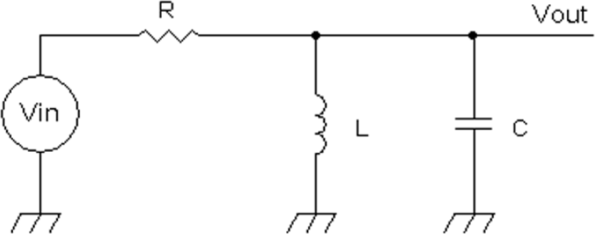
FIGURE 20-1 An LC band-pass filter.
Conversely, if a DC voltage is applied to a capacitor via a resistor, the capacitor will initially act like a short circuit or wire and pull current immediately. After a period of time, though, the capacitor’s voltage starts to match the voltage of the DC voltage source and thereby reduce capacitor current. Thus the current in a capacitor leads the voltage across the capacitor.
When a sinusoidal voltage is applied to an inductor, the inductor current lags by 90 degrees in reference to the inductor voltage. Conversely, a sinusoidal voltage applied to a capacitor results in the capacitor current leading the capacitor voltage by 90 degrees. And when a sinusoidal voltage is applied to an LC parallel circuit where the frequency is chosen such that the magnitude of the impedances of the inductor and capacitor is the same, the inductor current and the capacitor current have the same magnitude, but the currents are a net 180 degrees from each other owing to the inductor’s current having a +90-degree phase shift of the sinusoid voltage and the capacitor’s current having a –190-degree phase shift of the sinusoidal voltage. Because of this 180-degree difference between the inductor and capacitor currents, there is no net current drain looking into the parallel LC circuit at resonance, where
![]()
where Mag = magnitude. The resonant frequency is
![]()
![]()
![]()
![]()
Also note that the impedances of inductors and capacitors have opposite signs.
Thus, with an ideal inductor and capacitor, at resonance, the parallel LC circuit drains no alternating current (AC) and thus has infinite resistance or impedance. For signals that are above the resonant frequency, the impedance drops and looks capacitive because at high frequencies the inductor’s impedance rises, whereas the capacitor’s impedance trends toward a short circuit.
At frequencies below the resonant frequency, the parallel LC circuit starts to look more inductive because the inductor’s impedance drops while the capacitor’s impedance increases. For example, if the signal is DC, the inductor looks like a wire, and the capacitor looks like an open circuit.
In terms of calculating the transfer function of the parallel LC band-pass filter, we will treat the circuit as a voltage divider with the paralleled LC impedance going to ground with the driving resistance R. Thus
![]()
where ![]() and
and
![]()
![]()
After some algebraic manipulations, for the transfer function of Figure 20-1,
![]()
Thus the maximum gain of the transfer function in Equation (20-5) is 1, but in practice, it is less than 1. The reason is that the inductor has resistive and core losses that equivalently connect an extra resistor in parallel with the inductor and capacitor (Figure 20-2).
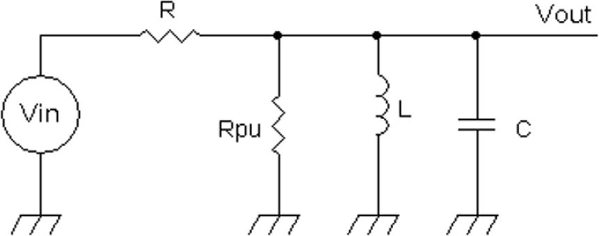
FIGURE 20-2 A parallel LC circuit including the equivalent lossy resistor Rpu.
The resistor R_pu represents equivalent parallel resistance based on the unloaded Q of the coil Qu:
![]()
In general, the Q of the parallel tank circuit is
![]()
And the bandwidth measured from 0.707 of the maximum gain is
![]()
For a current-driven parallel LRC circuit, see Figure 20-3.
Examples of current sources driving an LRC circuit are common-emitter, common-base, and differential-pair amplifiers. The impedance of the LRC circuit is
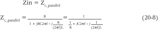
Equation (20-8) states that the maximum impedance when driven with a perfect current source is infinity if the inductor and capacitor have no losses. However, the early effect from the transistor current source and the internal equivalent resistance Rpu will be the limiting resistances across the parallel LC circuit. In terms of the phase relationship with the input signal, at the resonant frequency, the phase shift is 0 degree, and for signals below the resonant frequency, the phase shift is leading or positive up to +90 degrees, whereas for signals above the resonant frequency, the phase shift is lagging and may be as much as –90 degrees. At the frequencies when the signal is 0.707 of the maximum output or –3 dB of bandwidth, the phase shift is +45 degrees at below the resonant frequency and –45 degrees at above the resonant frequency.
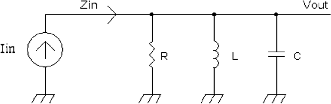
FIGURE 20-3 A current-source-driven LRC circuit.
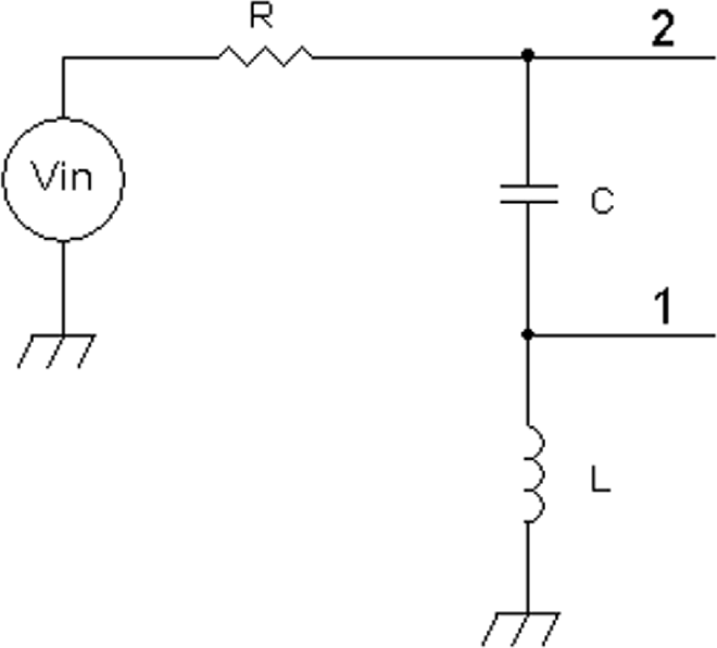
FIGURE 20-4 A series resonant circuit at node 1 as a high-pass filter and at node 2 as band-eject filter.
Figure 20-4 shows a series resonant circuit that can provide different types of filtering. Unlike the parallel resonant circuit, which can be configured for band-pass and band-reject characteristics, a series resonant circuit can be designed for four types of filters: high-pass, low-pass, band-reject, and band-pass filters. For example, the output from node 1 of Figure 20-1 provides a high-pass-filter response. Depending on the driving resistance R, the high-pass filter also can provide a peaked response at the resonant frequency.
Series resonant circuits are also common in ceramic resonators and crystal oscillators, where these types of devices often operate as series resonators. In the parallel resonant circuit, with a voltage source applied across the inductor and capacitor, the currents flowing into the inductor and capacitor are a net 180 degrees from each other. However, in a series resonant circuit with current flowing through the resistor, capacitor, and inductor, the voltage across the inductor and the voltage across the capacitor are a net 180 degrees from each other, and therefore, the net voltage across the capacitor and inductor as seen in node 2 of Figure 20-4 is zero at the resonant frequency.
This zero voltage at the resonant frequency happens because even though there are AC voltages individually across the capacitor and inductor, the “polarity” is out of phase. It is like having two flashlight cells in series connected at either both positive terminals or both negative terminals, which results in the net voltage across the two batteries being zero.
In Figure 20-5, with a voltage source driving the RCL circuit, the current flow is the same through all three devices. The voltage across an inductor leads the current by +90 degrees at resonance, whereas the voltage across a capacitor lags the current by –90 degrees at resonance. Therefore, the net phase difference voltage-wise across the inductor and capacitor is 180 degrees. If the current were in phase, such as a voltage source driving two series resistors, the voltages across each resistor would add up. However, when the phase is opposite, as in the case of the series RLC circuit at the resonant frequency, equal and opposite AC signals are occurring, and a cancellation effect results when the voltage is taken at Vout where the inductor and capacitor are in series.
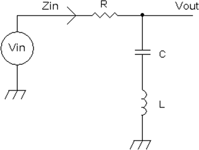
FIGURE 20-5 Series resonant circuit where at resonance the voltage drops to zero across the series capacitor-inductor circuit.
The impedance of the series RLC circuit is Zin = ZLC_series’, which is
![]()
The Q of a series RLC circuit is
![]()
where QS_LL is the Q for a lossless inductor L.
However, as stated previously, an inductor includes losses, and in a series resonant circuit, the coil has an internal resistance based on coil resistance and core losses as Rser. For Equations (20-9) and (20-10), Rser = 0.
Generally, for low- or high-pass filters in series resonant circuits, the Q requirement is very low, <1 (e.g., 0.6 to 1). Therefore, Rser is not as important in the overall frequency response of high- passor low-pass filters compared with band-pass or notch filters, where the Q typically is greater than 10.
For a band-pass series RLC circuit, the voltage source is driven as shown in Figure 20-6 with Rser. With the resistor as the output terminal, the transfer characteristic for the series resonant band-pass filter is
![]()
and
![]()
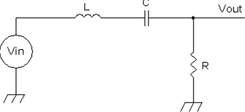
FIGURE 20-6 A series LC band-pass filter.
R_ser is the equivalent internal series lossy resistor of the inductor.
The frequency response of either parallel or series resonant band-pass filters can be characterized as a function of Qp or Qs. The –3-dB bandwidth is
![]()
where Q is either Qp or Qs depending on whether a parallel or series resonant circuit is being used.
To find the relationship between the amplitude at the center frequency, which is the resonant frequency fres, and the amplitude of signals whose frequencies are below or above fres by Δf, see Equation (20-13):
For example, suppose that the center frequency fres = 1,000 kHz and the Q is 50, then
![]()
Then
![]()
If Δf = 10 kHz, then the attenuation factor is 0.707 at 1,010 kHz and 990 kHz. If Δf = 100 kHz, then the attenuation factor is 0.10 at 1,100 kHz and 900 kHz. When
![]()
the attenuation factor from the center frequency is characterized as ≈
In a series resonant circuit, at resonance, the impedances of the inductor and capacitor cancel, and thus the series impedance of the capacitor and inductor is zero. This means that if the driving resistance is very low, very large amounts of AC current can flow through the capacitor and inductor. What is also important to observe is that at resonance, the AC voltage across the inductor or capacitor can exceed the input signal. In a sense, there is a step-up voltage effect when using the series resonant circuit in a particular manner.
For example, at node 1, the AC voltage across the inductor is determined by the AC current flowing through it. At resonance, this AC current is just
![]()
However, the magnitude of the AC voltage across the inductor L is the inductor current multiplied by the magnitude of the impedance of the inductor, as seen in Equation (20-15):
![]()
For example, if Qs = 10, by setting R to a low resistance value, the AC voltage across the inductor will be 10 times the AC voltage of the input signal generator. In a sense, the series RLC circuit can be thought of as a step-up transformer. One should note, however, that although the voltage across the inductor is larger than the input signal, the phase of the inductor voltage leads the phase of the input by +90 degrees at resonance, where ![]() . This positive phase shift at the inductor makes sense because the voltage across the inductor forms a high-pass filter, which provides a positive or leading-phase relationship when compared with the input signal.
. This positive phase shift at the inductor makes sense because the voltage across the inductor forms a high-pass filter, which provides a positive or leading-phase relationship when compared with the input signal.
It should be noted that the impedance of the series RLC circuit is more capacitive below the resonant frequency (because at DC the inductor is like a wire), resistive at the resonant frequency with resistance R, and inductive (because at high frequencies the capacitor is like a short circuit) at above the resonant frequency.
The high-pass filtering characteristic of the series RLC circuit with voltage “gain” or step-up capability along with the positive phase shift is serendipitous for providing oscillations with an amplifier whose voltage gain is less than 1. If the series RLC circuit is configured as a low-pass filter, as seen in Figure 20-7, a voltage gain or step-up capability can be achieved along with a negative phase shift.
At resonance, the phase shift is –90 degrees. Also, depending on the driving resistance R, the “gain” can be greater than 1 at the resonant frequency, similar to how Q affects the “gain” in the high-pass filter circuit. To reiterate, see Equation (20-12) on the Q of a series resonant circuit:
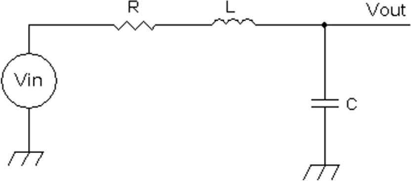
FIGURE 20-7 Series resonant circuit configured for a low-pass filter effect.
![]()
Oscillators that use an inverter gate and capacitors at the output and input along with an inductor or crystal or ceramic resonator between the output and input use a series resonant low-pass filter for oscillation.
Resonant Circuits in Oscillators
This section will examine three types of oscillators that use series resonant circuits. Figure 20-8 shows a series resonant oscillator with a unity-gain amplifier. In the figure, although the amplifier has a voltage gain of 1 or less than 1, it has the capability to provide current, which will be used to step up AC signal voltages. The output of the unity-gain amplifier is low-pass-filtered with an RC filter, which provides a phase lag or negative phase shift. A series high-pass filter circuit consisting of capacitor C and inductor L is connected to the output of the low-pass filter at C1. The inductor of the high-pass filter is connected to an AC ground, which when driven by the low-pass filter output at C1 provides an increase in signal voltage and positive phase shift to cancel the negative phase shift of the low-pass filter. The cancellation in phase shifts provides a zero net phase shift of signals between the input and output of the unity-gain amplifier. And the unity-gain amplifier has current gain and is able to drive the high-pass filter C and L sufficiently to step up the signal voltage such that there is an equivalent voltage gain at the input of the unity-gain amplifier. Thus oscillation occurs at or near the resonant frequency ![]()
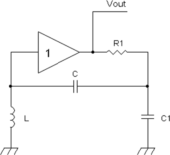
FIGURE 20-8 A series resonant oscillator.
Figure 20-9 shows a practical implementation of Figure 20-8 using a transistor. Emitter follower Q1 is biased to a base voltage of Vbias by connection of the inductor L. With a 0.6 volt-base emitter voltage drop, the collector current of Q1 is
![]()
Because the base is driven via an AC voltage across an inductor and not a pure voltage source, the actual output resistance is higher than the approximation of the output resistance of Q1 at the emitter of
![]()
where ![]()
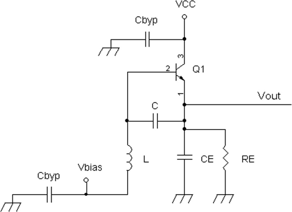
FIGURE 20-9 An emitter follower oscillator using a series resonant circuit.
The capacitor CE forms a low-pass filter with Rout at the emitter with a cutoff frequency of about
![]()
For example, let RE = 12 k![]() , Vbias = 1.8 volts DC, L = 220 μH, C = 220 pF, and CE = 1,800 pF. Then
, Vbias = 1.8 volts DC, L = 220 μH, C = 220 pF, and CE = 1,800 pF. Then
For a starting point, capacitor CE is chosen to a value such that fcutoff is about the resonant frequency or a little below the resonant frequency:
which is the approximate frequency of oscillation.
The measured frequency of oscillation is 769 kHz, but remember that although CE >> C, capacitor CE can contribute to the oscillation frequency because it is in series with capacitor C. Let’s calculate the series capacitance of CE and C, and use that value to recalculate the resonant frequency. The series capacitance of CE and C is
which is closer to the measured frequency of 769 kHz.
One question is, could the value of CE be increased further? The answer is yes and no. Yes, as long as there is a reliable oscillation. No, because there will be a point where CE is too large in capacitance, and the gain loss from the roll-off in response will stop the oscillation. For example, if CE were changed from 1,800 pF to 18,000 pF, there would be about a 10-fold loss in gain, and if the Q of the LC circuit is not high enough, there will be insufficient gain to sustain an oscillation. Recall that a gain of at least 1 is needed with a net phase shift of 0 degree.
The oscillator circuit shown in Figure 20-10 also can explain why at times some common-emitter amplifiers or some emitter follower circuits self-oscillate. Common-emitter amplifiers without the emitter AC grounded or emitter follower circuits generally load into some small capacitance C_load at the emitter to cause a phase lag at high frequencies. All transistors have an internal base emitter capacitance Cπ = Cpi, which, although small, still serves as a capacitor from the emitter back to the base. The base lead or wires connected to the base include a parasitic or stray inductance, which then resonates with Cπ or Cpi. Usually, the self-oscillation frequency is at 100 MHz or higher, and placing a series resistor of 47 ![]() to 470
to 470 ![]() very near to the base reduces the Q of the parasitic/stray inductance by adding resistance to the stray inductor. Therefore, the added base resistor reduces the voltage-gain effect of a series resonant circuit that stops the oscillation. Recall that the Q for a series resonant
very near to the base reduces the Q of the parasitic/stray inductance by adding resistance to the stray inductor. Therefore, the added base resistor reduces the voltage-gain effect of a series resonant circuit that stops the oscillation. Recall that the Q for a series resonant
circuit is
![]()
Figure 20-10 shows a base oscillation-stopping resistor, R_base stop, for an emitter follower circuit.
Another oscillator circuit that uses series resonant circuits is a crystal oscillator, as shown in Figure 20-11. Figure 20-12 shows an equivalent LC oscillator circuit to that in Figure 20-11. In Figure 20-12, the crystal is modeled as a series resonant circuit with an inductor Lcrystal and a capacitor Ccrystal. Typically, the value of Ccrystal is in femtofarads or on the order of less than 0.1 pF, and inductor Lcrystal has the equivalent inductance in millihenrys.

FIGURE 20-10 Emitter follower circuit with a base-stopping resistor to avoid oscillation.
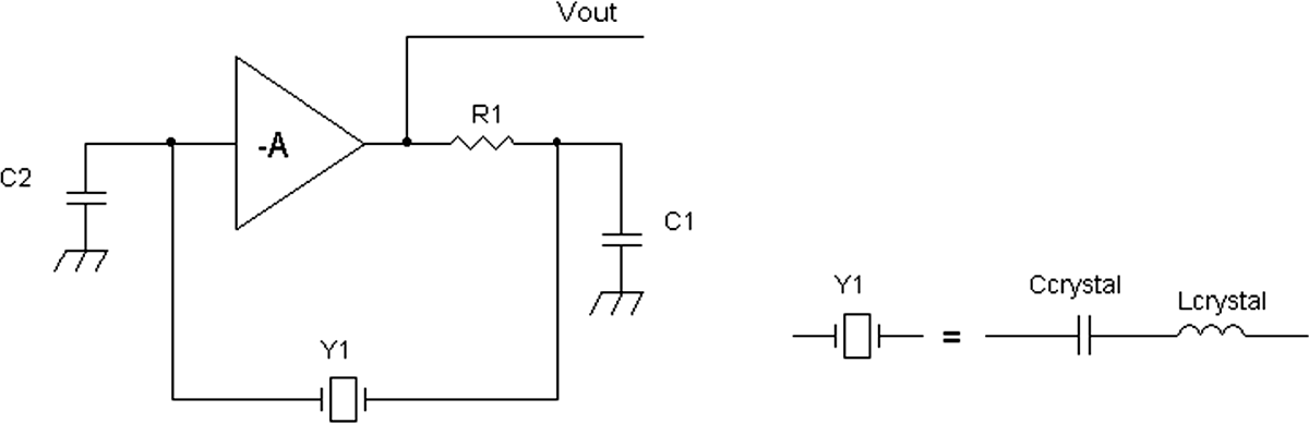
FIGURE 20-11 A crystal oscillator using an inverting amplifier.
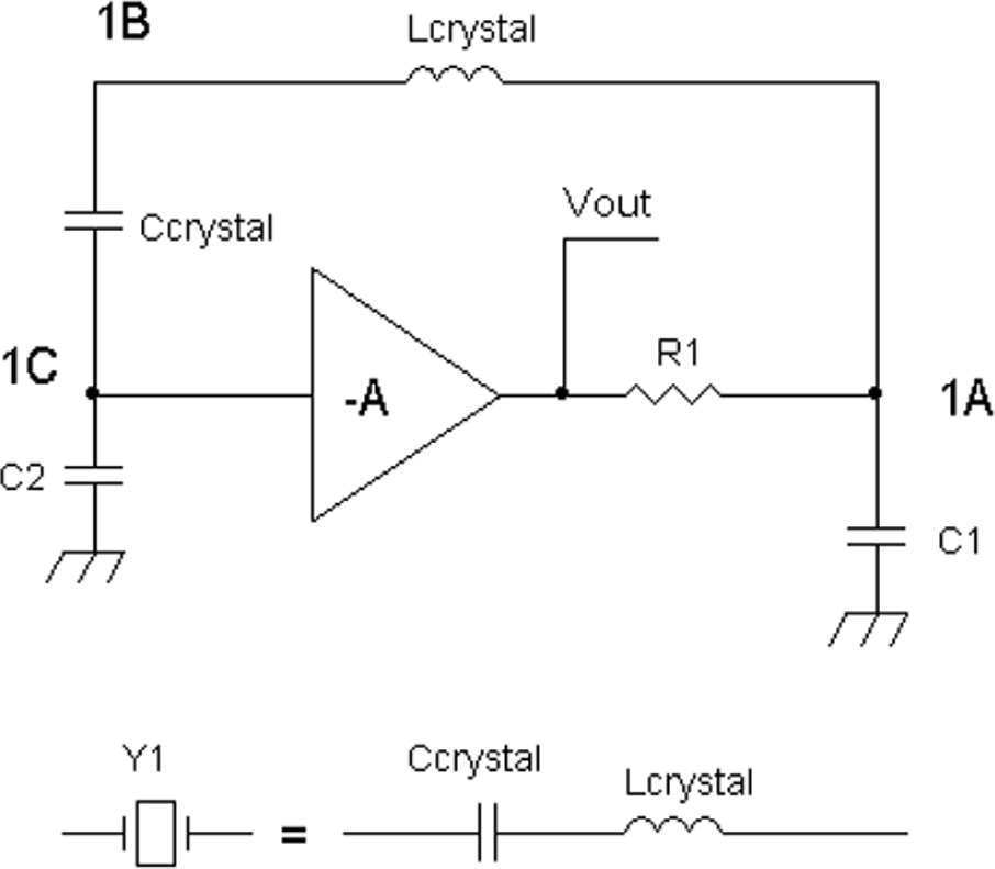
FIGURE 20-12 An equivalent circuit to Figure 20-11 with an inductor and capacitor to model the crystal.
Figure 20-13 shows series and parallel modes for crystals. In Figure 20-13, basically, the difference between series and parallel modes is just that the parallel-mode crystal is cut such that when the crystal is in series with a loading capacitor C_load, with a value such as 18 pF, the crystal will oscillate at the given frequency. A series-mode crystal will operate at its given frequency without a series capacitor. Either parallel or series mode can oscillate with other values of series capacitors to “pull” the crystal frequency on order of about 0.15 percent.
A 28.636-MHz crystal rated at 18 pF loading provided a frequency of 28.636 MHz, with C_load being an 18-pF loading capacitor. However, with C_load equal to 100 pF, the oscillator provided a frequency of 28.600 MHz. From these two measurements, the internal capacitance of Ccrystal was calculated to be about 0.063 pF.
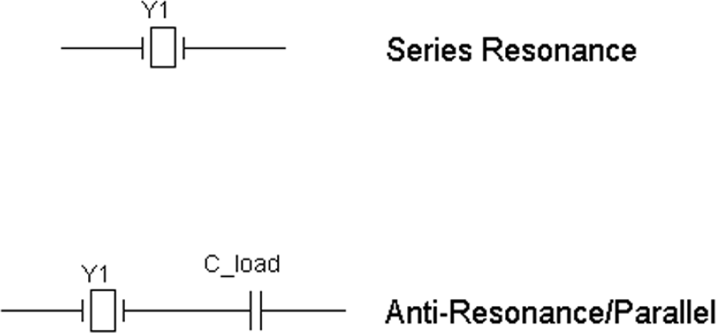
FIGURE 20-13 Series crystal and parallel/antiresonant crystal modes.
In Figure 20-12, the capacitors Ccrystal and C2 provide a capacitive voltage divider from node 1B. A capacitive voltage divider keeps the same phase of the signal from nodes 1B and 1C. However, the signal at node 1C is an attenuated version of the signal at node 1B.
The inverting amplifier’s output is connected to a low-pass filter R1 and C1 to provide a lagging phase shift because the phase shift from R1 and C1, plus the phase shift from Lcrystal and Ccrystal must provide 180 degrees of phase shift. Typically, the phase shift from R1 and C1 lags about 60 degrees to 80 degrees, and the phase shift from Lcrystal and Ccrystal can be in the range of 100 degrees to 135 degrees lagging. Thus the combination of R1 and C1 and the crystal provides the required phase shift for oscillation.
Although the attenuation from the capacitive voltage divider is around 100 or more, the gain of the inverting amplifier and the extremely high Q of the crystal (e.g., Q > 1,000) provide sufficient overall gain to overcome the attenuation from the capacitive voltage divider (Ccrystal and C2) to provide a reliable oscillation.
Figure 20-14 presents examples of crystal and ceramic resonator oscillators based on Figures 20-11 and 20-12. Although the Figure 20-14 shows using CMOS gates for the inverting amplifiers, other implementations include using a single-transistor or field-effect-transistor (FET) common-emitter or common-source amplifier instead.
For example, the FET amplifier will have a drain load resistor and a capacitor (e.g., 18 pF to 47 pF) from the drain to ground. The crystal is connected between the drain and the gate of the FET. At the gate, there is a high-resistance biasing resistor (e.g., >500 k![]() ) and another capacitor (e.g., 18 pF to 47 pF) from the gate to ground. This type of oscillator is often referred to as a Pierce oscillator.
) and another capacitor (e.g., 18 pF to 47 pF) from the gate to ground. This type of oscillator is often referred to as a Pierce oscillator.
FIGURE 20-14 Crystal and ceramic resonator oscillators U1C and U1A.
We now turn our attention to another type of series resonant crystal oscillator, the two-gate oscillator (Figure 20-15). With a two-gate oscillator as shown in Figure 20-15, at series resonance, the impedance of the crystal drops sufficiently to ensure positive feedback. The advantage of this type of crystal oscillator circuit is that the frequency of the parallel mode (otherwise known as an antiresonant mode) allows dropping the crystal frequency by at least 0.15 percent. For example, if the series capacitor C_load’ is set to the loading capacitance of about 18 pF, the oscillator will provide a frequency as shown on the parallel-mode crystal. However, if the frequency needs to be lowered, then a larger series capacitance via C_load’, such as 56 pF to 1,000 pF, can be used to lower the oscillator’s frequency.
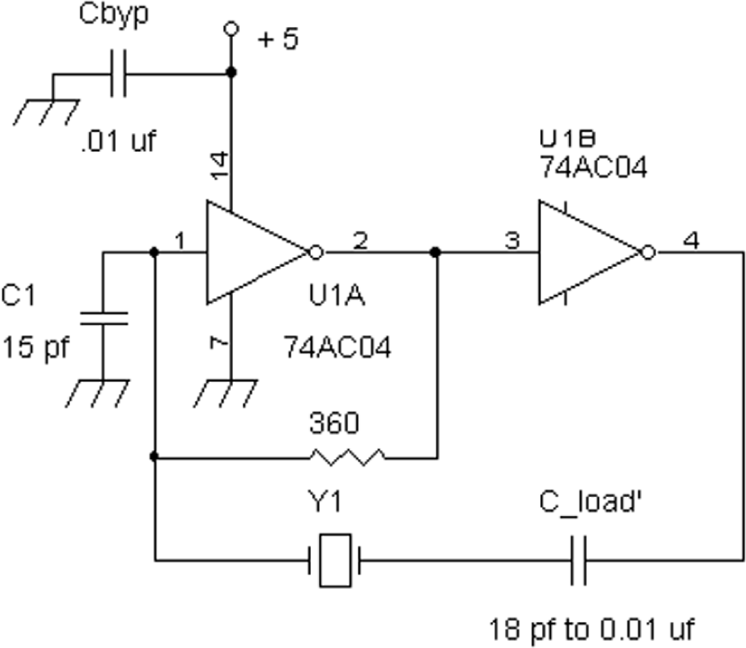
FIGURE 20-15 A two-gate crystal oscillator for series resonant mode.
Likewise, if a series crystal is used, normally the series capacitor C_load’ is an AC short circuit, such as a 0.01-μF capacitor. However, if the frequency needs to be raised by as much as 0.15 percent, a series capacitor with a value as low as 18 pF can be used.
In practical terms, as mentioned previously, a standard parallel-mode 28.636-MHz crystal with 18-pF loading can be used for the 40-meter amateur radio band simply by installing it in the oscillator circuit of Figure 20-6 with the series capacitor C_s with a value of about 100 pF instead of the 18-pF capacitor. With the 100-pF series capacitor, the oscillation frequency will be pulled down to 28.600 MHz (a 36-kHz downward shift). Afterwards, just divide the frequency of the 28.6000-MHz signal by 4 to provide 7.150 MHz.
Examples of Band-Pass and Band-Reject Filters
At times, a simple band-pass filter may not provide sufficient selectivity in a radio. A way to increase selectivity is by cascading or linking band-pass filters. Figure 20-16 shows two parallel LC circuits linked together with a capacitor.
The parallel circuit L1 and C1 is driven with resistor R via a voltage source Vin. From the output of the first section, a coupling capacitor C3 links the signal from L1 and C1 to another parallel tank circuit C2 and L2. In many instances, L1 = L2, C1 = C2, and C3 = 0.5 to 3 percent of C1. For example, if C1 = 500 pF, C3 = 15 pF (3 percent of 500 pF). Driving resistor R can be chosen for a Q of 15 to 20 for a starting point depending on the bandwidth desired. There are many variations of this circuit, such as a variable capacitor for C1 or C2, a variable inductor for L1 or L2, or a loading resistor across L2 to shape the bandwidth. The output at L2/C2 should be coupled to a high-resistance amplifier to maintain the Q of the L2/C2 tank circuit and make up for signal losses.
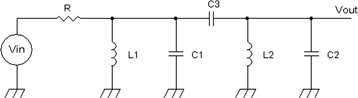
FIGURE 20-16 A two-stage band-pass filter.
Figure 20-17 shows examples of band-reject filters, one with a parallel LC circuit and another with a series LC circuit. Notch or band-reject filters pertaining to standard amplitude-modulation (AM) radios are not used commonly. In frequency-modulated (FM) radios, a notch filter such as a 10.7-MHz series resonant filter is placed at the input of the mixer or the output of the radio-frequency (RF) amplifier to ensure that the mixer output has a 10.7-MHz intermediate-frequency (IF) signal from the result of mixing RF signals from 88 MHz to 108 MHz with the FM radio’s local oscillator’s signal.
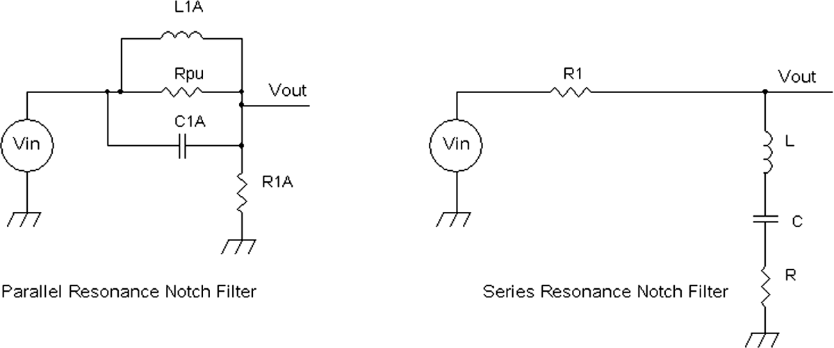
FIGURE 20-17 A parallel resonant notch filter and a series resonant notch or band-reject filter.
Recall that the impedance of a parallel LC network is
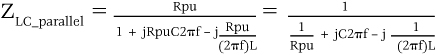
where Rpu in this case is the equivalent lossy parallel resistance owing to coil resistance and core losses.
For a parallel resonant notch filter,
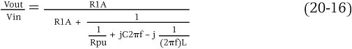
At resonance, the parallel LCR circuit has the L and the C impedances canceling out, thus leaving only the resistance Rpu. So
![]()
Therefore, it is advantageous to have Rpu as high a resistance as possible for maximum attenuation at the resonant frequency:
![]()
If there are no losses in the inductor L, Rpu = infinity = ∞, and
which means for any given R1A, at resonance, the notch or drop in signal voltage at the output is zero. However, this is not the case in practice. Typical starting values for R1A can be in the range of a few hundred ohms to 1,000 ![]() .
.
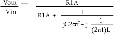
For the series LC notch circuit in Figure 20-17,
At resonance, the impedance of the series combination of L and C is zero, leaving
![]()
where R is the equivalent series lossy resistance owing to coil resistance and core losses. Thus it will be advantageous to obtain a coil or inductor with the lowest equivalent R.
And, of course, for a perfect inductor where R = 0, at resonance, and R1 > 0,
![]()
For choosing R1, the driving resistance for a series resonant notch filter, a resistor in the range of 1,000 ![]() to 10,000
to 10,000 ![]() is a good starting point. One should keep in mind that the series resonant capacitor C also forms a one-pole low-pass filter with R1 if the inductor L has a low inductance. So, once the resonant frequency fres is known and the value of R1 is chosen, generally try to choose C in such a way that the low-pass filter cutoff frequency is at or higher than the resonating frequency. That is,
is a good starting point. One should keep in mind that the series resonant capacitor C also forms a one-pole low-pass filter with R1 if the inductor L has a low inductance. So, once the resonant frequency fres is known and the value of R1 is chosen, generally try to choose C in such a way that the low-pass filter cutoff frequency is at or higher than the resonating frequency. That is,
![]()
Once the value of C is chosen, then the inductance of L can be calculated. This recommendation is to avoid having the roll-off of the notch filter occur prematurely, before the “notch” effect comes in. It is better to have a relatively flat frequency response until very close to the notch frequency and then let the series resonant effect take over and cause a steep dip in amplitude.
Figure 20-18 shows combination band-pass and band-eject (notch) filter. During the earlier days when there were very few radio stations in an area, superheterodyne receiver designs had a very low IF, on the order of 100 kHz or less. The image-frequency problem, where another station at twice the IF above the tuned desired station could mix back into the IF band, was not common as long as the stations’ frequencies were separated far enough from each other. However, later on, more and more radio stations were crowding the AM band, and the image-frequency problem became very real. Before the 455-kHz IF was used as the standard IF, the earlier radios used a much lower IF band. And in order to address the image-frequency problem during those early days of radio, a front-end radio circuit consisted of two types of variable-frequency filters. One was a band-pass filter to tune to the desired frequency, and another was a notch or band-reject filter that resonates at a frequency above the desired frequency with a separation of twice the IF.
For example, suppose that the IF is 100 kHz. If a desired station is tuned to 600 kHz for the band-pass filter, the notch filter is tuned to 2 × 100 kHz above 600 kHz, or at 800 kHz, for a band-reject (notch) filter. In this way, the image-frequency signal at 800 kHz would be attenuated or removed.
Figure 20-18 shows a band-pass filter consisting of the secondary winding of an RF transformer T1 that resonates with the variable capacitor VC1A that tunes to the desired frequency. The output signal from VC1A then is coupled with a very small capacitance Co (e.g., < 6 pF) to inductor L, which is an inductor that has less inductance than the secondary winding of T1. VC1A and VC1B form a twin-gang variable capacitor. Variable capacitor VC1B then resonates with inductor L to notch-out or band-reject frequencies related to the image-frequency signal. The output then is coupled to another RF amplifier stage or to a mixer.

FIGURE 20-18 A combination band-pass and band-eject filter using capacitive coupling.
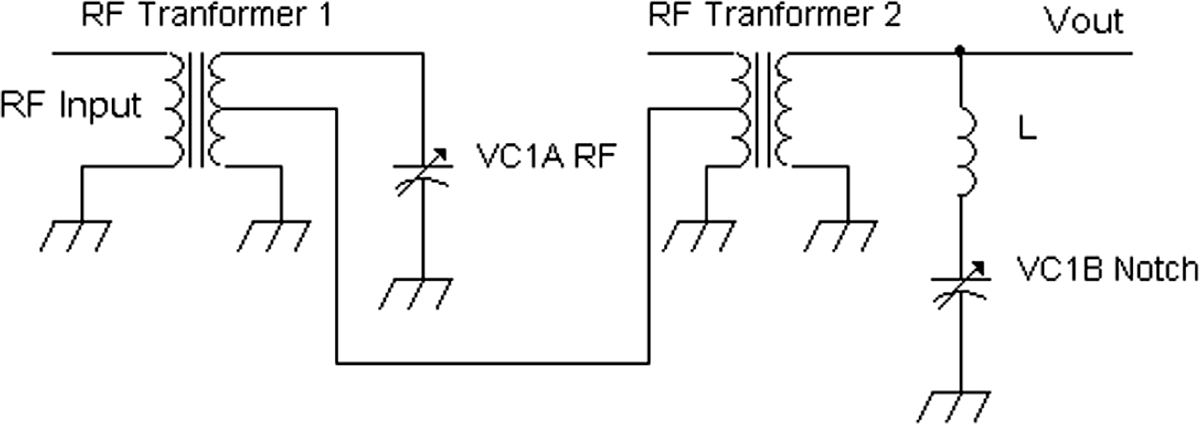
FIGURE 20-19 A combination band-pass and band-reject filter for image signal rejection.
Figure 20-19 shows a transformer-coupled circuit that reduces the image-frequency signal that is similar to the Atwater Kent superheterodyne radio Models 70, 72, 74, and 76, which were made in the early or middle 1930s.
RF Transformer 1’s secondary winding resonates with variable capacitor VC1A for tuning into the desired radio station frequency. A low-impedance tap from the secondary winding of RF Transformer 1 is coupled to a low-impedance winding of RF Transformer 2. The secondary winding of RF Transformer 2 is stepped up, which provides a higher impedance than its primary winding. The secondary winding of RF Transformer 2 then is connected to a series resonant circuit consisting of inductor L and variable capacitor VC1B. Preferably, VC1A and VC1B are identical. The inductor L generally has less inductance than the inductance of RF Transformer 1’s secondary winding to provide a notch or band-reject characteristic at a higher frequency than the tuned RF signal.
For example, the notch or band-reject frequency is tuned RF frequency + 2 × IF, or
![]()
In the Atwater Kent Radio Model 70, IF = 130 kHz; thus the band-reject filter is tuned to the (tuned RF frequency + 2 × 130 kHz) = (tuned RF frequency + 260 kHz), or 260 kHz above the tuned RF frequency.
References
1. Arthur B. Williams and Fred J. Taylor, Electronic Filter Design Handbook, 2nd ed. New York: McGraw-Hill, 1988.
2. Class Notes EE140, Robert G. Meyer, UC Berkeley, Fall 1975.
3. Class Notes EE240, Robert G. Meyer, UC Berkeley, Spring 1976.
4. Paul R. Gray and Robert G. Meyer, Analysis and Design of Analog Integrated Circuits, 3rd ed. New York: John Wiley & Sons, 1993.
5. Kenneth K. Clarke and Donald T. Hess, Communication Circuits: Analysis and Design. Reading: Addison-Wesley, 1971.
6. Robert L. Shrader, Electronic Communication, 6th ed. New York: Glencoe/McGraw-Hill, 1991.
7. William G. Oldham and Steven E. Schwarz, An Introduction to Electronics. New York: Holt Reinhart Winston, 1972.
8. Allan R. Hambley, Electrical Engineering Principles and Applications, 2nd ed. Upper Saddle River: Prentice Hall, 2002.
9. Gene F. Franklin, J. David Powell, and Abbas Emami-Naeini, Feedback Control of Dynamic Systems, 3rd ed. Reading: Addison-Wesley, 1995.
10. Howard W. Sams & Co., Sams Photofact Transistor Radio Series, TSM-100. Indianapolis, May, 1969.
11. John F. Rider, Servicing Superheterodynes. New York: John F. Rider, 1934.
12. Lap-Tech Precision, Inc., Quartz Products by Lap-Tech. Bowmanville, Ontario, Canada: 1990.