Chapter 12
Introduction to Software-Defined Radios (SDRs)
Chapter 11 presented a different type of superheterodyne radio—a coil-less receiver. Two new concepts were introduced—image signals and switching-type radio-frequency (RF) signal mixers. It was also in Chapter 11 that image signals were shown to be eliminated or attenuated by providing a band-pass filter prior to RF mixer so that the desired signal is output from the mixer and not the image signal. In the coil-less radio, a higher intermediate frequency (IF) of 600 kHz was used with a 1.6-MHz low-pass filter to provide image signal rejection. The coil-less radio is rather simple to implement with integrated circuits.
It should be noted that in Chapters 8 through 11, the selectivity of the superheterodyne radio was influenced by the band-pass characteristics of the IF filter. If more selectivity is required, then usually more IF transformers, coils, and/or ceramic filters must be added to the design. And if the IF needs to be changed to some frequency other than 455 kHz, then the IF transformers or ceramic filters need to be replaced.
So one of the main motivations for a using a computer or digital processing in superheterodyne radios is to replace the IF section, whereby the IF filters can be generated in the digital domain. Once an analog signal is digitized by an analog-to-digital converter, the digital domain can take over to mimic many of the past analog functions, such as filtering, RF mixing, delaying signals, or amplifying the IF signals. In the digital domain, the frequency and band-pass characteristic (e.g., bandwidth) can be designed with flexibility. For example, with digital filtering, the band-pass filter characteristics can be tailored to any specific bandwidth without changing the hardware.
So, if one needs a 455-kHz filter in the digital domain to have narrower or broader bandwidth, just setting some registers in the digital filter program changes the filter characteristics. So there is no need to change a physical part. The filter’s characteristic is determined by software.
And as technology progresses, more and more circuits can be mimicked in a computer or in a system on a chip via digital signal processing to provide not only filtering but also amplification, tuning across the IF band (e.g., 44.1 kHz to 192 kHz), phase shifting, multiplication (e.g., RF mixing) that includes image-reject mixing, and detecting [amplitude-modulated (AM) and frequency-modulated (FM) demodulators] via software.
One popular implementation of a software-defined radio (SDR) on a chip is a two-band 2-m and 70-cm transceiver made by Baofeng. This radio sells for about $40 and uses a dedicated SDR integrated circuit, the RDA 1846. Because this radio does not have too much RF filtering in the front end, it is susceptible to overload when used near a transmitter (e.g., amateur radio FM repeater). But otherwise it performs very well.
Another popular implementation of the SDR is via several do-it-yourself software-defined radio programs that run on a computer, such as the Winrad program. There are other SDR programs that will run on PCs. For example, once the Winrad program is installed on a PC (e.g., XP or Windows 7 operating system), all that is needed is a down-converted low-frequency IF signal to be provided to the audio inputs of the computer’s sound card. The PC then takes over the IF filtering, tuning, and demodulation. Because the low-frequency IF signal has a wide bandwidth of at least half the sampling frequency of the sound card, radio stations can be tuned via the Winrad software program over a 201-kHz range. Thus the Winrad program also provides the equivalent of a variable-frequency oscillator.
For many SDRs, switch-mode mixers will be used, and image rejection will be handled in the software via digital signal processing. So now let’s look at two examples of SDR front-end systems. They both provide two channels of down-converted low-frequency IF signals to the two input channels of a computer’s sound card.
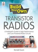
Figure 12-1A provides a first example of an SDR front-end block diagram. An antenna is connected to generally a fixed-frequency RF band-pass filter, but a tunable filter can be used. This RF band-pass filter will be needed to remove signals whose frequencies are outside the band of interest so that out-of-band signals do not mix back down to the IF band. For example, in the 40-m amateur radio band, signals around 7.2 MHz should be passed through, but frequencies above 8 MHz should be attenuated. The RF band-pass filter in an SDR system generally is not used to remove image signals but to remove out-of-band signals because the mixer that is used is a harmonic mixer.
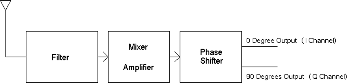
FIGURE 12-1A First example of an SDR front-end system using analog phase shifters.
Briefly, almost every RF mixer is a harmonic mixer of some sort. So what is meant by harmonic mixing? A harmonic mixer is capable of providing a signal that falls into the IF band by way of out-of-band RF signals producing a difference signal with a harmonic of the local oscillator’s frequency.
Let’s take an example of a theoretical broadcast AM radio system in which there is no tuned RF filter prior to mixing. Recall from Chapter 8 that superheterodyne radios always use a tuned RF filter via variable capacitor VC1_RF to pass the radio station’s signal to the mixer or converter circuit. And recall that the local oscillators or converter circuits in Chapter 8 have large oscillator signals that purposely cause distortion in order to provide a multiplying effect in the mixer or converter circuits. This distortion owing to the large amplitude of the oscillator signal also results in harmonics of the local oscillator frequency. Table 12-1 provides an example with a 455-kHz IF system (note that LO = local oscillator).
TABLE 12-1 Out-of-Band Radio-Frequencies Mixing Undesirably to the 455 kHz IF from Harmonics of the LO (Local Oscillator) Signal
As can be seen from the table, without any filtering prior to RF mixing, unwanted signals of frequencies from 1.52 MHz to 5.84 MHz will mix into the 455-kHz IF band and thus cause the radio to receive extraneous signals. Note that noise from 1.52 MHz to 5.84 MHz also will mix into the IF band, resulting in extra or increased noise levels when the 455-kHz IF signal is demodulated.
So in Figure 12-1A a filter is used to ensure that out-of-band noise and signals are not down-converted to the IF band. The output of the mixer then is connected to a constant-amplitude phase-shift circuit that provides two outputs. Relative to one of the outputs of the phase-shifter network is a constant 90-degree shift over a range of frequencies. A first output of the phase-shifter circuit is normally defined as the I channel, or in-phase channel, whereas the second output that has the constant 90-degree phase shift relative to the first output is named the Q channel, or quadrature channel.
A computer’s sound card then captures the signals from the I and Q channels of the phase-shifter circuit, which contain signals of a low IF (e.g., 3 kHz to 96 kHz). Now the question is, Why connect two types of signals to the sound card?
As stated earlier, the RF filter in Figure 12-1A does not filter out image signals. So there must be some other way to remove image signals. By using I and Q signals and connecting them to an image-signal-reject mixer circuit that is emulated by digital signal processing in the computer, image signals are attenuated. It will be shown in much more detail in Chapter 21 that signals that are 90 degrees relative to each other can be used to cancel out image signals while passing the desired signals, or vice versa, that is, passing image signals while canceling out the desired signals.
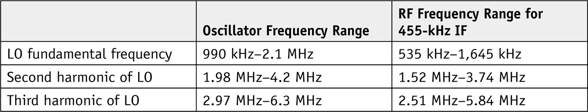
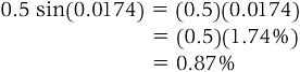
Figure 12-1B shows a more common way of generating I and Q signals at low IFs for coupling into the computer. The analog phase-shift network is replaced by an I and Q mixer system, which consists of two mixers. So in Figure 12-1A there is one mixer and an analog phase-shift network. And in Figure 12-1B there are two mixers instead to provide the phase-shifting function that replaces an analog phase-shifting network. A first mixer down-converts the RF signal to a low IF signal at reference 0 degree, whereas the second mixer down-converts the same RF signal to the same low IF but with a phase shift of 90 degrees. The low IF signals from both mixers are amplified by relatively low-bandwidth operational amplifiers, and the outputs of the amplifiers then are sent to the sound card input of the computer for digital signal processing.
FIGURE 12-1B Generating I and Q signals via a mixing method.
The I and Q mixer shown in Figure 12-1B consists of two mixer circuits. The first mixer circuit receives a 0-degree phase signal from the local oscillator, whereas the second mixer circuit receives a 90-degree phase signal from the local oscillator. By multiplying at 0 and 90 degrees, two (low-frequency) IF signals are generated such that one of the IF signals is 90 degrees shifted from the other IF signal.
Figure 12-1C illustrates some of the SDR functions within a computer that is running the SDR software program. The computer’s sound card channel 1 and channel 2 inputs digitize the I and Q signals to further filter them. Also, the software program (e.g., Winrad) allows for fine-tuning of the phases and amplitudes of the I and Q signals for maximum image rejection through the image-reject filter in the computer.
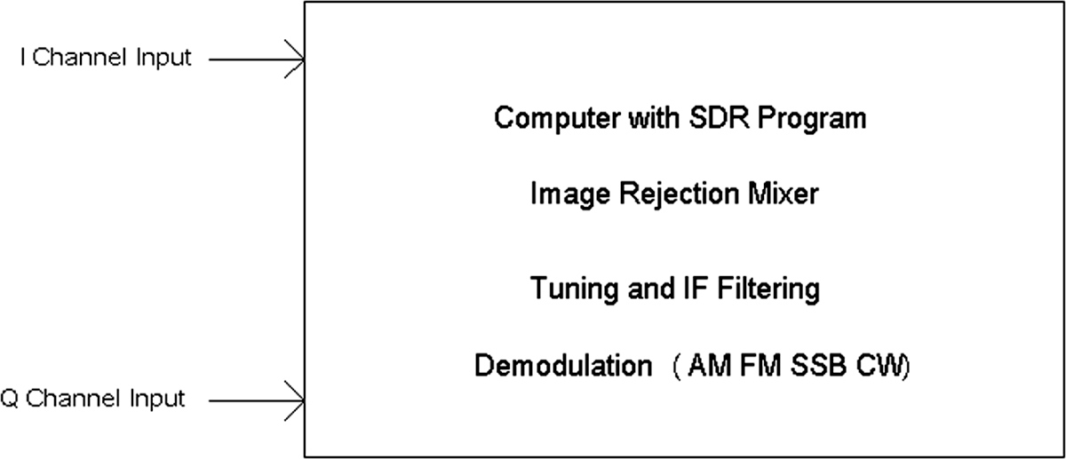
FIGURE 12-1C SDR functions within a computer or system on a chip.
With the I and Q signals, demodulation of broadcast AM signals is achieved by multiplying the I signal by itself and multiplying the Q signal by itself, summing the squares of the I and Q signals to provide a summed signal, and then taking the square root of that summed signal. Although this process may seem mysterious when compared with envelope detection, it is not.
But here is a hint on how this demodulation works: Use the trigonometric identity that [sin(Bt)]2 + [cos(Bt)]2 always is equal to 1 and that the I signal is [1 + m(t)] cos(Bt) and the Q signal is [1 1 m(t)] sin(Bt), where m(t) represents the audio information. Chapter 16 provides a detailed explanation on how AM demodulation works via I and Q signals.
Other functions included in an SDR are demodulation of single-sideband signals and frequency-modulation (FM) signals. And depending on the sampling rate of the sound card, the SDR software program allows for tuning to a bandwidth of half the sample rate or up to the sampling rate of the sound card. For example, if the sound card samples at a rate of 192 kHz, an SDR software program allows tuning over a range of at least 96 kHz or up to 192 kHz. Figure 12-1D shows a screen capture of the Winrad SDR software program running. As seen in the figure, the local oscillator is set for 7,150 kHz in this particular example to tune into the amateur-radio 40-meter band. The tuning spans from 7,054 kHz to 7,246 kHz for a range of 192 kHz. Since amateur radio traditionally has single-sideband transmission on the lower sideband for the 40-meter band, lower sideband (LSB) is chosen for the demodulation.
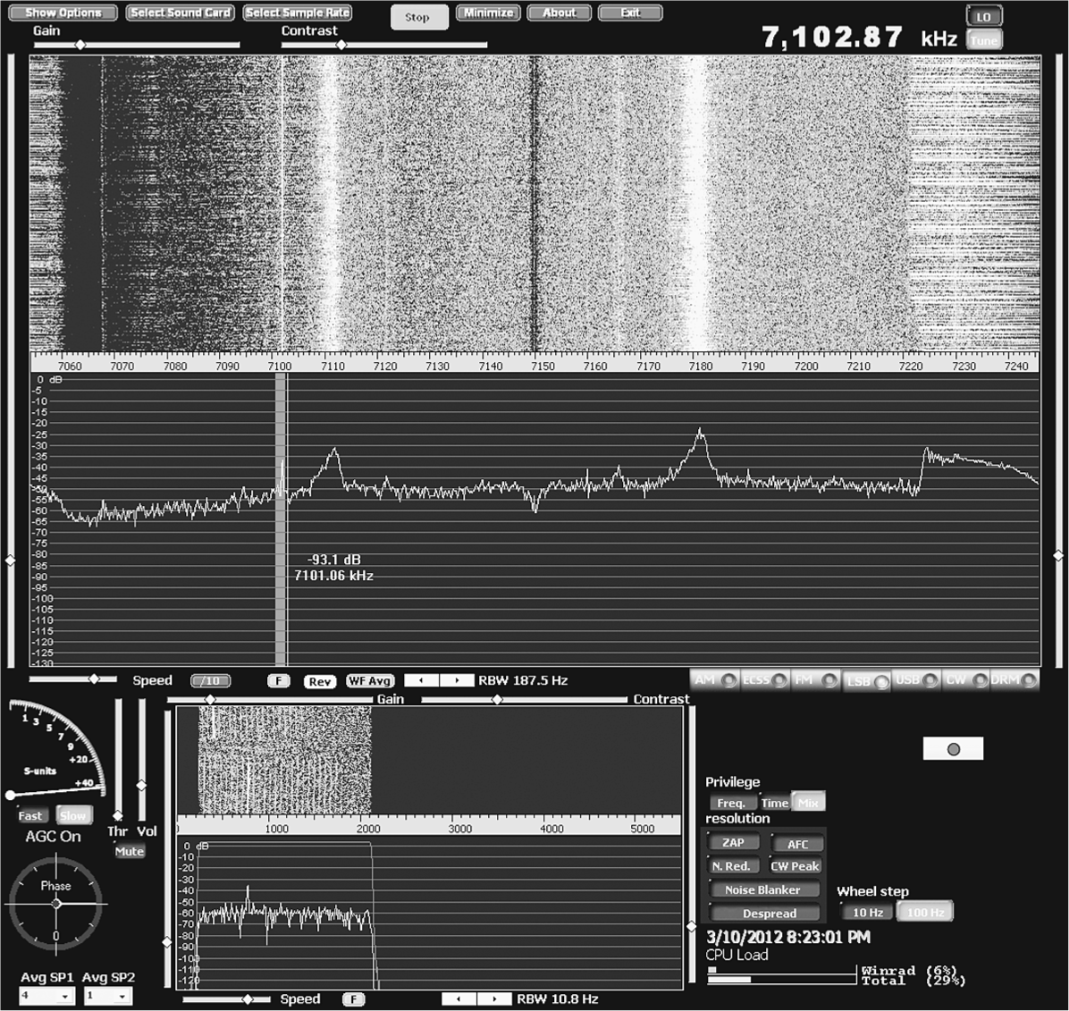
FIGURE 12-1D A screen capture of Winrad showing that at 192-kHz sampling frequency, tuning for radio stations spans 192 kHz.
In this example, 192 kHz of tuning range is available because of the computer’s sound card. Not all computers will come with this “extended” capability. For example, many laptop computers will only allow for 48 kHz or 96 kHz of tuning range. The user can first run Winrad to confirm the sampling rate and tuning range. If the tuning range seems restricted, go to the Winrad top menu to select the sampling rate (Figure 12-1E).

FIGURE 12-1E Selecting sampling rate via Winrad.
Should the sampling rate top out at a number lower than 192,000, upgrading the sound card to a 192-kHz sampling rate is recommended. However, in an SDR, it is still possible to have very usable tuning results with existing sound cards with sampling rates of 44.1 kHz, 48 kHz, or 96 kHz. One solution is to obtain a variable-frequency oscillator such as a direct-digital-synthesis (DDS) generator, which is available in kit or completed form. The DDS generator can tune to the stations instead of the Winrad software program.
SDR Front-End Circuits, Filters, and Mixers
As stated previously, the SDR front-end circuits usually require some type of filter prior to mixing or down-converting to the low-frequency IF signal for the computer to process. The filter generally must cut off or attenuate low-frequency noise in the IF band of about 100 kHz and below. Therefore, the simplest filter can consist of a high-pass filter with a cutoff frequency at about 200 kHz to 100 kHz. With a high-pass filter, low-frequency noise such as power-line hum can be attenuated effectively so that the demodulated signal does not include this type of low-frequency noise.
However, ideally, the filter should be a combination of a high-pass filter and a low-pass filter in which the low-pass filter prevents signals from out of the band of interest to be demodulated. The low pass filter is especially required if the SDR front-end circuit includes a switch mode RF mixer. A switch mode RF mixer is also a harmonic mixer which means that RF signals near a harmonic of the local oscillator or switching frequency will also mix down to the IF. Examples of switch mode mixers include commuting mixers and sampling circuits. It should be noted that a band-pass filter has a high-pass and a low-pass filtering characteristic. Thus, at a minimum, a single-inductor/capacitor (LC) band-pass circuit should be used for filtering. But a multipole band-pass filter may be used for wider bandwidth and sharper cutoff characteristics.
More elaborate filters usually result in better noise performance and overload characteristics, though. More filtering restricts the signals to a smaller portion of the RF spectrum and thus removes interfering signals for “jamming,” or overloading, the mixer.
Figure 12-2 presents examples of simple LC and multistage band-pass filters. The circuits located at the top portion of the figure illustrate a simple LC band-pass network, whereas the circuit at the bottom shows a multistage LC band-pass filter for sharper cutoff to out-of-band signals and noise.
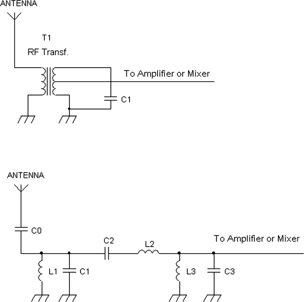
FIGURE 12-2 Simple LC and multistage band-pass filter for an SDR front-end circuit.
In terms of simplicity for mixing or down-converting the RF signal to a low-frequency IF signal, a commutating switch such as the one used in the coil-less radio in Chapter 11 works very well in terms of handling high-level RF signals as well as in terms of low noise performance.
In addition, a sampling circuit provides RF mixing action. For example a sample-and-hold circuit can serve as a mixing circuit. For those who have experimented with digitizing audio signals, one knows that aliasing can occur when the input signal’s frequency exceeds half the sampling frequency. For example, if a digital audio system is sampling at 44.1 kHz, then an input signal of 25 kHz connected into the analog-to-digital converter will cause a 19.1-kHz aliasing signal to appear at the output. But the 19.1-kHz signal is just a signal that has a difference frequency of the sampling frequency and the input frequency or, alternatively stated, 44.1 kHz – 25 kHz = 19.1 kHz. So the sampling circuit can be used as a mixer.
Figure 12-3A shows a commutating switching mixer. The commutating mixer has been used since at least around 1930. This mixer circuit switches between a noninverting output RF signal and an inverting output RF signal. So a push-pull or complementary analog (RF) signal is needed at the inputs of this mixer. Under ideal conditions, this particular mixer is balanced in that neither the input RF signal nor the oscillator signal appears at its output terminal. However, in practice, there is a very small leak-through of the RF and oscillator signals at the output.

FIGURE 12-3A Commutating switch-mode mixer.
As mentioned previously, sampling a signal is a form of mixing or multiplication. And in particular, a sample-and-hold circuit allows for the equivalent of peak detection such that the sampled output of the mixer generates an IF signal that has almost the same amplitude as the input RF signal.
Figure 12-3B shows a single sampling switch with a hold capacitor C. Two or more sample-and-hold circuits may be used to generate I and Q signals. In its simplest form, two of these circuits will provide 0- and 90-degree phase-shifted signals.
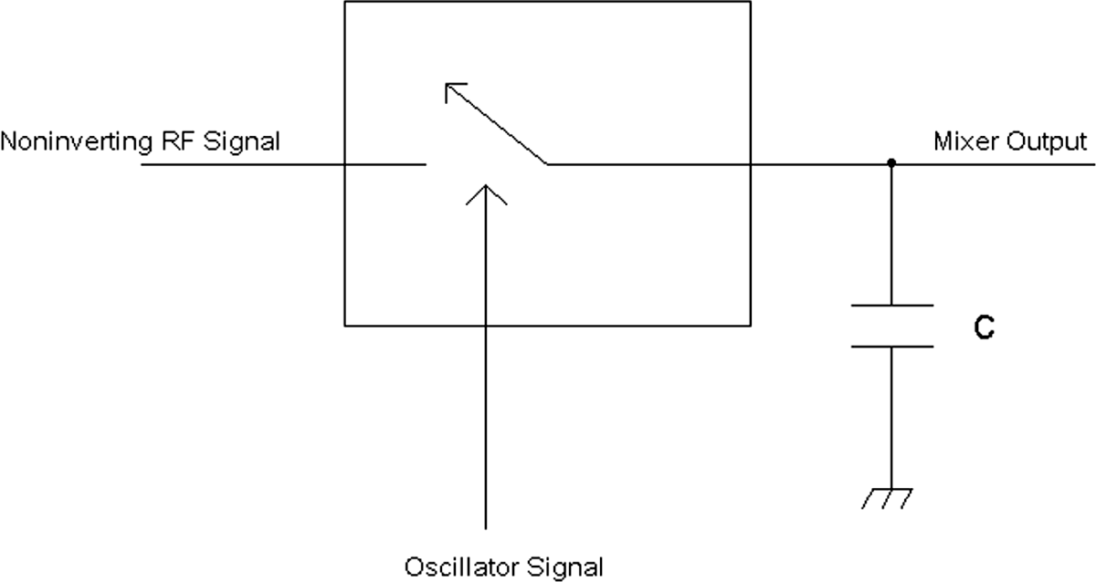
FIGURE 12-3B A sample-and-hold circuit that can be used for RF mixing.
In another configuration using a four-pole sample-and-hold circuit designed by Dan Tayloe, I and Q signals also can be generated. A variant of the four-pole sample-and-hold circuit can be implemented by using four single-sampling switches and capacitors. One should note that the sampling mixer is very popular with SDR do-it-yourself (DYI) kits.
Phasing Circuits for 0- and 90-Degree Outputs for I and Q Signals
To generate I and Q signals, a circuit or series of circuits must be used to generate two outputs for a signal whose frequency range is defined. For SDR software programs, ideally, a phasing circuit should provide 0- and 90-degree outputs up to one-half the sampling rate of the sound card. For example, a sound card that samples up to 192 kHz will require that the phasing circuit provide a constant difference of 90 degrees from the I and Q outputs over a range of up to 192 kHz/2 = 96 kHz.
Most practical analog phasing circuits work over a range of frequencies that are defined as the lower and higher limit frequencies. For example, the lower limit frequency cannot be at 0 Hz or near DC (direct currect) but must be some positive number frequency such as 10 Hz or 300 Hz. The upper frequency limit theoretically can be as high as the designer wants, and this upper limit depends on the bandwidth of the amplifiers or components used.
Figure 12-4 presents a basic analog 0- and 90-degree phase-shift system. This phasing system must have two characteristics. Over the frequency range from the lower to the higher frequency limits,
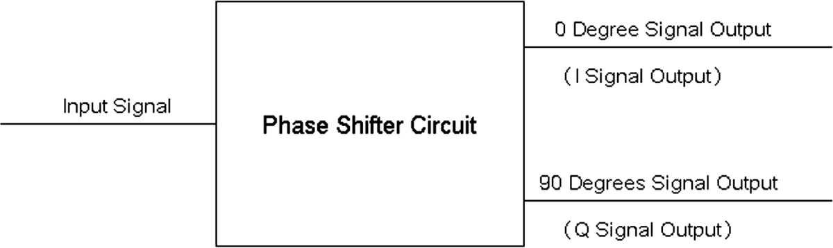
FIGURE 12-4 A phasing system with a single input terminal and two outputs for I and Q signals.
1. The I and Q outputs must maintain constant amplitude relative to each other.
2. The I and Q outputs must maintain a constant 90-degree difference in phase.
Any amplitude variation or deviation from the 90-degree phase difference between the I and Q outputs over the frequency range will cause the image-reject mixer in the computer to not completely reject the image signal.
Figure 12-5 provides an example phasing circuit that generates 0- and 90-degree output.
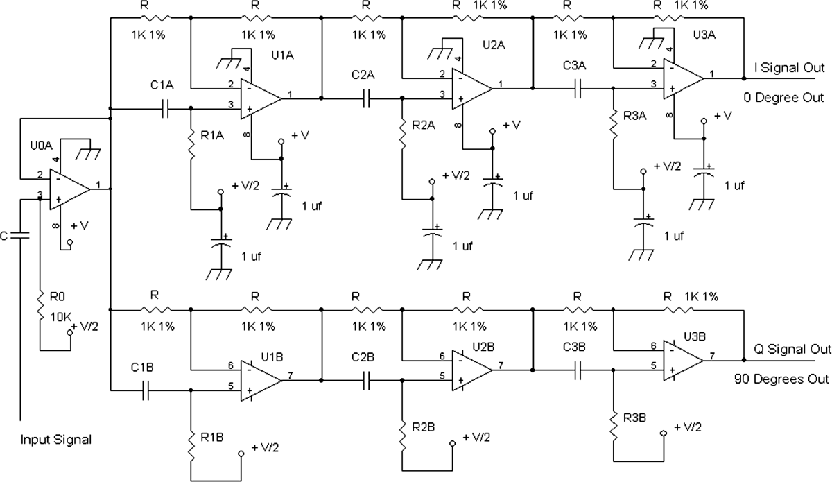
FIGURE 12-5 An analog phase-shifting circuit that provides I and Q signals.
Before I explain operation of this phasing circuit, I would like to recommend a terrific book on synthesizing filters and phase-shift networks by Arthur B. Williams. It is called the Electronic Filter Design Handbook and is published by McGraw-Hill. Any edition (e.g., the 1980 First Edition, 1989 Second Edition, 1995 Third Edition, or the 2006 Fourth Edition) of this book will be helpful. And it is from this book that the phasing circuit in the figure is taken. I cannot say enough about how great this book is in terms of showing how to design all types of filters with coils or active components. The gyrator circuit in Chapter 11 came from this book. Any hobbyist or engineer will find that this book contains practical designs without long mathematical derivations on filter design. In short, this is a great filter book for designers.
Figure 12-5 shows a phase-shifting circuit with six amplifiers: U1A, U1B, U2A, U2B, U3A, and U3B.
![]()
A low-output-impedance amplifier (e.g., op amp U0A) should drive the resistors and capacitors associated with U1A and U1B.
Each amplifier section constitutes an all-pass network. So the output of any of the amplifiers will provide constant amplitude over frequency while phase shifting the input signal. The actual phase shift varies with the frequency of the input signal. So the output of the A section of amplifiers at U3A is the summation of phase shifts from U1A, U2A, and U3A. Each amplifier has a different RC time constant, such as C1A R1A, C2A R2A, and C3A R3A. These time constants cause the phase (as compared with the input signal) at the output of U3A to vary quite “wildly” as the frequency is varied. At first glance, this may look all wrong. But there is the B section that also generates phase shifts from U1B, U2B, and U3B in a similarly “wild” manner but with a constant difference of 90 degrees from the A section.
The amplifier gain resistors R are identical 1 percent resistors and can be in the range of 1,000 ![]() to 10,000
to 10,000 ![]() as long as the resistors are the same value for each amplifier. So, for example, all the resistors R can be 1,000
as long as the resistors are the same value for each amplifier. So, for example, all the resistors R can be 1,000 ![]() 1 percent (or better, such as 0.25 percent tolerance).
1 percent (or better, such as 0.25 percent tolerance).
So we have one set of phasing circuits in the A section and another set in the B section, both generating lots of phase shift when compared with the input. But by carefully designing the RC time constants for each amplifier, a 90-degree phase difference is achieved with constant amplitude for an input signal having a lower and higher frequency limit.
The phasing circuit in Figure 12-5 maintains a constant 90-degree phase difference over a frequency range. This range can be expressed as the ratio of the higher frequency limit to the lower frequency limit. For example, from the Arthur B. Williams book, the following values are calculated for a ratio of the higher frequency limit to the lowest frequency limit of about 10:1 for a frequency range of 300 Hz to 3,000 Hz with an error of about 0.1 degree. And it should be noted that although 300 Hz to 3,000 Hz typically is a range for a single-sideband audio phase shifter, for the SDR, a range of about 3,000 Hz to 30 kHz is more useful.
In order to scale the original range of 300 Hz to 3,000 Hz to a new range, just scale either the resistors or the capacitors coupled to the positive (+) terminal of the amplifier to the reciprocal of the scaling factor. For example, if 3,000 to 30,000 Hz is needed, then this is a scaling factor of 10. So just divide all the resistor values at the (+) terminal of the amplifiers by 10, or alternatively, divide all capacitor value at the (+) terminal of the amplifiers by 10.
![]()
Do not divide both the values of the resistors and capacitors.
Table 12-2 illustrates a phase-shifting circuit that holds a 90-degree phase difference within about ±0.1 degree.
TABLE 12-2 Resistor and Capacitor Values for the Phase-Shifting Circuit that Maintains a 90-Degree Phase Difference between the I and Q Signal Outputs within 0.1 Degree
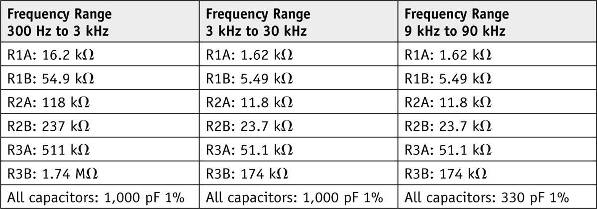
The first column of the table shows the original resistor and capacitor values for a frequency range of 300 to 3,000 Hz. To scale the frequency range 10-fold for 3 to 30 kHz, the resistors are divided by 10, but the capacitors remain the same. The third column shows how to scale the frequency range of 3 kHz to 30 kHz to 9 kHz to 90 kHz simply by taking the (same) resistor values of the second column and dividing the capacitor values by 3 (1,000 μF/3 = ~ 330 μF).
Op amps for these circuits (in Table 12-2) should have at least a 10-MHz gain bandwidth product. For example, an AD823 op amp may be used. For the values shown for the frequency ranges of 3 kHz to 30 kHz and 9 kHz to 90 kHz, one can use an NE5532 or LM833 op amp.
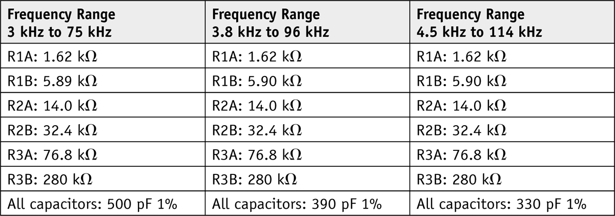
And see Table 12-3 for a phase-shifting circuit that holds the 90-degree phase differential between I and Q channels within ±0.44 degree but over a frequency ratio of about 25:1 instead of the 10:1, as seen in Table 12-2. For the values shown in the table, the op amps used may be NE5532 or LM833.
TABLE 12-3 Resistor and Capacitor Values for the Phase-Shifting Circuit that Maintains a 90-Degree Phase Difference between the I and Q Signal Outputs within 0.44 Degree
A question one may ask is, What is the consequence when the 90-degree difference in phase between the I and Q channels is off by a degree or two? That is, if the I and Q channels are 89 or 88 degrees in phase difference, what happens? It turns out that an image-reject mixer relies on a precise 90-degree phase differential in order to perfectly cancel out the image signal. An error of a degree or two causes an imprecise cancellation of the image signal, and thus some of the image signal will appear at the output of the image-reject mixer.
For a rough approximation, the residual image signal output can be expressed by the following:
![]()
where x is the error phase angle measured in radians. Note that 1 radian = 57.3 degree, so 0.1 radian = 5.73 degrees, and 0.01 radian = 0.573 degree.
For small values of x measured in radians that are much smaller than 1,
![]()
For example, if x = 0.1 radian, then sin(0.1) ~ 0.1. Again, recall that x is measured in radians. And for all practical purposes, if x = 0.01, then sin(0.01) = 0.01. And again, to reiterate, x is measured in radians, and x [in the equation of sin(x) = x for small values of x] is not measured in degrees.
Also, 1 degree equals 0.0174 radian. So a 1-degree error will result in a residual image signal of about
whereas a 0.5-degree error from the 90-degree difference phase between the I and Q channels will result in a 0.435 percent leak-through of the image signal.
For an appropriate approximation of the residual image signal output with a phase error or deviation from the 90 degree difference between the I and Q channels is 1 percent per 1 degree of phase error, see Chapter 21, which presents an analysis of an image-reject mixer and provides further details pertaining to phase error.
Multipliers for Generating 0- and 90-Degree Phases
While the phase-shifting circuit in Figure 12-5 provides an accurate phase difference of 90 degrees between the I and Q channels, its accuracy depends on precision parts. Also, to increase the range of frequencies, more amplifier stages must be added. For example, if a frequency ratio of 500:1 is needed with less than 0.5 degree of error, 10 amplifiers instead of the 6 shown in Figure 12-5 will be required.
So an alternative to phase-shifting networks is to use multiplier circuits. Chapters 8 and 9 showed that a mixing circuit creates a multiplying effect on two signals. And one of the outputs of the mixing circuit is a signal that has a frequency equal to the difference of the two input signals—the local oscillator signal and the RF signal.
But what if we connect the RF signal to two multipliers, and each multiplier is connected to an oscillator of the same frequency, and one of the multiplier has a phase-shifted oscillator signal? See Figure 12-6.
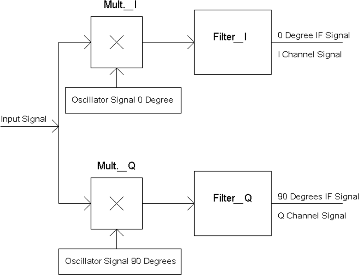
FIGURE 12-6 An alternative method of providing a 0- and a 90-degree output for I and Q signal generation.
It turns out that when two signals are multiplied to provide a difference-frequency signal, the phase of one or both of the two signals carries over to add a phase shift to the difference-frequency signal. So, if a mixer generates a signal that has a difference frequency (F1 – F2), then it also carries over the phase angle. That is, if signal 1 = cos(F1t + Φ) and signal 2 = cos(F2t), then the resulting difference-frequency signal by multiplication is
![]()
where A is a scaling factor–based conversion gain of the multiplier, and f is the phase angle, such as 90 degrees.
So in Figure 12-6 the top multiplier has the RF signal multiplied by a cosine waveform, and the bottom multiplier has the RF signal multiplied by a 90-degree-shifted cosine waveform or a sine waveform. The output of both top and bottom mixers will provide a signal with the exact same difference frequency (frequency of the RF signal minus the frequency of the cosine waveform). However, the bottom mixer will provide a difference-frequency signal with a 90-degree phase shift in relation to the difference-frequency signal from the top mixer.
The output of each mixer then is connected to a filter to pass the difference-frequency signal while removing other signals, such as a signal whose frequency is the sum of the frequencies of the RF and cosine waveform. Thus the outputs of the (identical) filters provide I (0-degree) and Q (90-degree) signals, which typically are low IF signals (e.g., <100 kHz) for the SDR.
One advantage of multiplying mixers to generate I and Q signals is that there is essentially no lower- or higher-limit frequency to worry about. So, if the frequency ratio changes from 10:1 to 1,000:1 in maintaining 90 degrees of phase shift between the two channels, the multiplier circuit in Figure 12-6 does not change, whereas the phase-shifting circuit shown in Figure 12-5 increases in complexity.
One small downside to using switching mixers versus a phase-shifting network is that the signal generator driving the switching mixer initially has to run at four times the local oscillator frequency. If an oscillator has a perfect square wave with 50 percent duty cycle, then the signal generator can run at twice the local oscillator frequency. In order to synthesize a 90-degree phase-shifted version from the generator, at least twice the local oscillator frequency is needed for a digital divider circuit.
Example Radio Circuits for Software-Defined Radios
For a first experiment in an SDR, an AM radio will be shown. It will contain some circuits that were shown in previous chapters but will have a lower IF signal for inputting to a computer’s sound card.
Figure 12-7 presents a block diagram of an AM radio front-end circuit for an SDR. The figure shows an AM radio with a built-in loop antenna that couples RF signals into an RF transformer. The RF transformer tunes with a variable capacitor to pass frequencies of the tuned stations while removing signals outside the standard AM band. Since a switch-mode mixer will be used, removal of signals outside the AM band is essential. However, the variable tuned circuit, variable capacitor VC1_RF and an inductor T1, does not have the narrow bandwidth to reject image signals because of the low IF of less than 20 kHz. Fortunately, via the I and Q signals fed to the computer, the image signals will be rejected (or selected) via the digital signal-processing algorithms in the software.

FIGURE 12-7 A front-end block diagram for an SDR that tunes the standard AM band.
The switch-mode mixer also is connected to a local oscillator tuned via VC1 Osc that is set to about 15 kHz above the tuned RF signal such that the output of the mixer circuit provides a low IF of about 15 kHz. The 15-kHz IF signal from the mixer is connected to a phase-shifting circuit similar to the one in Figure 12-5. And the I and Q outputs of the phase-shifting circuit then are coupled to the audio inputs of a sound card in a computer. As stated previously, tuning is accomplished mostly by the variable capacitor, so the entire 1-MHz range of the broadcast AM band can be accessed. Thus the 192-kHz tuning range of the computer via Winrad and the sound card is insufficient for tuning across the entire AM band.
The SDR program Winrad then is used to detect the I and Q signals, which then provide audio signals to the speakers in the computer.
Parts List
• C1, C2, C3, C4, C6, C8, C24: 0.01 uF
• C5, C11, C12, C18, C22, C25: 33 μF, 16 volts
• C7, C9: 0.001 μF, 5% film
• C10, C23: 0.01 μF, 5% film
• C13: 5 pF for R22 = 220 k![]() ; or 47 pF for R22 = 22 k
; or 47 pF for R22 = 22 k![]()
• C14, C16, C17, C19, C20, C21: 500 pF 1%
• C15, C26, C27, C28, C29, C30: 1 pF, 35 V
• R1, R2, R4, R5, R7, R8: 12 k![]()
• R3: 2 M![]()
• R6: 4.7 ![]()
• R9: 1,800 ![]()
• R10: 1,000 ![]()
• R11, R13, R14, R16, R17, R19, R23, R25, R26, R28, R29, R31: 1,000 ![]() 1%, 0.5%, or 0.25%
1%, 0.5%, or 0.25%
• R12: 1,620 ![]() 1%
1%
• R15: 14.0 k![]() 1%
1%
• R18: 76.8 k![]() 1%
1%
• R20, R32: 100 ![]()
• R21: 22 k![]()
• R22: 220 k![]() , or 22 k
, or 22 k![]() for lower gain so as to reduce overloading the sound card
for lower gain so as to reduce overloading the sound card
• R24: 5.90 k![]() 1%
1%
• R27: 32.4 k![]() 1%
1%
• R30: 280 k![]() 1%
1%
• T1: 42IF100, 42IF110, or 42IF300
• T2: 42IF100, 42IF110, or 42IF300 primary winding or 330-μH variable inductor
• VC1: twin-gang variable capacitor 270 pF and 270 pF
• Loop antenna to low-side tap of T1
• U1: 74HC04
• U2: UA733 or LM733 video differential amplifier
• U3: 74HC4053 or 74HCT4053
• U4, U5, U6, U7: NE5532 or LM833
• U8: LM78L05
![]()
Before building the circuit, with an inductance meter, set T1’s primary winding inductance value across the main winding (e.g., do not measure at the tap of T1 or T2) to 322 μH, and set T2’s inductance value to 312 μH. This will ensure that the oscillator’s frequency is at least 10 kHz higher than the tuned RF frequency with T1.
Figures 12-8A and 12-8B show circuit diagrams for experimental AM front circuits for an SDR.

FIGURE 12-8A Schematic diagram of an AM radio front-end circuit for an SDR that includes a commutating mixer.

FIGURE 12-8B Schematic diagram of an AM radio front-end circuit with the analog phase-shifting circuit.
Before proceeding with building this circuit, with an inductance meter, adjust the inductance value of T1’s primary winding to 322 μH and T2 to 310 μH. Radio signals are tuned via VC1 RF and T1 to provide the RF signals to amplifier U2, which has noninverting and inverting analog signal outputs to the commutating mixer, U3. The mixer U3 is switched via the local oscillator signal from U1B, whose frequency is between 10 kHz to 20 kHz above the frequency of the tuned RF signal. The output of mixer U3 then is low-pass-filtered via R9 and C7 to provide a low-frequency IF signal in the range of 10 kHz to 20 kHz. This low-frequency IF signal is coupled to an IF amplifier, U4A, to further amplify the IF signal. The amplified IF signal then drives two banks of phase-shifter circuits to provide I and Q signal outputs. The I signal via U7A and the Q signal via U7B then are connected to the line input of the sound card of a computer with an SDR software program running. With the SDR program running, select “AM” for the demodulation and a demodulated bandwidth of 3 kHz to 5 kHz. Then, via the software program, tune for a radio station between 10 kHz and 20 kHz. To tune throughout the AM band range of 540 kHz to 1,600 kHz, adjust variable capacitor VC1.
The value of R22 may be selected to adjust the signal amplitude to match the requirements (e.g., input sensitivity) of individual sound cards. For some sound cards, R22 set to 220 k![]() may cause overloading. Thus R22 can be replaced with a 22-k
may cause overloading. Thus R22 can be replaced with a 22-k![]() resistor to reduce the I and Q signals by 10. Note that C13 should be replaced with a 47-pF capacitor if R22 is 22 k
resistor to reduce the I and Q signals by 10. Note that C13 should be replaced with a 47-pF capacitor if R22 is 22 k![]() .
.
Alignment procedure: With a reference generator of a known frequency, such as the 537-kHz reference RF oscillator shown in Chapter 4, couple the generator’s signal with a wire near the loop antenna. With an oscilloscope set to alternating-current (AC) coupling, probe either end of C3 or C4, and tune VC1 for maximum signal. Then connect a frequency counter to pin 4 of U2 and adjust T2 (or an adjustable inductor) to a frequency about 15 kHz above the RF oscillator’s frequency. For example, if the RF oscillator is measured at 537 kHz, then adjust T2 such that pin 4 of U2 reads 552 kHz.
Figure 12-9A shows a screen capture of the Winrad program with the AM radio front-end circuit connected to a computer with a received radio station. In the figure, the tuned desired signal is highlighted by a wide vertical strip, whereas the image signal is highlighted by a vertical line. The image signal is about 40 dB lower than the desired signal (tuned signal). Or stated another way, the amplitude of the image signal is about 1 percent of the amplitude of the desired signal (tuned signal).
FIGURE 12-9A Screen capture of Winrad program with default adjustments for nulling out the image signal.
The Winrad program allows for fine adjustment to null out the image signal (Figure 12-9B). By clicking on the “Show Options” tab and scrolling down to “Channel Skew Calibration,” fine adjustments can be made for both amplitude and phase to null out the image signal. See the vertical line in the screen capture where the image signal is attenuated into the noise floor.

FIGURE 12-9B Image signal reduced further by adjusting amplitude and phase within the Winrad software program.
Second SDR Front-End Circuit for the 40-Meter Amateur Radio Band
Figure 12-10 shows a block diagram of an experimental front-end circuit for down-converting RF signals around 7.150 MHz to a low-frequency IF signal with I and Q output signals. Because the local oscillator will provide a fixed frequency, the I and Q output signals preferably are digitized at the highest sampling rate to provide the widest tuning range. For example, a 192-kHz rate allows tuning over a frequency range of 192 kHz via a software program such as Winrad. Fortunately, the 40-meter amateur radio band for voice transmission occupies approximately a 150 kHz of bandwidth for the frequency range 7.150 MHz to 7.300 MHz.

FIGURE 12-10 Block diagram of the experimental front-end circuit for the 40-meter band.
RF signals from an antenna are coupled to a 7.150-MHz band-pass filter. The output of the band-pass filter is buffered by an amplifier to drive the inputs of four analog switches. The analog switches are controlled by a four-phase oscillator signal that is used to make the four analog switches sample at 0, 90, 180, and 270 degrees. By sampling at 0 and 180 degrees, an I channel is provided. Similarly, by sampling at 90 and 270 degrees, a Q channel is provided. The output signals from the mixer are further amplified to provide I and Q signals of suitable amplitude for the computer’s sound-card input circuits.
Parts List
• C1, C8, C9: 1 μF, 5% film, note: C1 can be 0.01 μF
• C2: 47 pF
• C3: 22 pF or 27 pF
• C4, C5, C6, C7: 0.0047 μF, 5% film
• C10, C12, C15, C16, C17, C18, C24: 0.01 μF
• C11, C13, C14, C22, C23: 33 μF, 25 volts
• C19, C20: 22 pF or 33 pF
• C21: 1 μF, 35 volts
• R1: 11 k![]()
• R2: 39 k![]()
• R3: 47 ![]()
• R4: 470 ![]()
• R5: 22 ![]()
• R6, R12, R13, R16: 100 ![]()
• R7: 3,300 ![]()
• R8, R10: 1 k![]() 1%
1%
• R9, R11: 100 k![]() 1%
1%
• R14: 1 M![]()
• R15: 330 ![]()
• T1: 10.7-MHz IF transformer 42IF129
• Y1 crystal: 28.636 or 28.322 MHz fundamental frequency crystal
• U1: 74HC4066
• U2, U3: NE5532 or LM833
• U4: 74AC04
• U5: 78L05 or 7805
• U6, U7: 74AC74
• U8: 74AC08
• Q1: MPHS10
• Q2: 2N3906
Figures 12-11A and 12-11B present schematic diagrams of the front-end circuit for receiving 40-meter RF signals. Note that this circuit can operate from a regulated 9-volt to 12-volt DC supply or a battery.

FIGURE 12-11A Schematic diagram of an experimental 40-meter RF circuit for an SDR local oscillator circuit with four-phase oscillator signals.
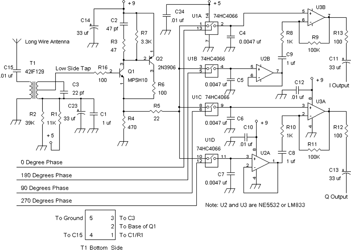
FIGURE 12-11B Schematic diagram of the front-end circuit including front-end input filter and mixing circuit.
An antenna is coupled to a low-impedance winding of an RF transformer T1, which is really a 10.7-MHz IF transformer with an added capacitor C3 to lower the resonating frequency to 7.22 MHz. T1 as configured in this circuit has an input impedance of about 50 ![]() for matching to an antenna. The other side of T1 at the low-side tap has about a 1:10 turns ratio, which then provides about a 10-fold increase in RF signal when compared with the signal at the antenna input terminal. To drive the analog switch mixer, the signal from the low-side tap of T1 is buffered by a compound complementary transistor amplifier Q1 and Q2. This amplifier provides a high-impedance input resistance so that the Q of T1 is not affected and so that the amplifier also provides a low output resistance capable of driving the mixing circuit consisting of four sample-and-hold switches in U1.
for matching to an antenna. The other side of T1 at the low-side tap has about a 1:10 turns ratio, which then provides about a 10-fold increase in RF signal when compared with the signal at the antenna input terminal. To drive the analog switch mixer, the signal from the low-side tap of T1 is buffered by a compound complementary transistor amplifier Q1 and Q2. This amplifier provides a high-impedance input resistance so that the Q of T1 is not affected and so that the amplifier also provides a low output resistance capable of driving the mixing circuit consisting of four sample-and-hold switches in U1.
![]()
To adjust T1, connect a 7.22-MHz signal to C15, and measure with an oscilloscope the signal output at the emitter of Q1 [MPSH10, and note the pin-out for this transistor (BEC), which is different from a 2N3906 (EBC)]. Then adjust T1 for maximum signal level.
The control pulses that turn on the switches in U1A–U1D are nonoverlapping pulses, being a quarter cycle in duration at 0-, 90-, 180-, and 270-degree relative phases. The sampling frequency of each of these nonoverlapping pulses is the crystal oscillator’s frequency divided by 4. The sample-and-hold signals for 0 and 180 degrees appear at capacitors C4 and C5. An “almost” differential amplifier consisting of U3B and U2B amplifies roughly the difference in voltage across C4 and C5.
The reason for saying that U3B and U2B almost form a differential amplifier is because normally the (+) input of U3B would include a resistive divider circuit. But since there is none, there is an error of about 1/gain. Since the feedback resistors in U6A (and U6B) result in a gain of about 100, the error is about 1/100, or 1 percent. Similarly, the 90- and 270-degree sampled signals are amplified almost differentially by a factor of 100 via amplifier U3A and U2A.
![]()
Taking the difference between the two signals that are sampled 180 degrees apart in Figure 12-11B amounts to essentially the same as the circuit shown in Figure 12-8A, consisting of differential output amplifier (Ua733) U2 coupled to the two input terminals of the single-pole double-throw switch U3A. The output signals in Figure 12-11B of U3B and U3A then provide I and Q signals to the computer’s sound card.
It should be noted that because the gain bandwidth product of the op amps in U6 is 10 MHz, it is operating near the limit to provide a 100-kHz bandwidth for a closed-loop gain of 100. The NE5532 is configured to provide a gain of 100, so the frequency response is 100 kHz, which means that there is very little negative feedback at 100 kHz. Normally, this can be a problem because the gain and frequency response of amplifiers are not tightly specified. That is, only a minimum specification of the gain bandwidth product of the op amp is guaranteed. So, if U6, a dual op amp, were replaced by two single op amps of similar specifications, chances are that the I and Q channels would suffer a mismatch in frequency response and ability to maintain a 90-degree phase difference over the range of frequencies (e.g., 100 kHz). But because in a dual op amp the characteristics in the die are matched (e.g., equally bad or equally good on both op amps in the package), it is often possible to still have good matching on the I and Q channels. Of course, higher-frequency dual op amps can be used in place of the NE5532.
In reference to Figure 12-11A, the crystal oscillator at about 28.6 MHz runs at four times the mixing frequency but gets frequency divided by 2 via U1A to ensure a 50 percent duty-cycle square wave at 14.3 MHz. This 14.3-MHz square-wave signal will be used later to generate a 90-degree phase-shifted version of the 7.150 MHz. A second frequency-divider circuit U2A further frequency divides the 14.3-MHz signal from U1A to provide a 7.150-MHz signal at a reference phase of 0 degree. By feeding this reference phase 7.150-MHz signal to a latch flip-flop circuit and clocking the latch with an inverted-phase 14.3-MHz signal, the output of the latch circuit provides a 90-degree phase-shifted signal at 7.150 MHz. The actual frequency of the crystal is 28.636 MHz, which results in 7.159 MHz instead of 7.150 MHz.
The 0- and 90-degree signals from U2A and U2B, along with output signals from U1A, are fed to a decoder circuit consisting of four AND gates, U3. The outputs of the AND gate provide the 0-, 90-, 180-, and 270-degree nonoverlapping signals for the analog switch mixer U4.
This front-end circuit was able to receive single-sideband transmissions on the 40-meter band. However, this circuit is just a starting point. Improvements can be made, and if time permits, another front-end circuit for receiving the 40-meter band will be presented.
It is suggested that the reader may just want to purchase DIY SDR front-end kits. One vendor is SoftRock, which sells receivers and transceivers for the amateur radio enthusiast.

To transmit below the 10-meter band (i.e., transmit below 28 MHz), the reader must hold at least a general class amateur radio license. And to transmit on any amateur radio band, a license is required. Consult the ARRL, the Amercian Radio Relay League, at www.arrl.net for more information on licensing.
If the reader is just interested in operating receivers, no license is required. And SoftRock sells many receiver kits.
Well, this ends the first part of this book, which is geared more for the hobbyist to just build or experiment with radio circuits. It has been an interesting ride for the last 12 weeks for me in designing, building, testing, and writing about radio circuits.
The second part of this book will concentrate on tutorials of various subjects related to electronics, so I hope that readers will stick around for that. I will do my best to explain some of the principles of electronics with no more than high school math. So hang on, there is more to come.