Chapter 11
Inductor-less Circuits
In previous chapters there was extensive use of coils, inductors, or transformers for radiofrequency (RF) and intermediate-frequency (IF) signals. This chapter presents alternatives to coils or inductors.
Ceramic Filters
Ceramic filters emulate high-Q inductor/capacitor (LC) circuits as band-pass filters. These filters generally are three-terminal devices with input, ground, and output terminals. However, ceramic filters also are made as two-terminal devices.
The earliest use of ceramic filters for amplitude-modulated (AM) transistor radios can be found in the 1960s. For example, the Motorola Model XP3CE and Model XP4CE 9- and 11-transistor radios from 1965 to 1967 each used a two-terminal ceramic filter in the first IF amplifier. Normally, the first IF amplifier has an RF bypass capacitor from the emitter to ground. In these Motorola radios, the RF bypass capacitor is replaced with a two-terminal ceramic filter, which acts like a series resonant 455-kHz tank circuit. Thus at 455 kHz, the two-terminal ceramic filter has a minimum impedance or resistance, and at frequencies outside 455-kHz band, such as 470 kHz, the ceramic filter has a high impedance. By replacing the RF bypass capacitor with the two-terminal ceramic filter at the emitter of the common-emitter IF amplifier, the output current from the IF amplifier is peaked at the IF frequency and lowered at frequencies outside the IF band.
Two-terminal ceramic filters should not be confused with the very common two-terminal ceramic resonators. A ceramic resonator has a very narrow bandwidth that generally is not suitable for an IF filter used in a standard AM radio. However, because ceramic resonators have very narrow bands, they can be used as a continuous-wave (CW) IF filter for receiving Morse code. Ceramic resonators generally are used for generating frequencies such as seen in one of the generator circuits in Chapter 4. For this chapter, we will concentrate on (wider-bandwidth) ceramic filters instead because resonators exhibit very narrow band characteristics that are not suitable for broadcast AM receivers.
Today, two-terminal ceramic filters are not that readily available, but three-terminal ceramic filters are found commonly. Three-terminal ceramic filters for the AM band could be found in stereo receivers in the 1970s, such as the 1973 Sony STR-222.
As the cost of these three-terminal devices dropped, they were very commonly designed into portable or pocket radios by the middle to late 1970s or early 1980s. For example, in 1981, the Sony ICF-200 pocket radio had three-terminal ceramic 455-kHz and 10.7-MHz filters for AM and frequency-modulated (FM) bands.
One characteristic of a ceramic filter is that unlike an inductor, the direct-current (DC) resistance is very high, just like an open circuit. Another feature of a ceramic filter is that it is meant to be driven and terminated by a specified resistance. Most AM band ceramic filters, for example, have driving and terminating resistances from 1,000 V to about 3,000 V. And ceramic filters may be specified for a wide bandwidth such as 10 kHz to a narrow bandwidth of 3 kHz.
Although ceramic filters have a response like a typical LC band-pass filter near the pass-band frequencies, they do suffer from allowing out-of-band signals to pass through. And, in general, the specified frequency response of a ceramic filter includes an IF transformer preceding it to help remove spurious or out-of-band signals such as the local oscillator signal that is from 1 MHz to 2 MHz.
Manufacturers of ceramic filters include Murata, Toko, and Token. Note that AM (and FM) band ceramic filters can be obtained from www.mouser.com.
Figure 11-1 shows a selection of ceramic filters. In the figure, the ceramic filter on the left is a single-element filter, whereas the item on the right is a multiple-element filter. A multiple-element ceramic filter is essentially two or more single-element ceramic filters that are cascaded.
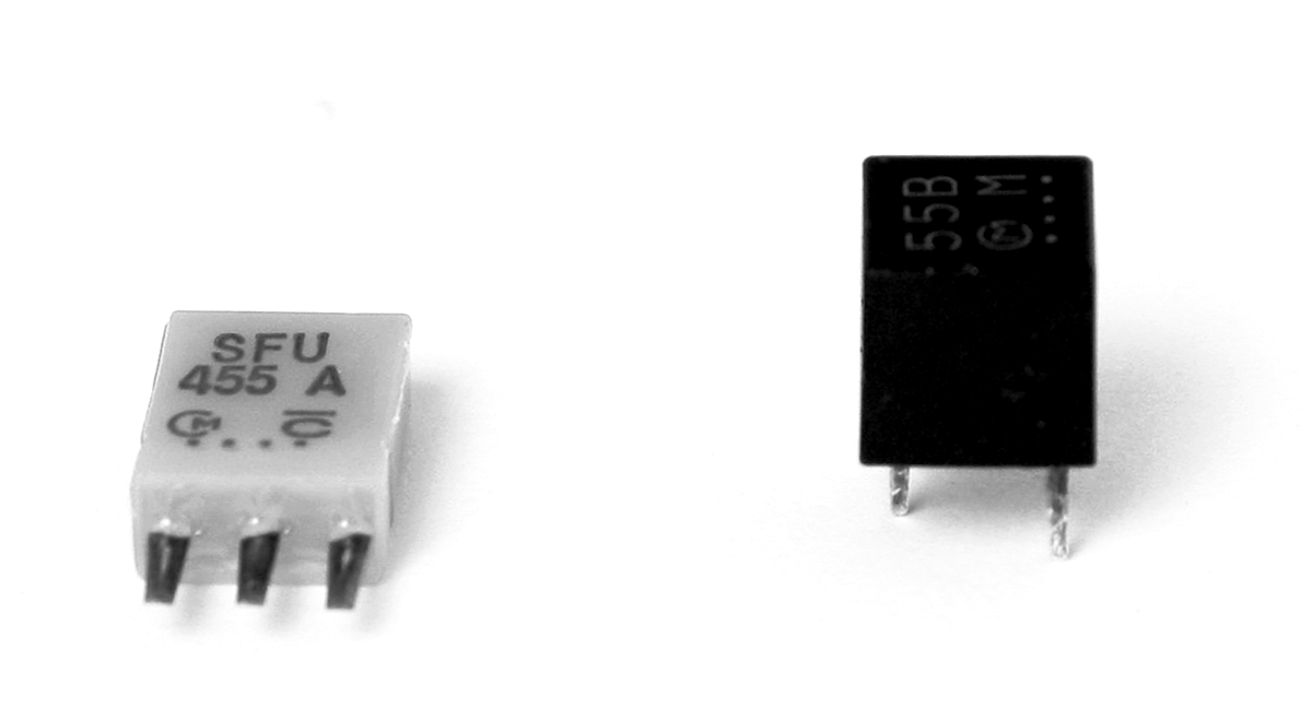
FIGURE 11-1 455-kHz ceramic filters.
![]()
The pin out for the single-element ceramic filter in the lead on the left is the output terminal, and the center lead is the ground or common terminal, and finally, the lead on the right is the input terminal.
Figure 11-2 is a block diagram of a radio with 455-kHz IF ceramic filters. Antenna coil L1 and variable capacitor VC1 provide an RF signal to the converter circuit Q1. Oscillator coil T1 provides a local oscillator signal for converting the incoming RF signal to an IF signal. Ceramic filters extract the IF signal from the output of the converter circuit. The IF signal is filtered and amplified by an IF amplifier circuit. The output of the last IF amplifying transistor Q3 is fed to a diode detector D3 for demodulation.
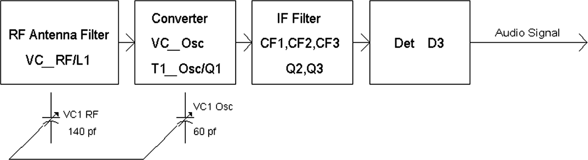
FIGURE 11-2 Block diagram of a radio using ceramic filters.
Parts List
• C1, C3, C7: 0.01 μF
• C2, C4, C8: 1 μF, 35 volts
• C5, C6: 0.15 μF
• R1: 2,200 ![]()
• R2, R5: 3,000 ![]()
• R3, R6, R10: 22 k![]()
• R4, R7, R8: 2,200 ![]()
• R9: 47 k![]()
• L1 antenna coil: 600 μH to 680 μH, 10 to 20 turns for secondary winding
• VC1: two-gang variable capacitor 140 pF and 60 pF
• D1, D2: 1N914
• D3: 1N34 or 1N270
• T1 oscillator coil: 42IF100
• CF1, CF2, CF3: Ceramic filter SFU455A, Murata or equivalent
• Q1, Q2, Q3: 2N3904
Figure 11-3 shows a schematic for an AM radio that uses ceramic filters to replace IF transformers. Received radio station signals are tuned by L1 and VC1 RF to provide RF signals to the base of converter oscillator transistor Q1. Oscillator coil T1 provides a local oscillator signal from about 1 MHz to 2 MHz via coupling the oscillation signal from the secondary to primary windings. A multiplying effect between the RF signal and the local oscillator signal occurs via a large oscillator signal at the emitter of Q1 and a small RF signal at the base of Q1. Thus at the collector of Q1 there is an IF signal as well as a very large-amplitude oscillator signal. Because the ceramic filters have poor rejection for some out-of-band signals, including the oscillator signal, two 455-kHz ceramic filters (CF1 and CF2) are used to extract the 455-kHz IF signal. From the output of ceramic filter CF2 is a usable IF signal for further amplification via the first IF amplifier transistor Q2. The collector terminal output of Q2 is then fed to a single ceramic filter CF3 whose filter output is connected to the input of the second IF amplifier Q3. The output collector terminal at Q3 now provides an IF signal for envelope detection via diode D3. Thus audio signals are provided at C8 for a crystal earphone or the audio signals may be connected to an audio amplifier. Note that D3 is rectifying the negative portion of the AM envelope because the positive portion actually goes into clipping when a strong signal is received. However, the negative portion of the AM envelope at the collector of Q3 is not affected and does not clip. Also, to conserve energy, a power switch may be connected in series with the battery or power source.
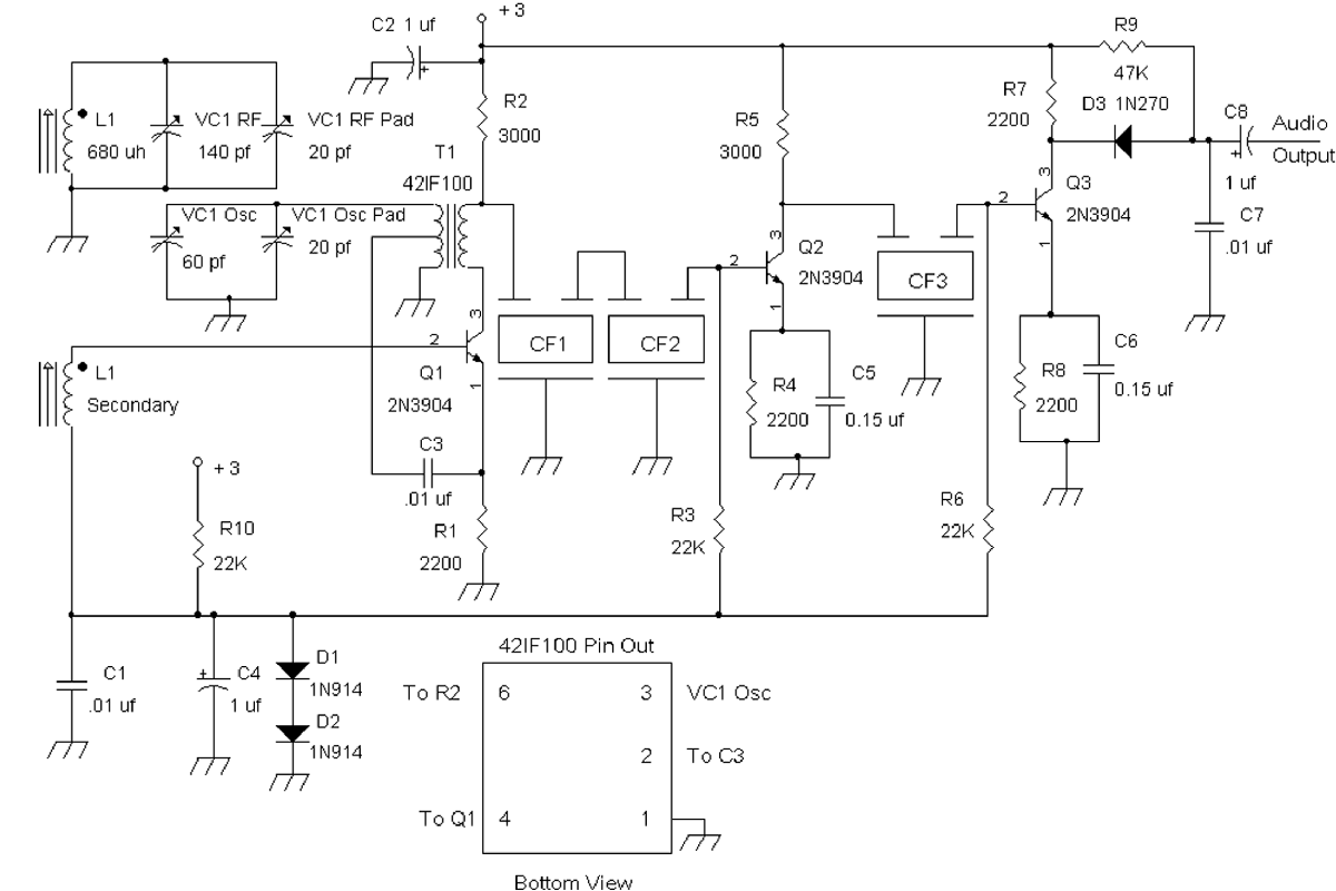
FIGURE 11-3 Schematic diagram of an AM radio with ceramic filters using a 3-volt supply.
Gyrators (aka Simulated or Active Inductors)
When generating FM was in its infancy, there were no varactor tuning diodes. The FM transmitter back in the 1930s or 1940s used vacuum tubes for amplification, for oscillation, and for modulation of the frequency of the oscillator. The choice circuit to generate FM of that era was the reactance modulator. The reactance modulator circuit consisted of a vacuum tube that acted as a variable inductor. With no audio signal into this vacuum tube, an inductance of fixed value was formed in parallel with the oscillator’s main coil. If the vacuum tube changed in plate current due to an audio signal, the inductance changed as well. So for a fixed plate current in the vacuum tube, a fixed inductor was synthesized from the plate to the cathode of the tube. Today, the reactance modulator can be designed with field-effect transistors, bipolar transistors, and/or integrated circuits.
For this book, we will be working with simulated inductors or gyrators consisting of solid-state devices, and the inductance will be fixed.
Figure 11-4 shows a very simple gyrator. The gyrator in the figure is a “simulated” inductor with one lead that is grounded. So looking into the C1 and R2 input terminal of the gyrator is equivalent to looking into a regular inductor as in the lower portion of the figure with the other lead grounded.
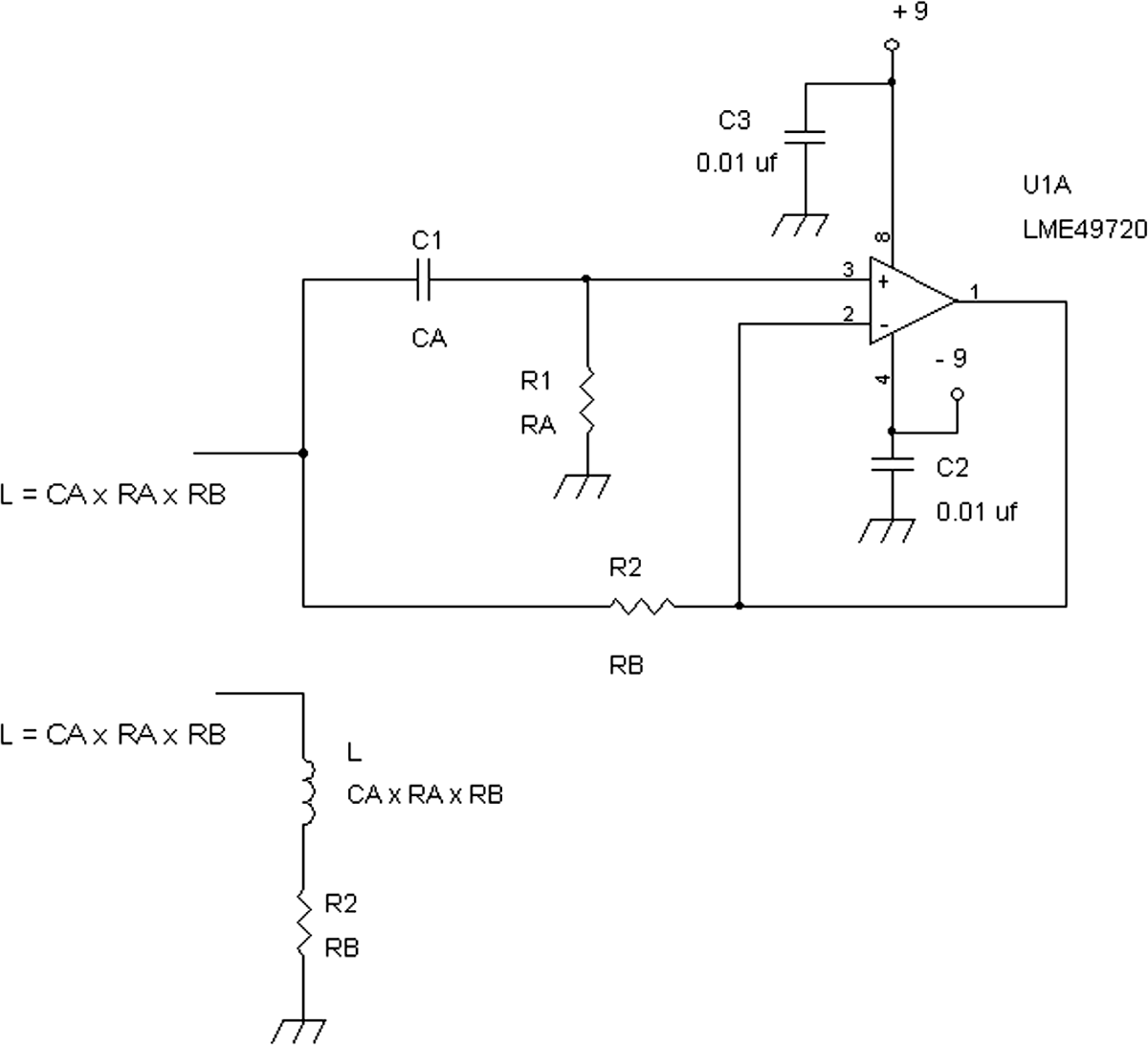
FIGURE 11-4 Gyrator using a gain-of-1 op amp voltage follower circuit.
An off-the-shelf inductor or coil always has at least two characteristics. The first is the inductance, and the other is the DC resistance. So any coil can be modeled as a perfect inductor with a series resistance. The lower the DC resistance of the coil, the closer this coil comes to an ideal inductor. At a low frequency or at DC, the impedance of the coil is just its internal resistance. For example, an antenna coil’s primary winding may be anywhere from 1 ![]() to 10
to 10 ![]() in terms of internal resistance. And at high frequencies, the coil has a very high impedance if there is no appreciable capacitance in the coil.
in terms of internal resistance. And at high frequencies, the coil has a very high impedance if there is no appreciable capacitance in the coil.
Now let’s look at Figure 11-4. The input of the gyrator circuit is C1 and R2. C1 and R1 form a high-pass filter network, which means that at low frequencies there is reduced amplitude or no low-frequency signals across R1. At high frequencies, C1 acts closer to a short circuit, which means that high-frequency signals appear at R1. The signal at R1 is amplified by a gain of 1 and fed back to the input via R2.
So let’s take a look at what happens if the signal at the input is a DC voltage. C1 will block the DC voltage, and the voltage at R1 will be zero. The output of the amplifier then will be zero as well, which grounds one end of R2. This means that at DC the input of the gyrator is just a resistor, R2. Note that a coil at DC is also just the internal resistance, which means that a coil can be modeled at DC as a resistor as well.
For a high-frequency signal at the input of the gyrator, C1 passes most or all of the input signal into R1. One can say that the high-frequency signal at the input and output of the amplifier is really close to or the same as the signal appearing at the input of the gyrator circuit. This then means that signal voltage on R2 that is connected to the amplifier is really about the same signal voltage at the input of the gyrator. But R2 is also connected to the input. If we assume that R1 is very large and does not load the input signal, then most or all of the signal current flowing to the gyrator is through R2. But, if the signal voltage on both ends of R2 is almost the same or is the same, then there is no net current flowing into R2. Recall Ohm’s law, which says that it is the potential difference (voltage difference) across a resistor that determines the current flowing into the resistor. If the voltage is the same on both ends of R2, then the potential difference is zero, and thus there is no current through R2. So, at high frequencies, there is little or no current flowing into R2 or the gyrator. At high frequencies the gyrator circuit looks like an open circuit or a very high impedance circuit.
But isn’t this the same as the effect on a coil at high frequencies? A high-frequency signal into a coil will measure as a very high-impedance device or as an open circuit. Thus the gyrator circuit is “equivalent” to a coil or inductor.
The gyrator circuit in Figure 11-4 has an inductance of L = C1 × R1 × R2. For example, if C1 = 1,000 pF, R1 = 1,000 ![]() , and R2 = 50
, and R2 = 50 ![]() (R2 is the equivalent internal resistance of a coil), then this gyrator has an inductance of 50 μH. However, in practice, the Q of this gyrator circuit usually does not exceed 10. Note that the Q values of antenna coils and IF transformers are at least 50 typically. So the gyrator circuit in Figure 11-4 is not quite suitable for an IF filter, for example.
(R2 is the equivalent internal resistance of a coil), then this gyrator has an inductance of 50 μH. However, in practice, the Q of this gyrator circuit usually does not exceed 10. Note that the Q values of antenna coils and IF transformers are at least 50 typically. So the gyrator circuit in Figure 11-4 is not quite suitable for an IF filter, for example.
But there is another type of gyrator circuit that has two amplifiers and works as a generalized impedance converter (GIC). Gyrators using a GIC topology generally have a Q of 50 or more. (Figure 11-6B shows a gyrator circuit using op amps U7A and U7B.)
Inductor-less (aka Coil-less) Superheterodyne Radio
Here is a problem to solve: How do you design a superheterodyne radio without any coils? One way is to substitute every inductor with a gyrator. Or if a band-pass filter is needed, one can use a ceramic filter or a gyrator.
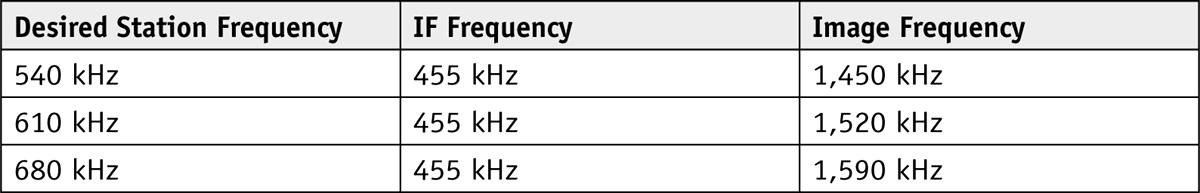
But what if you want to design an inductor-less superheterodyne radio with just a one-section variable capacitor or, better yet, tune the radio without a variable capacitor at all? So this was what I was thinking during the last four months before I was going to write this book. The initial design was to use ceramic filters for the IF stages and no tuned RF stage. This design would work, except that using a 455-kHz ceramic filter with a single conversion RF mixer circuit would result in receiving radio signals at image frequencies.
For example, without a variable band-pass filter tuned to the desired frequency and fed to the converter or mixer circuit, an image signal will convert (or mix down) to the same IF frequency at twice the IF frequency (e.g., twice the IF frequency = 2 × 455 kHz = 910 kHz) plus the frequency of the desired station. See the following table for some examples.
However, there is another technique called double conversion that eliminates receiving stations at the image frequencies. But a double-conversion radio requires a second mixer or converter circuit and other IF filters. The double-conversion radio is workable, but it was decided that the inductor-less radio design will stick to just one converter circuit instead.
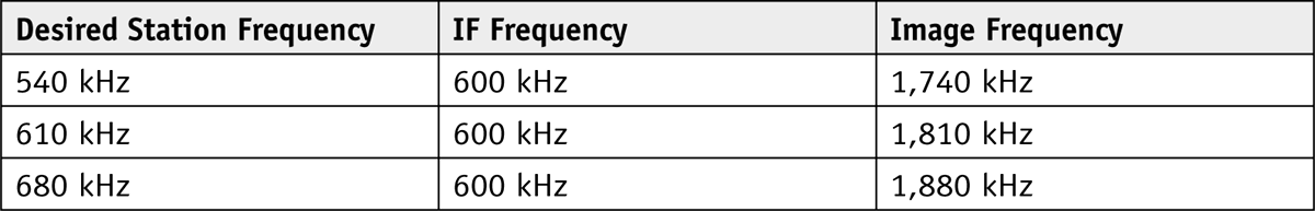
Therefore, to get around the problem of receiving stations at image frequencies, the IF frequency was raised to about 600 kHz (or higher), and a broadband low-pass filter was used to remove signals higher than 1,600 kHz. Any signal above 1,600 kHz would be filtered out and not able to mix or convert down to the new 600-kHz IF frequency. See the following table for some examples.
As stated previously, any signal above 1,600 kHz will be attenuated or removed by a low-pass filter. Figure 11-5 is a block diagram for an inductor-less superheterodyne radio. For the antenna, a short wire of less than 2 or 3 feet or a telescoping antenna will be sufficient to pick up radio stations in the AM broadcast band. The antenna is connected to a high-pass filter to attenuate signals below the AM band so that the radio minimizes picking up hum or other low-frequency signals. From the output of the high-pass filter, the wide-band RF signal is amplified by a low-noise circuit so that any noise contribution from the succeeding low-pass filter is negligible. The output of the low-noise amplifier is connected to the input of a 1.6-MHz low-pass filter, and the output of the low-pass filter is fed to a unity gain inverting amplifier and to an input of a balanced RF mixer. The output of the unity gain inverting amplifier is fed to the other input of the balanced RF mixer. A local oscillator formed by the same type of hysteresis oscillator circuit as shown in Chapter 4 provides twice the local oscillator frequency. The output of the local oscillator is connected to a flip-flop divide-by-two circuit that provides a “perfect” square wave at the local oscillator frequency signal to the balanced mixer.
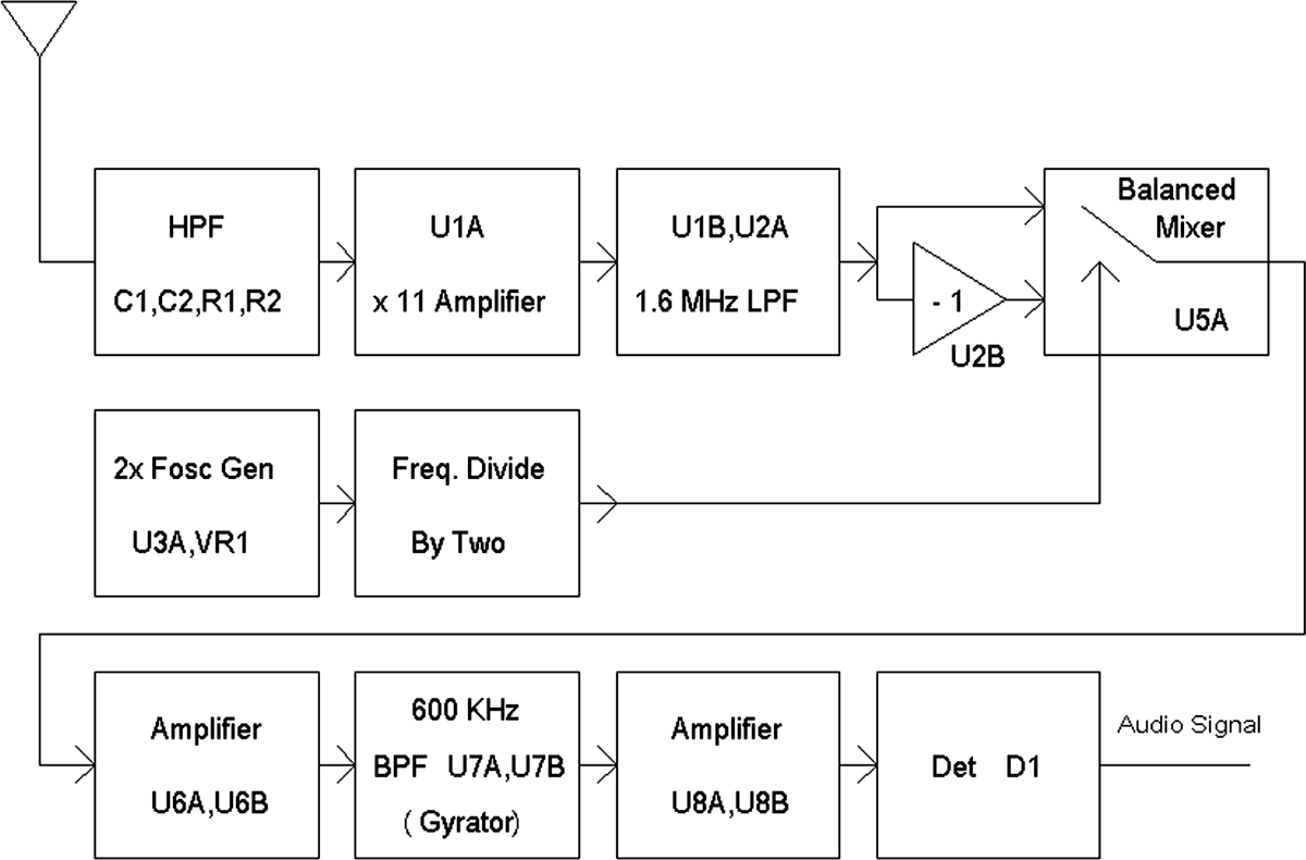
FIGURE 11-5 Block diagram of an inductor-less radio.
The mixer is balanced because neither the oscillator signal nor the RF signal from the low-pass filter appears at the output of the balanced mixer. Only a multiplied signal (RF signal times the oscillator signal) appears at the output. From the output of the balanced mixer, the sum and difference frequency signals are amplified and then fed to a single high-Q gyrator band-pass filter. The output of the 600-kHz IF band-pass filter is further amplified and then finally demodulated with a detector (e.g., diode envelope detector).
Parts List
• C1: 0.0056 μF
• C2: 0.0018 μF
• C3, C4, C27: 0.15 μF
• C5: 0.001 μF 5%
• C6: 0.0022 μF 5%
• C7: 100 pF 5%
• C8: 0.0027 μF 5%
• C10: 30 pF 5%
• C11, C12, C13, C14, C15, C17, C18, C24, C25, C28, C32, C33, C34: 0.01 μF
• C16, C22, C31: 100 μF, 16 volts
• C20: 24 pF 5% or 22 pF 5%
• C21, C26, C35, C36, C37, C38, C39: 1 μF, 35 volts
• C23: 47 pF 5%
• C29, C30: 510 pF 5%
• R1, R4: 100 ![]()
• R2, R6, R7, R8, R9, R10: 301 ![]() 1%
1%
• R3, R13, R14, R15, R16, R34: 10 k![]()
• R5, R11, R12, R20, R22, R30, R31: 1,000 ![]() 1%
1%
• R17: 910 ![]() or 820
or 820 ![]()
• R18: 2,000 ![]()
• R19: 47 k![]()
• R21, R23, R29, R32: 3,900 ![]()
• R24, R33: 100 k![]()
• R25, R26, R27, R28: 511 ![]() 1%
1%
• U1, U2, U7: LME49720 or LM4562
• U3: 74AHC14 or 74HC14
• U4: 74HC74 or 74HCT74
• U5: 74HC4053
• U6, U8: NE5532 or LM833
• U9: LM78L05 or LM7805
• VR1: 1-k![]() pot
pot
• VR2: 10-k![]() pot
pot
• D1: 1N270 or 1N34 or 1N914
Figures 11-6A and 11-6B provide schematic diagrams for the inductor-less radio. A short wire or telescopic antenna is connected to a high-pass filter circuit consisting of R1, R2, C1, and C2, which has a cutoff frequency at about 280 kHz. This high-pass filter removes or attenuates low-frequency signals that would be demodulated as hum or extraneous noise. The output of the high-pass filter at C2 then is coupled to a five-pole 1,600-kHz active low-pass filter consisting of capacitors from C5 to C10, U1B, and U2A. The output of the low-pass filter is inverted in phase via U2B so that the inputs of the mixer U5A have a balanced or push-pull signal. Thus the inputs of the balanced mixer U5A are connected to a noninverting output of the low-pass filter and an inverting output of the low-pass filter. By commutating between the noninverting and inverting outputs of the low-pass filter, multiplication occurs with the local oscillator signal from the flip-flop frequency divider circuit U4A.
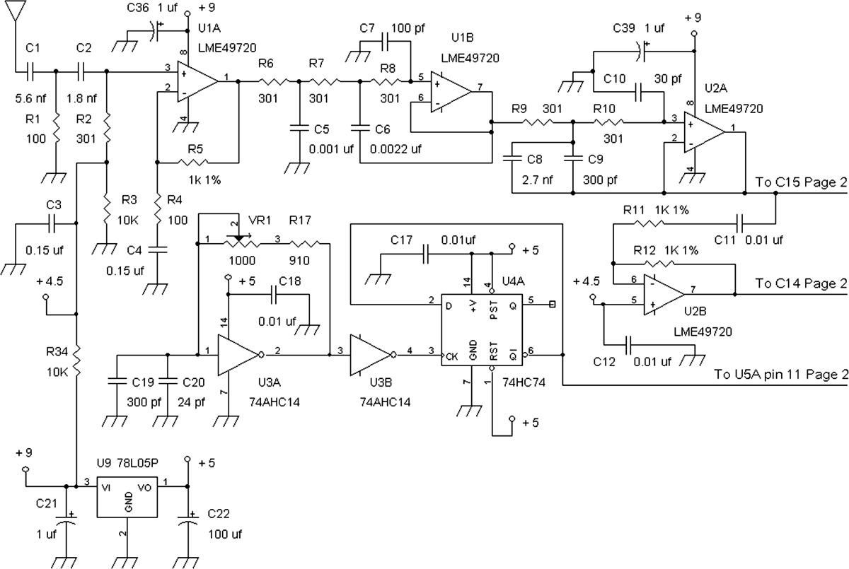
FIGURE 11-6A Inductor-less radio schematic diagram part 1—amplifiers and mixer.

FIGURE 11-6B Inductor-less radio schematic diagram part 2—gyrator, amplifiers, and detector.
The local oscillator signal is generated by a hysteresis oscillator circuit much like the one seen in Chapter 4, which was used as an RF generator. Since the hysteresis oscillator in Chapter 4 is sufficiently stable in frequency for generating an RF signal to test a radio, it is also stable enough to be used as a local oscillator in this inductor-less receiver.
With an IF frequency set at 600 kHz, the desired local oscillator signal’s frequency to the balanced mixer is 540 kHz 1 600 kHz to 1,600 kHz 1 600 kHz, or 1,140 kHz to 2,200 kHz. The hysteresis oscillator U3A must generate twice the frequency because a divide-by-two circuit, U4A, halves the frequency of the oscillator. Therefore, the output signal frequency of U3A must be adjustable via VR1 to range from 2,280 kHz to 4,400 kHz.
You may ask why not skip the divide-by-two circuit and connect U3A directly to the mixer U5A. It turns out that by dividing the oscillator’s frequency by two via U4A, a perfect square wave is used as the commutating signal for mixer U5A. The square wave is symmetric, which then allows the mixing or multiplying effect to be balanced such that the RF signal from the low-pass filter does not appear at the output of U5A. The hysteresis oscillator does not generate a perfectly symmetric waveform. That is, the logic high duration is not equal to the logic low duration. Sending such a nonsymmetric waveform to the mixer will cause leakage of the RF signal to the output of the mixer, which is not preferred in a balanced-mixer configuration.
in Chapter 10 concerning the one-transistor superheterodyne radio, it was mentioned that having a huge-amplitude local oscillator signal added to the IF signal hampers proper envelope detection of the IF signal. And thus multiple IF filters are needed to sufficiently remove or attenuate the oscillator signal.
In this inductor-less radio, there is only one IF filter, so great care must be taken at the design stage to provide a mixer/converter circuit that outputs essentially no local oscillator signal nor the RF signal. This is the reason for using a balanced mixer.
The output of the balanced mixer is fed to a second low-pass filter at around 1,600 kHz to remove the very high-frequency components from the balanced mixer owing to the square-wave switching. The output of this second low-pass filter is fed to amplifiers U6A and U6B. VR2 serves as a variable gain control to adjust the IF gain. The output signal from U6B then is band-pass-filtered via R24, resonating capacitor C29, and gyrator (active inductor) circuit U7A and U7B that has an inductance of [(C30 × R28 × R25 × R27)/R26] = L. R24 sets the Q of the parallel tank circuit to greater than 50 at a resonant frequency of 600 kHz. The 600-kHz IF signal from the output of the band-pass circuit is further amplified via U8A and U8B before being demodulated by D1. Audio signals via C35 then are connected to a crystal earphone or to an audio amplifier. Also, a power switch may be connected in series with the battery or power source to conserve energy.
Note that the inductor-less superheterodyne radio is simple to use. There are no coils to adjust, and there are no multiple-gang variable capacitors to deal with. And this radio uses very common parts that are more available than the antenna coils, IF transformers, ceramic filters, and/or variable capacitors that were used in previous superheterodyne radio designs.