Chapter 23
Learning by Doing
In the last 10 chapters, Chapters 13 through 22, quite a lot of math was involved in explaining how signals and circuits work. However, for this last chapter, I will return to a more “hands-on” approach with experimentation with simple circuits. Before these elementary circuits are explored, I will revisit two previous circuits, the one-transistor superheterodyne radio and the software-defined radio (SDR) front-end circuit.
Therefore, the objectives of this chapter are
1. To show an updated improvement to the one-transistor radio
2. To comment on the 40-meter-band SDR front-end cicuit
3. To experiment with mixers and using Spectran, a free spectrum analyzer software program for the personal computer (PC)
4. To run experiments on op amps and current sources
5. To observe how an LC circuit works
6. To learn the Thevenin equivalent circuit
7. To analyze a bridge circuit
8. To give my thoughts on electronics, writing this book, and learning
The test equipment required in this chapter includes two signal generators with adjustable amplitude. The frequency range of one of the generators should provide up to a 1-MHz sine-wave signal. Also, a dual-trace oscilloscope of 10-MHz bandwidth or more is required. A four-trace scope is preferred.
Update on the One-Transistor Superheterodyne Radio
The first version of the one-transistor superheterodyne radio had a few drawbacks; most notably, it had insufficient volume (Figure 23-1). The original one-transistor schematic diagram is shown as Figure 23-1.
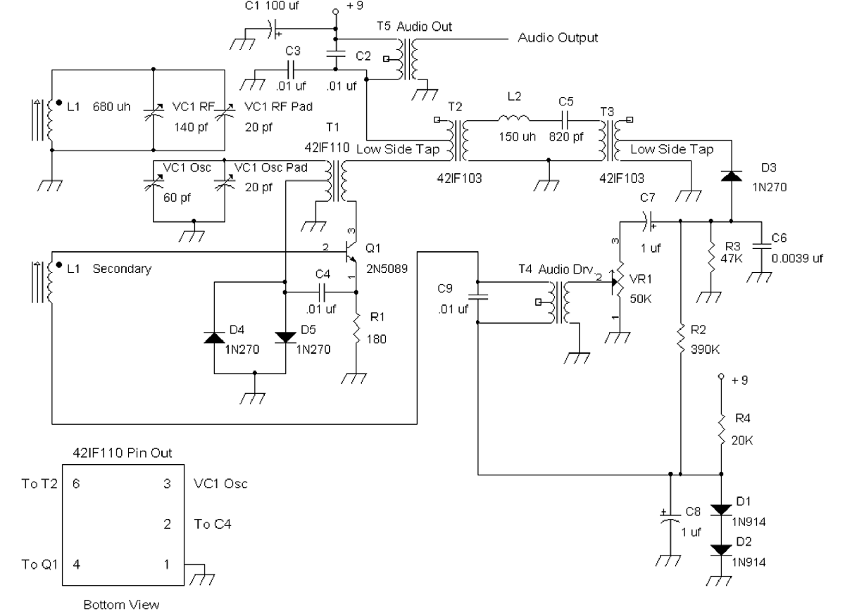
FIGURE 23-1 Original one-transistor radio design.
In Figure 23-1, the audio signal from the audio driver transformer T4 is fairly small. The emitter resistor R1 reduces the transconductance of Q1, thereby reducing the audio gain. When C4 was increased to a larger capacitance, such as 1,000 μF, to increase the audio gain by using the tapped winding of T1 to ground the emitter, squegging resulted. Squegging is a condition where an oscillator’s signal turns on and off at a low frequency rate and is caused by the large coupling capacitors in the signal path.
One possible solution is to replace R1 with an inductor with a value of 470 μH to 1,000 μH; at audio frequencies, the impedance of the inductor is the direct-current (DC) coil resistance, and at the oscillator frequency, the impedance of the inductor is high. The resistance of these inductors typically will run about = to 10 ![]() , and therefore, one has to measure the resistance of the inductor first before replacing R1. The DC bias line to the base of Q1 via C8 will have to be removed because it now requires a variable bias voltage to set a new bias voltage to the base of Q1 such that the emitter voltage divided by the (470-μH) coil resistance is about 10 to 20 mA.
, and therefore, one has to measure the resistance of the inductor first before replacing R1. The DC bias line to the base of Q1 via C8 will have to be removed because it now requires a variable bias voltage to set a new bias voltage to the base of Q1 such that the emitter voltage divided by the (470-μH) coil resistance is about 10 to 20 mA.
In Figure 23-2, the collector current of Q1 is set by VR2. The coil resistance of L3 is measured, and VR2 is varied until the emitter voltage across the coil resistance results in an emitter current of about 15 mA.
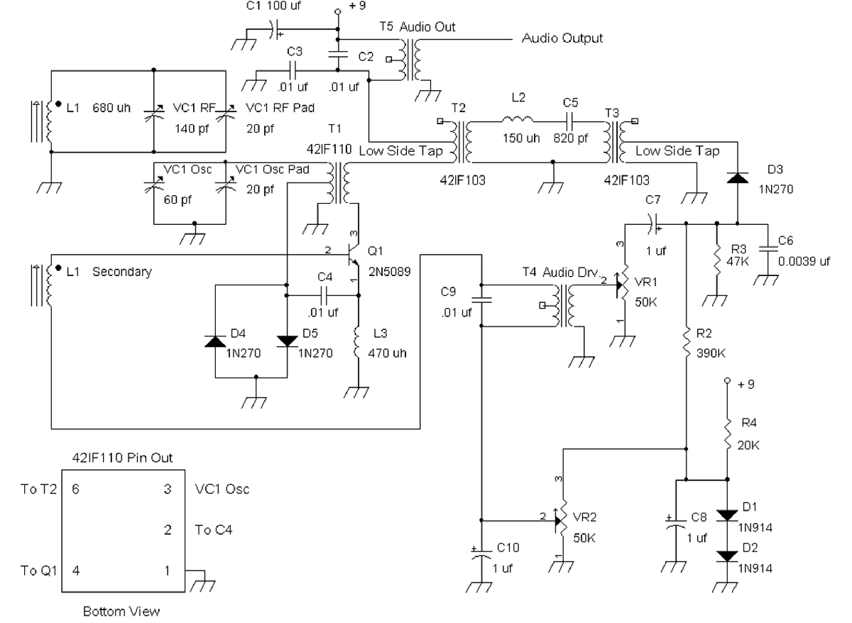
FIGURE 23-2 One-transistor radio with a “possible” modification for higher audio volume.
Alternatively, see Figure 23-3, a modified schematic with changes in the oscillator configuration and the IF filter, T2, T6, and T3.
In Figure 23-3 the emitter resistor R1 is reduced dramatically from the previous design from 180 ![]() to 5.1
to 5.1 ![]() . This reduction allows for higher audio gain to provide a sufficient loudness from a speaker. Although T5 has a primary impedance of 1,000
. This reduction allows for higher audio gain to provide a sufficient loudness from a speaker. Although T5 has a primary impedance of 1,000 ![]() and 8
and 8 ![]() for the secondary, it was found that replacing T5 with a 500-
for the secondary, it was found that replacing T5 with a 500-![]() primary impedance and an 8-
primary impedance and an 8-![]() secondary impedance rating allowed for a higher audio level.
secondary impedance rating allowed for a higher audio level.
FIGURE 23-3 One-transistor superheterodyne radio version 2.0.
The adjustment for VR2, the bias control, requires some care. After the initial adjustment of VR2, the transistor warms up. As the transistor warms up, the collector current changes. This collector-current change then causes the oscillator’s frequency to shift somewhat. Therefore, VR2 may need readjustment. VR2 is set to provide 0.070 volt DC at the emitter of Q1. Then, with an oscilloscope, measure the oscillator signal at the base of Q1 for 200-mV peak-to-peak amplitude by adjusting VR3.
![]()
Please note that the oscillator circuit in Figure 23-3 is different from the circuits shown in Figures 23-1 and 23-2. Therefore, notice that pins 4 and 6 are reversed in oscillator coil T1 (42IF110). See the notes in Figure 23-3.
Comments on SDR 40-Meter Front-End Circuit
In Chapter 12, the front-end circuit from Figure 12-11B proved satisfactory for receiving amateur radio signals on the 40-meter band. The figure is shown again in Figure 23-4.
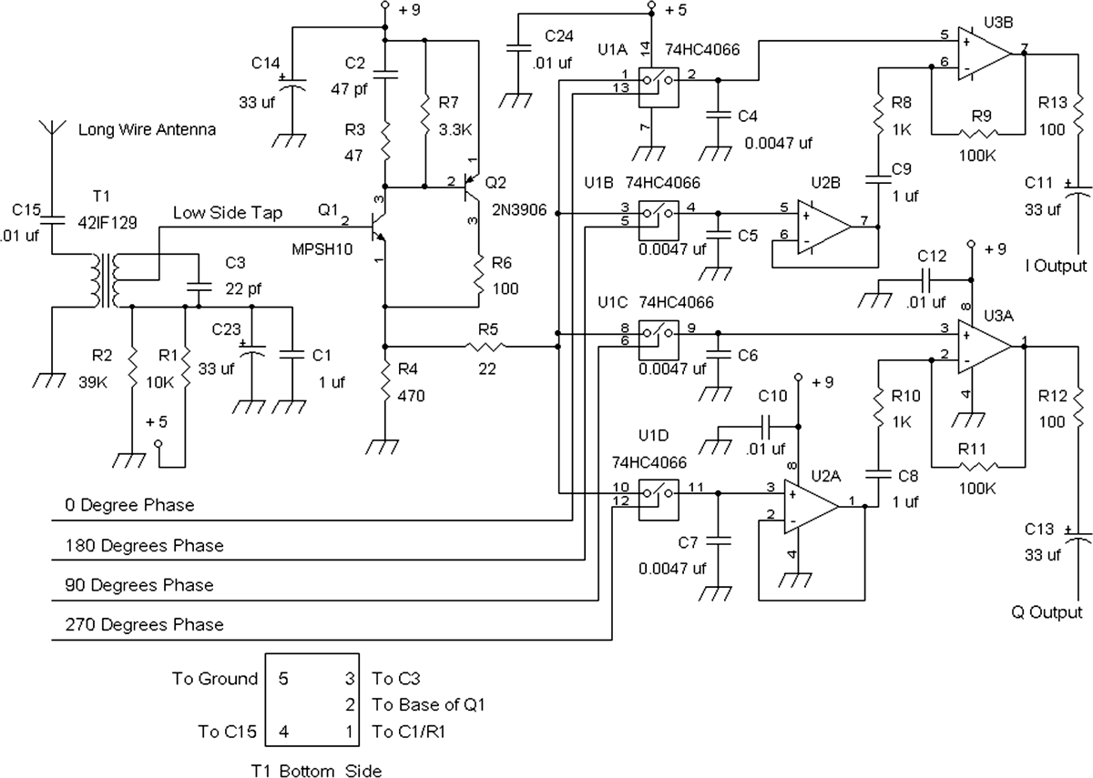
FIGURE 23-4 A 40-meter band front-end circuit.
This front-end circuit supplied the I and Q low-frequency IF signals to a 192-kHz sampling-rate sound card and then was compared against a Yaesu FT-707 high-frequency (HF) band receiver. The FT-707 was better overall, but this front-end circuit managed to pull in some weak stations fine with a 25-foot-long wire antenna. If I had to redesign the circuit, I would make one small change. I would replace the bipolar transistor Q1, an MPSH10, with a low-noise junction field effect transistor (JFET), such as a 2SK152 or a J110, to reduce noise further, but the input biasing circuits consisting of R1, R2, R7, and R4 would have to be changed. By using a JFET, input bias noise current is not a problem compared with a bipolar transistor. Thus the radio-frequency (RF) transformer T1 can be configured to provide a higher signal level from the high-side tap (instead of signal from the low-side tap) to the gate of the JFET. Other ways to reduce noise would involve replacing the op amps with ultralow-noise types (<1 nV/![]() ) or replacing Q1 and Q2 with a voltage-gain stage. However, these changes may not be worth the trouble because it is always easier to use a better antenna, which would overcome the noise caused by the front-end circuit. One of my amateur radio friends told me that when a good 40-meter antenna is connected to the receiver, the atmospheric (electrical) noise dominates over any noise caused by the front-end circuits, or alternatively, he recommends a digital signal processing (DSP) audio filter from AM-COM, Inc., that reduces hiss by at least 3- to 10-fold voltage-wise (10 dB to 20 dB).
) or replacing Q1 and Q2 with a voltage-gain stage. However, these changes may not be worth the trouble because it is always easier to use a better antenna, which would overcome the noise caused by the front-end circuit. One of my amateur radio friends told me that when a good 40-meter antenna is connected to the receiver, the atmospheric (electrical) noise dominates over any noise caused by the front-end circuits, or alternatively, he recommends a digital signal processing (DSP) audio filter from AM-COM, Inc., that reduces hiss by at least 3- to 10-fold voltage-wise (10 dB to 20 dB).
Experimenting with Mixers and Using the Spectran Spectrum Analyzer Program
An audio spectrum analyzer used to cost $5,000 twenty or thirty years ago. However, today one can obtain an audio spectrum analyzer with a computer and a free program, Spectran. The minimum sampling rate for most sound cards today is at least 48,000 samples per second, which allows processing audio signals up to about 24 kHz.
A doubly balanced mixer is a mixer that ideally provides only the product of the two input signals, without the passage of either or both input signals to the output of the mixer. We can use Spectran to observe the performance of a doubly balanced mixer, as shown in Figure 23-5.
FIGURE 23-5 A doubly balanced mixer for spectrum analysis.
To ensure that the input signal is not leaked through into the output, the commutating switcher U1 is provided with a square-wave switching signal (50 percent duty cycle) via binary divider U3. And to ensure that the square-wave switching signal is not leaked through to the output, the DC bias points are identical at both inputs of the analog switch U1A and there is also equal amplitude but opposite phases of the input signal provided to the inputs of U1A. Phase-splitter circuit Q1 provides nearly equal amplitude and opposite phases when R3 and R4 are identical in value (e.g., 1 percent or better tolerance resistors) and when the β of Q1 is high (>100). In practice, R4 is typically 1 percent larger in value than R3, or R3 is 1 percent smaller in value than R4. For R4 = 475 ![]() , the preferred resistance value is about 480
, the preferred resistance value is about 480 ![]() , whereas R3 = 475
, whereas R3 = 475 ![]() .
.
The supply voltage is at 4.5 volts to 6 volts DC to avoid overvoltage on the logic chips and analog switch. With the components R11 and C8 selected, the output of pin 9 of U3 (74HC74) is a square wave of = kHz. The input terminal provides a 4-kHz sine-wave signal of about 0.5 volt peak to peak. Couple the output of the mixer circuit via R10 to the left or right channel of the computer’s sound card line input. If a microphone input is used, a lower-amplitude signal from the mixer can be taken from the microphone level output terminal, where R13 and R14 are connected.
Download the Spectran program from the Web via http://digilander.libero.it/i2phd/spectran.html. The version 2 spectrum analyzer file is about 600 kB, and there is a 252-kB PDF operating manual that also can be downloaded. See Figure 23-6 for a sample Spectran display. Click on “Show Controls” to select the sampling frequency and resolution, as shown in Figure 23-7.
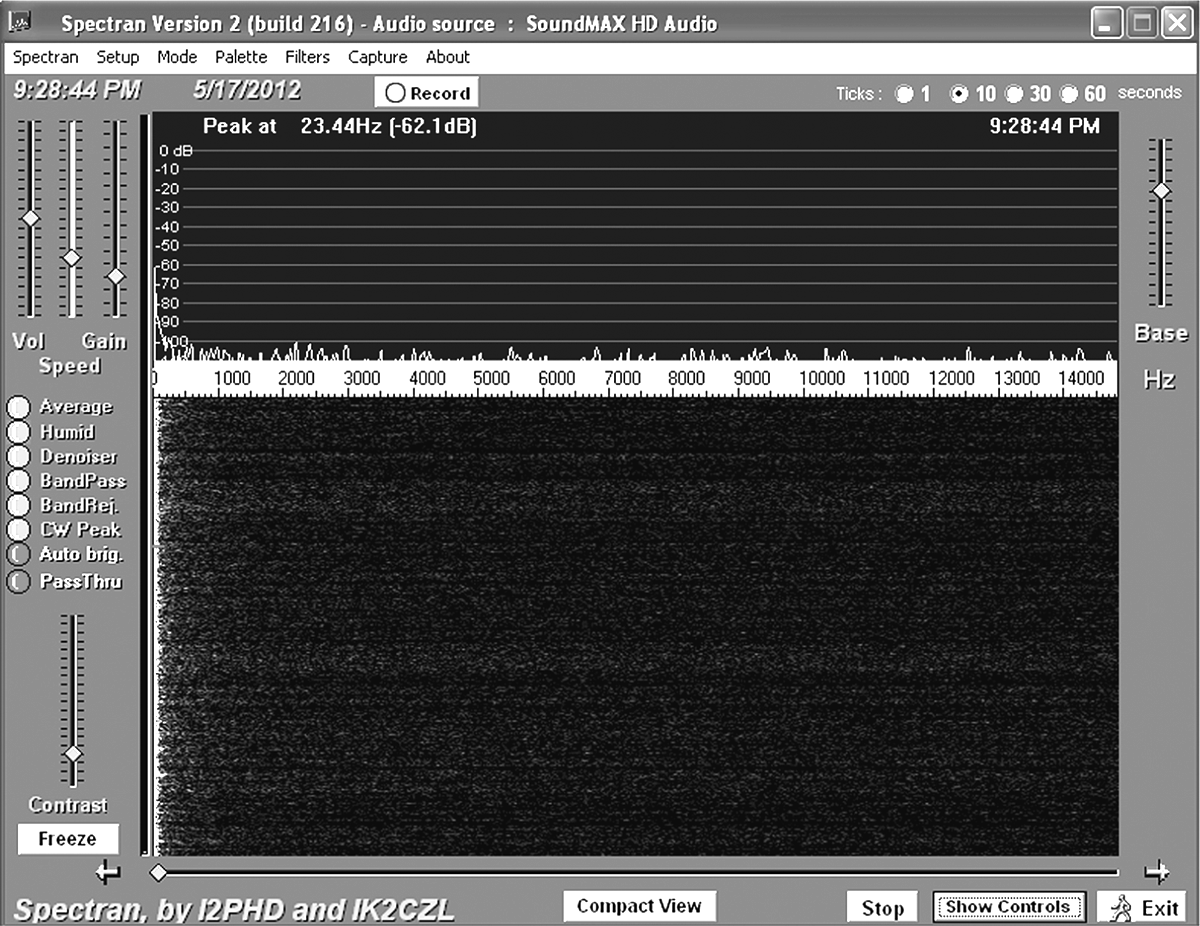
FIGURE 23-6 A sample Spectran display.

FIGURE 23-7 Selection of sampling frequency and bin width.
The sampling rate of 48 kHz is checked because this sampling rate should be available to all sound cards using the Window XP operating system. A resolution of 23 Hz is chosen such that a span from 0 Hz to almost 15 kHz is available without having to use the frequency-offset slider control ← and →. A finer resolution such as 12 Hz can be chosen, but the span will be cut in half to about 7.5 kHz of bandwidth, and the frequency-offset slider control must be used. See Figure 23-8.
Figure 23-8 shows the frequency-offset slider control displaying a span of frequencies from about 5,800 Hz to about 13,100 Hz.
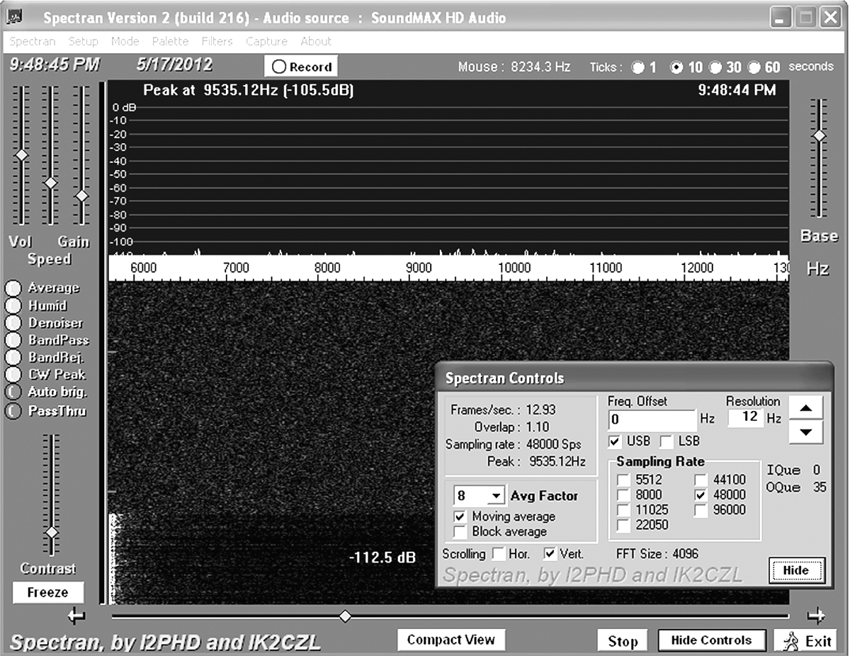
FIGURE 23-8 Using the frequency-offset slider control on a finer resolution mode.
With a 4-kHz sine-wave signal of about 0.5 volt peak to peak (0.25 volt peak) at the input, the spectrum of the doubly balanced mixer typically should have a spectrum displayed as shown in Figure 23-9. Figure 23-9 shows that the switching signal at about 5.2 kHz and the input signal at 4 kHz are suppressed by at least 40 dB or to 1 percent of the output signals whose frequencies are at 1.2 kHz (e.g., an IF signal or difference-frequency signal) and at 9.2 kHz, the summed frequency signal.
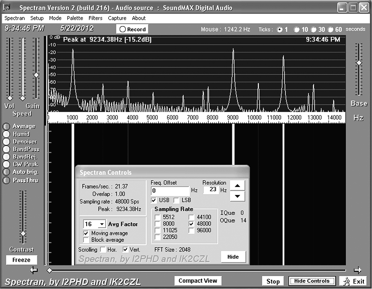
FIGURE 23-9 Output spectrum for a 4-kHz input signal.
Also observe that there is mixing action around 15 kHz by using the frequency-offset slider control (Figure 23-10). Figure 23-10 shows harmonic mixing at around 15.6 kHz, the third harmonic of the 5.2-kHz switching signal. The difference frequency is 15.6 kHz – 4 kHz = 11.6 kHz, and the sum-frequency component is at 15.6 kHz 1 4 kHz = 19.6 kHz.

FIGURE 23-10 Harmonic mixing at around 15.6 kHz.
Spectran is also great for analyzing the Fourier transform of pulse waveforms. For example, in Chapter 15, a pulse of 25 percent duty cycle produced frequencies at the fundamental frequency plus all multiples of harmonics except every fourth harmonic (e.g., fourth, eighth, etc.). Figure 23-11 provides a spectrum of a 25 percent duty-cycle pulse for a 1-kHz signal with a 250-μs pulse, a 1,000-μs period, and 0.380 volt peak-to-peak amplitude (into the line input of a sound card).
In Figure 23-11, the spectrum of a 1-kHz 25 percent duty-cycle pulse signal shows frequency components at all frequencies with every fourth harmonic nulled. Thus signals at 4 kHz, 8 kHz, and 12 kHz and so on are reduced substantially in amplitude. The 1-kHz 25 percent duty-cycle pulse waveform was provided by a function generator with a duty-cycle adjustment. Alternatively, one can use a counter and logic gates to provide the 25 percent duty-cycle waveform, as shown in Chapter 12 with the 40-meter-band SDR front-end circuit.
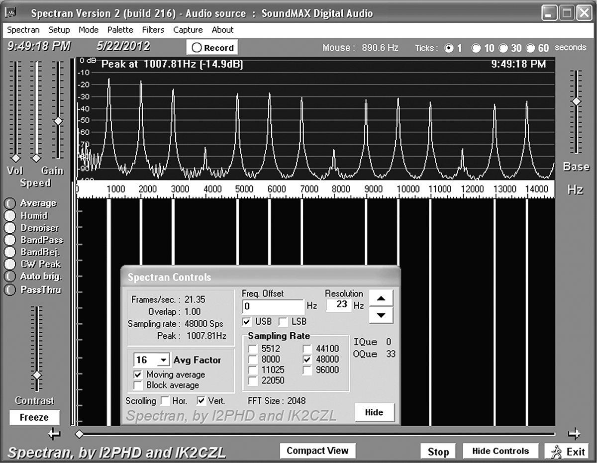
FIGURE 23-11 Spectrum analysis via Spectran of a 25 percent duty-cycle pulse-train waveform.
Now we will turn to a basic one-transistor mixer, as shown in Figure 23-12. The figure looks more like a common-emitter or grounded-emitter amplifier, which is for small signals at the base of less than 10 mV peak to peak. However, when a large sinusoidal signal of more than 200 mV peak to peak is combined with a small signal of a different frequency, a mixing or multiplying effect occurs.
Look at Figure 23-12. At the base of Q1, resistors R1 and R3 attenuate the input signal Vin1 by 100-fold, and resistors R2 and R3 attenuate the input signal Vin2 by 11-fold. With a sine-wave generator at 11 kHz with 4 volts peak of amplitude connected to input terminal Vin2 of the mixer, connect a 1-volt peak-to-peak sine-wave signal at 6.5 kHz into input terminal Vin1. Now connect the output of the mixer via R8 or R9/R10 to the sound card of the computer with the Spectran program running. Observe that there is a difference-frequency signal of 4.5 kHz (an IF signal) and that its amplitude is almost the same as the 6.5-kHz signal at the output of the mixer. This “equality” in amplitude level confirms that when a large-amplitude sinusoidal signal of a first frequency is combined with a small-amplitude signal of a second frequency, the output of the mixer provides that intermodulation distortion signal, which is the IF signal at about the same amplitude as the amplified small-amplitude signal of the second frequency. And this “equality” in amplitude level confirms that the conversion transconductance of a bipolar mixer is just the same as the small-signal transconductance when a large-amplitude signal is involved (see Figure 23-13).
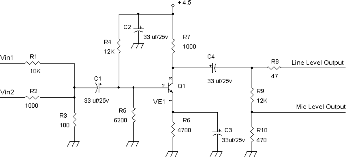
FIGURE 23-12 A one-transistor mixer that is typically used in radios.
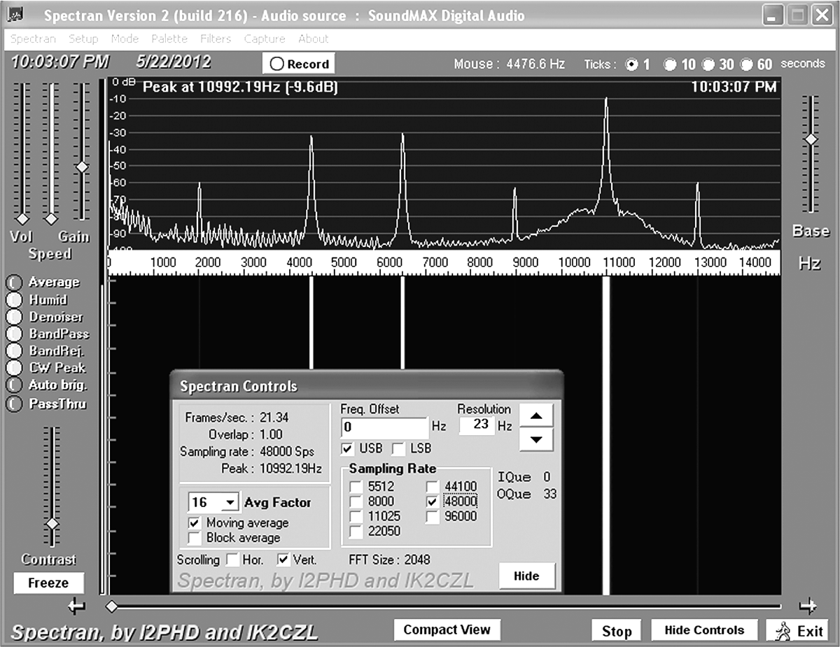
FIGURE 23-13 Spectrum of the one-transistor mixer via Spectran.
Lowering the large-amplitude 11 kHz signal will lower the conversion transconductance and thus lower the intermodulation distortion signal at 4.5 kHz.
In Figure 23-13, note at the output of the mixer that the IF signal at about 4.5 kHz has roughly the same amplitude as the input signal at 6.5 kHz. This confirms that a large oscillator voltage of greater than 200 mV peak to peak into the base emitter junction of a mixer transistor provides a conversion gain roughly equal to the small-signal gain.
With the 11-kHz signal removed and disconnected from the input terminal V_in2, one can confirm that second-harmonic distortion is about 1 percent per 1-mV peak sine wave. Therefore, a 1-![]() peak-to-peak 6.5-kHz sine-wave signal at V_in1 provides about 10 mV peak to peak or = mV peak sine wave into the base of Q1. Thus the second-harmonic distortion signal at 13-kHz should be about = percent (–26 dB) of the fundamental-frequency signal at 6.5 kHz. Spectran should confirm that the second harmonic is then about 26 dB down from the fundamental-frequency signal (see Figure 23-14).
peak-to-peak 6.5-kHz sine-wave signal at V_in1 provides about 10 mV peak to peak or = mV peak sine wave into the base of Q1. Thus the second-harmonic distortion signal at 13-kHz should be about = percent (–26 dB) of the fundamental-frequency signal at 6.5 kHz. Spectran should confirm that the second harmonic is then about 26 dB down from the fundamental-frequency signal (see Figure 23-14).
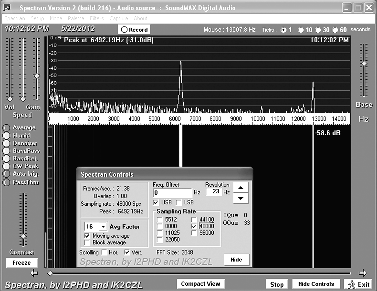
FIGURE 23-14 Spectrum of second-harmonic distortion via Spectran.
As seen in Figure 23-14, with the fundamental-frequency 6.5-kHz signal at -31.0 dB, the second-harmonic signal at 13 kHz is at -58.6 dB, which is about 27.6 dB lower than the fundamental-frequency signal. The calculated second harmonic is about 26 dB, so theory and practice match up well. Also note that the cable length of the audio cable to the sound card should be 3 feet or less if possible. The preceding measurement was done with a 15-foot-long cable, whose capacitance slightly rolls off the frequency response at about 13 kHz.
Another experiment one can try is to connect a series 200-![]() variable resistor to C3 such that the local feedback can be controlled at the emitter of Q1. By noting the emitter voltage VE1 and dividing it by the emitter resistor R6 = 4,700
variable resistor to C3 such that the local feedback can be controlled at the emitter of Q1. By noting the emitter voltage VE1 and dividing it by the emitter resistor R6 = 4,700 ![]() , the collector current is known. Then find the transconductance ICQ/0.026 volt, and set the series variable resistor to (½) × 0.026 volt/Icq to observe whether the third-harmonic distortion is nulled or minimized.
, the collector current is known. Then find the transconductance ICQ/0.026 volt, and set the series variable resistor to (½) × 0.026 volt/Icq to observe whether the third-harmonic distortion is nulled or minimized.
![]()
One can test harmonic and intermodulation distortion of audio devices (e.g., high-fidelity receivers and amplifiers) via Spectran.
Oh, just one more thing (as Lieutenant Columbo would say), the common-emitter amplifier shown in Figure 23-12 generates lots of distortion and is not usually used in practice for providing high-quality audio signal amplification. This type of amplifier is commonly shown in beginning electronic circuits classes, but what the textbook or the instructor does not tell the student is that the grounded-emitter amplifier distorts heavily with normal line-level audio signals (e.g., 100 mV RMS). In order to improve the distortion performance of this amplifier, some type of negative feedback is required.
Conducting Experiments on Op Amps and Amplifiers
This section explores frequency response of operational amplifier circuits. In Chapter 19 it was shown that a multiple-channel input linear mixing amplifier results in lower bandwidth than expected. Again, by linear mixing, I refer to additive mixing (e.g., Figure 23-15) instead of multiplicative mixing in RF circuits.
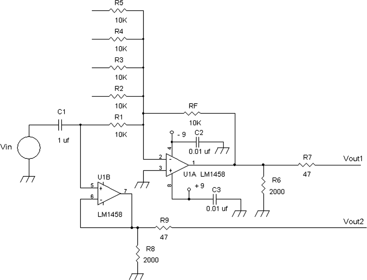
FIGURE 23-15 A five-input mixer and a voltage follower circuit with four unused input resistors floating.
With about a 1-volt peak-to-peak sine-wave signal, measure the frequency response of the inverting gain (–1) amplifier at Vout1 and the voltage follower amplifier at Vout2. The –3-dB bandwidth happens when the 1-![]() peak-to-peak signal drops to 0.707 volt peak to peak. Typically, the –3-dB bandwidth of an LM1458 for a unity-gain follower via Vout2 is about 1 MHz and 500 kHz at Vout1, where resistors R2, R3, R4, and R5 are not connected to ground yet. The inverting amplifier configuration for a gain of –1 should have half the bandwidth of the voltage follower.
peak-to-peak signal drops to 0.707 volt peak to peak. Typically, the –3-dB bandwidth of an LM1458 for a unity-gain follower via Vout2 is about 1 MHz and 500 kHz at Vout1, where resistors R2, R3, R4, and R5 are not connected to ground yet. The inverting amplifier configuration for a gain of –1 should have half the bandwidth of the voltage follower.
Now short resistors R2, R3, R4, and R5 to ground and remeasure the bandwidth at Vout1, which should be about one-third the previous measurement, or about 166 kHz (see Figure 23-16). Thus one needs to be careful in terms of bandwidth reduction caused by a multiple-input summing amplifier, as shown in Figure 23-15. When more inputs are added, the bandwidth shrinks further.
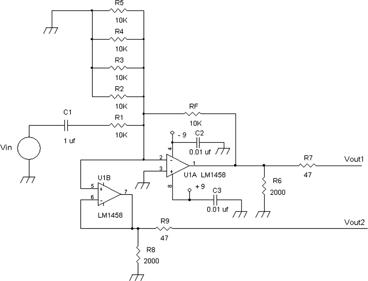
FIGURE 23-16 Unused inputs tied to ground for remeasurement of frequency response at Vout1.
Recall that the –3-dB response is given by bandwidth GBWP[Rpar/(RF 1 Rpar)], where Rpar is the parallel combination of all input resistors, and GBWP is usually the unity-gain bandwidth of the op amp.
We now turn to observing how an op amp provides flat frequency response for closed-loop gains set by the feedback resistors. An op amp in general without any negative feedback has an open-loop bandwidth of less than 1 kHz and typically less than 100 Hz. The question one would ask is: How does feedback provide a flat frequency response beyond the open-loop bandwidth?
To uncover this “mystery,” one way to find out is to build the circuit as seen in Figure 23-17. Figure 23-17 shows an inverting amplifier set for a gain of about –100. To prevent overloading the output, the input signal is attenuated by 10-fold such that a 1-kHz, 1-volt peak-to-peak sinusoidal waveform at input resistor R7 produces a 10-volts peak-to-peak signal at Vout1. The error signal Verror U1A at pin 2 of U1 (LM1458) is amplified by about 100 times via U2, a wider bandwidth op amp (a TL082). The (1) terminal of the LM1458 is grounded to provide a convenient way to measure the differential voltage across the (–) and (1) inputs of the 1458 op amp.
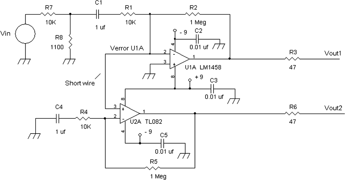
FIGURE 23-17 Analyzing the frequency response of the input terminal of an op amp.
Take a look at Figure 23-17. The experiment is as follows: Confirm that a 10-volt peak-to-peak signal appears at Vout1 at frequencies from 100 Hz to 5,000 Hz. The response at Vout1 should be flat from 100 Hz to 5,000 Hz with a small drop-off at 5,000 Hz. However, the frequency response at Vout2 should show a rising amplitude as frequency is increased (see Figure 23-18). Vout2 represents an amplified version of of the error signal across the (–) and (1) inputs of U1A, an LM1458 op amp, in Figure 23-17. Note that the (1) input of U1A is grounded.
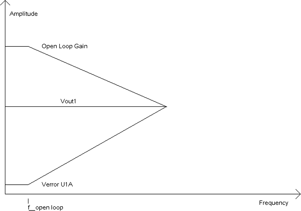
FIGURE 23-18 Frequency response at open loop and at the (–) input terminal.
If the error signal at the (–) terminal of the LM1458 has a flat frequency response, then the output signal at the LM1458 will have a rolled-off response at the open-loop bandwidth frequency such as 10 Hz. At 10 Hz, the gain is 0.707 of the gain at DC or at 1 Hz. The gain falls off after 10 Hz at approximately 10 Hz/f, where f 10 Hz. For example, at 100 Hz, the gain is one-tenth the gain at 1 Hz. At 1,000 Hz, the gain is one-hundredth or 1 percent of the gain at 1 Hz. Therefore, to provide a flat frequency response beyond 10 Hz, the error signal at the (–) input of the LM1458 must be increasing in a complementary manner or at approximately the reciprocal of the fall off response. Thus, at the (–) terminal of U1A, it has a response of about f /10 Hz. For example, the signal at 100 Hz at the (–) input terminal of the LM1458 must be 10 times higher than at 1 Hz.
This makes sense in that the open-loop frequency response has the characteristic of an integrator, and the frequency response at the (–) input terminal must have the characteristics of a differentiator. When a signal is integrated and then differentiated, or vice versa, the frequency response is flat.
So the next question is, is there a limit as to how high in frequency the input signal can go before something else happens at the (–) input? The answer is that there is a high-frequency limit if the output wants to maintain a flat frequency response. What happens eventually is that the alternating-current (AC) voltage amplitude across the (–) and (1) input terminals of U1A becomes too high and starts to overload the input stage of the op amp. This input overload condition is also known as slewing, which provides a slew-rate limitation on the op amp. Thus the design of the input stage of an op amp often dictates the slew rate at the output of the op amp. If the input stage is designed in a very robust manner, able to take on large input signals, then the slew rate will be very high. Op amps such as the LM318 use emitter series resistors for the input differential-pair amplifier to increase the dynamic range. Other op amps may use junction field effect (JFET) or metal-oxide semiconductor field-effect transistor (MOSFET) input stages that have an inherently greater dynamic range than bipolar transistors.
In an LM1458, when the error voltage across the (–) and (1) input terminals approaches 0.5 volt peak to peak, the input stage is starting to limit or is at limiting. As a result, the limiting is similar to the limiting characteristic in Figure 13-10 in Chapter 13 except that each transistor in the differential-pair amplifier input stage of an LM1458 is connected to the emitter of a common-base amplifier that results in twice the dynamic range over a simple differential-pair amplifier. For the overload characteristics of the LM1458 op amp, see Figure 23-19.
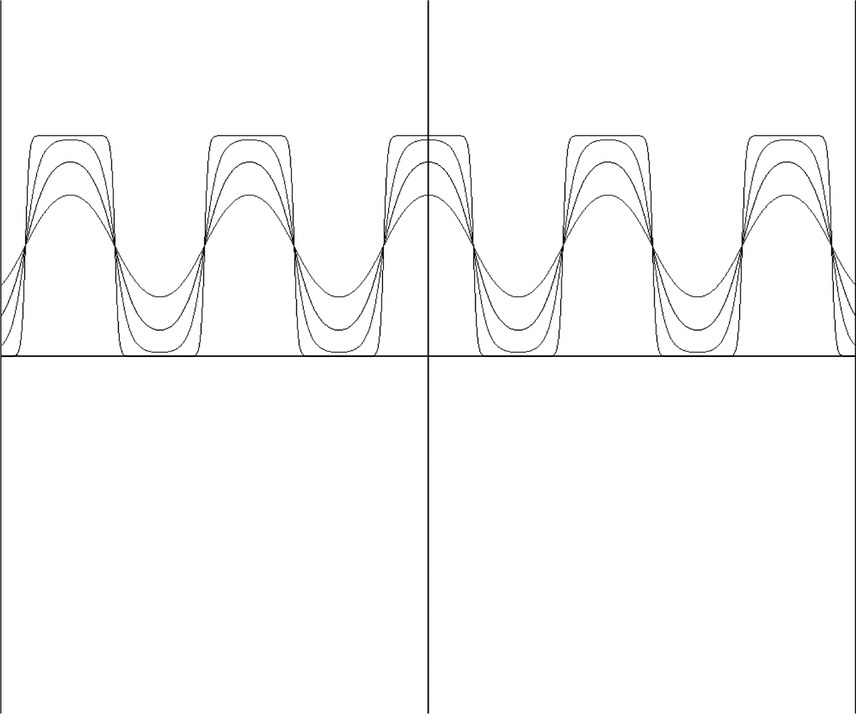
FIGURE 23-19 Collector output of an LM1458 differential pair for various input sine-wave input levels at 0.052, 0.104, 0.208, and 0.832 volt peak.
To observe the effects of slew-rate limiting, connect a sine-wave generator of amplitude = volts peak to peak to the input of the circuit in Figure 23-15. Start at 1 kHz and increase the frequency until the output signal at Vout1 changes from a sine wave to a triangle waveform. As the frequency increases, the sinusoidal signal at the (–) input of U1A in Figure 23-12 will increase sufficiently to cause limiting in the input stage and thus provide a square-wave current signal into the second stage of the LM1458 op amp. This square-wave signal then is fed to the second stage of the op amp that acts as a low-pass filter or integrator (Miller capacitance multiplier), which then results in the output waveform looking like a triangle wave.
We will now turn to a shunt feedback circuit for dividing resistance. The circuit in Figure 23-20 will demonstrate how shunt negative feedback provides an equivalent resistance that is lower than “expected.” High-impedance buffer amplifier U1B ensures current from the input voltage source only flows into R1. By setting the gain of U1A via the feedback resistor’s Rin = R1/(1 – – A) = R1/(1 1 A) = R1/(1 1 R3/R2). See Figure 23-20. In this case, R3 = R2; therefore,
![]()
With the voltage source a 1.5-volt battery and milliamp meter in series, as shown in Figure 23-20, measure the current flowing into R1. The current flowing into R1 should be about 3 mA. Therefore, by Ohm’s law, the equivalent resistance Rin, the resistance from R1 at the input to ground, should be 1.5 volts/3 mA = 500 ![]() .
.
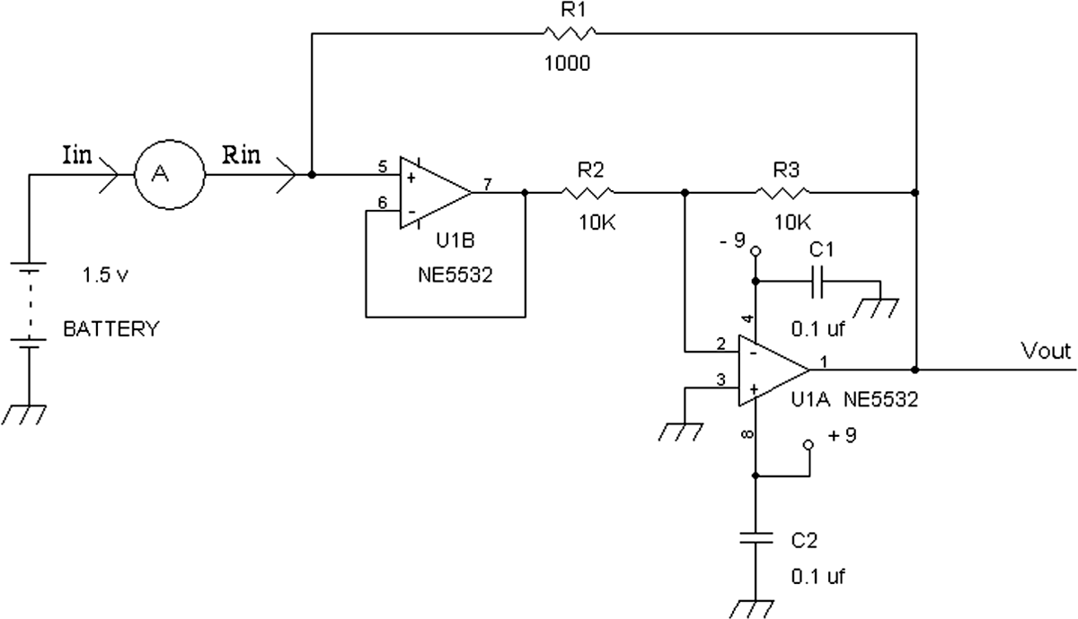
FIGURE 23-20 Resistance-value division circuit using a feedback resistor.
Alternatively, if the milliamp meter and 1.5-volt battery are removed, then Rin can be measured directly with an ohmmeter [e.g., a digital VOM (volt-ohm-milliammeter) or an analog VOM] at the R1–pin = U1B junction and ground.
If the gain of the inverting amplifier is increased, such as by replacing R3 with a 20-k![]() resistor instead, then A = 2, and the current drain will increase and provide an equivalent Rin = R1/(1 1 A) = 1,000/3 = 333
resistor instead, then A = 2, and the current drain will increase and provide an equivalent Rin = R1/(1 1 A) = 1,000/3 = 333 ![]() .
.
Similarly, this circuit works with AC signals as well (see Figure 23-21). Set an oscillator at 1 kHz and 1 volt peak to peak sine wave to Vin. Then measure the AC signal at R4/R1 or at the (1) input of U1B, which should read 0.5 volt peak to peak. By using “shunt” feedback to synthesize a resistor to ground via feedback resistor R1, a lower than expected resistance value is achieved because the output of U1A is providing a negative or out-of-phase signal to pull more current through R1.

FIGURE 23-21 AC signal into a divided resistance value.
Figure 23-22 shows another application of shunt feedback using a capacitor instead of a resistor. The result is again more than “expected” current flowing into the feedback capacitor, which mimics a larger capacitor from the input of U1B to ground. As a result of this larger than expected capacitor current via an out-of-phase signal at the output of U1A, the effective capacitance is increased. Therefore, Cin = (1 1A)C1.
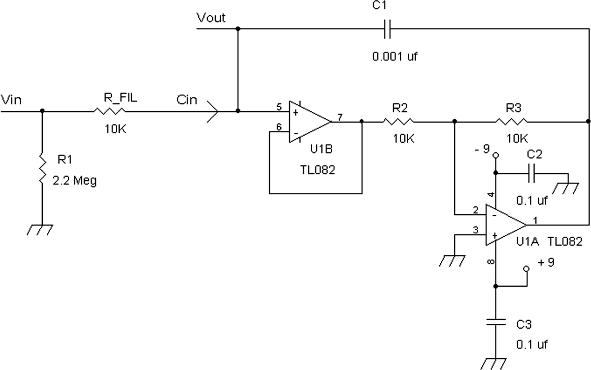
FIGURE 23-22 A capacitance multiplier circuit.
![]()
To ensure a DC bias potential at the (+) input of U1A with an AC coupled signal source, a large-valued resistor R1 = 2.2 MV is connected to R_FIL and ground. See Figure 23-22. With the shunt feedback capacitor C1 = 0.001 μF, and R_Fil = 10 k![]() , feed a sinusoidal signal of 1 V peak to peak at 100 Hz, and connect the scope probe to R_FIL/C1. With R3 = R2, the closed-loop gain A = 1; thus Cin = (1 + 1)C1 = 2(0.001 μF) = 0.002 μF = Cin.
, feed a sinusoidal signal of 1 V peak to peak at 100 Hz, and connect the scope probe to R_FIL/C1. With R3 = R2, the closed-loop gain A = 1; thus Cin = (1 + 1)C1 = 2(0.001 μF) = 0.002 μF = Cin.
The –3-dB (0.707 volt peak to peak) frequency then should be
![]()
With the oscillator’s frequency initially at 500 Hz, increase the oscillator’s frequency and confirm that the 1 volt peak to peak signal dropped to 0.707 volt peak to peak at around 8 kHz. One can experiment by replacing R3 with a 30-k![]() resistor to multiply the C1 capacitance by 1 1 3 = 4, which then results in Cin = 0.004 μF, or a –3-dB frequency at about 4 kHz.
resistor to multiply the C1 capacitance by 1 1 3 = 4, which then results in Cin = 0.004 μF, or a –3-dB frequency at about 4 kHz.
In operational amplifiers, usually the second stage includes a capacitance multiplier circuit (Miller multiplier) that multiplies the feedback capacitance value greatly with A >> 10 to ensure a unity-gain stable op amp. More information on Miller multipliers and compensating op amps can be found in the book, Analysis and Design of Analog Integrated Circuits, by Paul R. Gray and Robert G. Meyer (third edition, New York: John Wiley & Sons, 1993).
It should be noted that if R2 or R3 is replaced with a variable resistor, then Cin can be varied in capacitance values. Furthermore, if a voltage-controlled amplifier replaces R2, R3, and U1A, the capacitance value of Cin can be varied as a function of voltage. An example of a voltage-controlled variable capacitor using a variable-gain amplifier can be found in U.S. Patent 4,516,041.
And now for something completely different, well, sort of. Figures 23-23, 23-24, and 23-25 take me back to my college days when I had no proto boards to conveniently build or test circuits. But I did the next best thing. I used the old IBM 80 column computer programming cards as substrates or bases for holding down the electronic components. Since these IBM cards are not easily obtainable anymore, the circuits will be “taped” down on index cards instead.

FIGURE 23-23 Simple NPN current-source circuit.
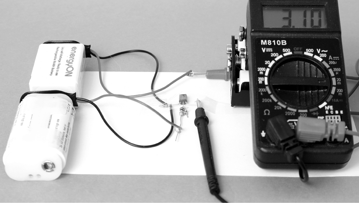
FIGURE 23-24 NPN current-source circuit assembled on an index card.
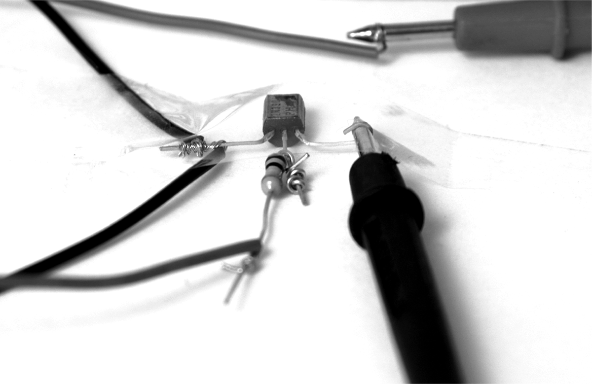
FIGURE 23-25 Close-up picture of index-card circuit board.
A simple current source is shown in Figure 23-23. The object of this experiment is to show that the current source changes very little in current even when the supply voltage is varied threefold. When the voltage is changed threefold across a resistor, the current changes by threefold, but this threefold increase is not so with a constant current source.
As mentioned earlier in this book, most people can relate to a constant voltage source such as a battery or power supply, which delivers a constant voltage “regardless” of the load current, within reason, of course. A constant current source delivers a constant current “regardless” of the voltage across it. In Figure 23-23, measure the collector current via a digital VOM at a supply voltage BT1 of 3 volts DC; then remeasure the collector current at 9 volts DC for BT1. Note that the current readings are almost the same at 3 volts and 9 volts for BT1, with very little increase in current when the supply voltage is raised. Also, the output resistance of this circuit can be determined by noting the change in voltage divided by the change in collector current. Rout is the resistance from collector to the (grounded) emitter. Thus
![]()
where ρVCE = 9 volts – 3 volts = 6 volts, and ΔIC = IC at 9 volts – IC at 3 volts.
Depending on the transistor, even with the same part number (e.g., 2N3904), the collector current can vary better than 2:1 owing to the current gain β of Q1. The collector current also affects the output resistance Rout because higher collector currents usually result in lower output resistance.
For this experiment, the following measurements were recorded:
IC at 9 volts = 3.10 mA
IC at 3 volts = 2.92 mA
Thus
![]()
However, because of the variation in current gain and other parameters among transistors, the reader should expect to see different results.
Figure 23-26 demonstrates another concept of a current source and its relationship with a load resistor. Thus Figure 23-26 shows a PNP constant current source with a resistive load. In this experiment, the DC current is essentially constant such that the voltage across the load resistor is determined by IC 3 RL = VCollector. First insert RL = 1 k![]() , and measure the voltage across the 1-k
, and measure the voltage across the 1-k![]() resistor. Then replace RL with a 3-k
resistor. Then replace RL with a 3-k![]() resistor and note that the voltage across the 3-k
resistor and note that the voltage across the 3-k![]() resistor has now increased threefold.
resistor has now increased threefold.
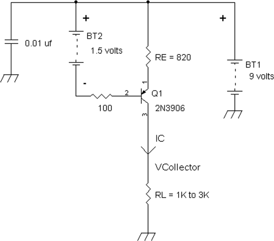
FIGURE 23-26 PNP constant-current-source experiment.
Experiments with a Resonant Circuit
Figure 23-27 shows a series resonant circuit that is used as a notch or band-reject filter. The AC voltages across the capacitor and inductor are out of phase by 180 degrees but are of the same magnitude at the resonant frequency
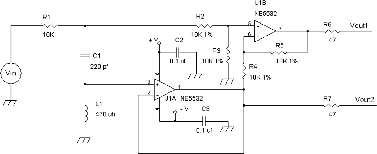
FIGURE 23-27 Experiment with a series resonant circuit.
![]()
With LI = 470 μH and Cl = 220 pF,
fres ≈ 495 kHz
Thus the series capacitor C1 and inductor L1 voltages add to zero (volt) at resonance (see Figure 23-27). This experiment will show that the voltage across capacitor C1 is indeed 180 degrees out of phase with the voltage across inductor L1. A voltage follower amplifier provides a voltage identical to the voltage across L1. A differential amplifier consisting of R2, R3, R4, R5, and U1B provides a signal indicative of the voltage across capacitor C1 at the output of U1B. With the values chosen for C1 and L1, the resonant frequency is about 500 kHz. Set the signal generator for 100 mV peak to peak at 500 kHz. Place a scope probe on C1/R1, and vary the frequency of the generator for minimum signal amplitude at C1/R1 to determine the resonant frequency, which should be near 500 kHz.
With a dual-trace display, Vout1 is on channel 1 and Vout2 is on channel 2 of the oscilloscope. Triggering of the signal can be chosen at channel 1 of the scope. Notice that the signals at channels 1 and 2 are about the same magnitude but opposite in phase. Therefore, there are AC voltages across the capacitor and inductor, but when these voltages are added in series, the resulting voltages cancel out (see Figure 23-28).
As seen in Figure 23-28, the top trace represents the voltage across capacitor C1, and the bottom trace represents the voltage across the inductor L1. Notice that the amplitudes are essentially the same but 180 degrees apart. The middle trace shows that summing the signals from the top and bottom traces results in zero or nearly zero.
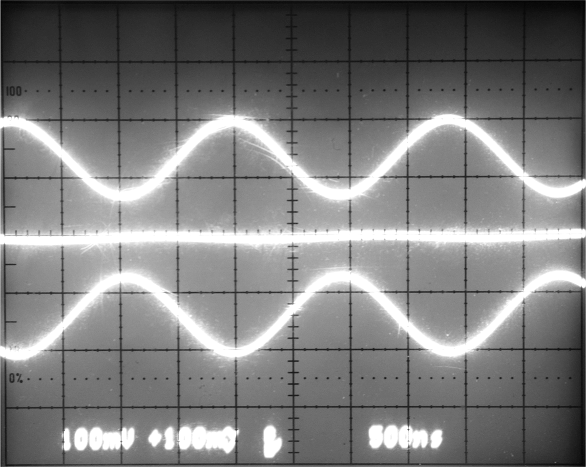
FIGURE 23-28 Dual-trace scope waveforms of voltages across C1 and L1 shown with the top and bottom traces.
For another experiment, one can sweep the signal with frequencies from 1 kHz to 1 MHz and observe the outputs at Vout1, which will provide a low-pass filter characteristic, and at Vout2, which has a high-pass-filter frequency response. With R1 = 10 k![]() , the Q of the circuit is generally too low for a low-pass or high-pass filter.
, the Q of the circuit is generally too low for a low-pass or high-pass filter.
![]()
where f res = ![]()
![]()
With R1 = 10 k![]() ,
,
![]()
which is a very low Q because the Q for a two-pole low-pass filter typically is
• ~0.577 for a Bessel filter, a more constant group delay filter for a linear phase response
• ~0.707 for a Butterworth filter, a maximally flat frequency-response filter
• ~1.0 for a slightly peaked filter
For example, change R1, which includes the output resistance of the generator, from 10 k![]() to 2,000
to 2,000 ![]() for a Butterworth filter. If the generator has a 600-
for a Butterworth filter. If the generator has a 600-![]() output resistance, then R1 should be about 1,400
output resistance, then R1 should be about 1,400 ![]() to provide a total resistance of 2,000
to provide a total resistance of 2,000 ![]() .
.
One may ask why such a low Q for low-pass or high-pass two-pole filters? The reason is that generally low-pass and high-pass filters provide a wide bandwidth frequency response as opposed to band-pass filters, which have a much narrower bandwidth. Typical band-pass two-pole filters require a Q > 2 (e.g., for video chroma subcarrier band-pass filters centered at 3.58 MHz or 4.43 MHz, the Q is typically between 2 and 5.) and Q > 10 for RF/IF filter circuits. Recall that high-Q circuits provide narrow bandwidth, and low-Q circuits result in wide bandwidth.
Thevenin-Equivalent Circuit
One of the most common circuits is a voltage-divider circuit using two resistors R1 and R2 that attenuates or divides the amplitude of a signal. A Thevenin-equivalent circuit of a voltage-divider circuit uses the values of the two resistors and the original voltage source to “transform” the voltage-divider circuit to a lower-voltage source and a single resistor (Figures 23-29 and 23-30).
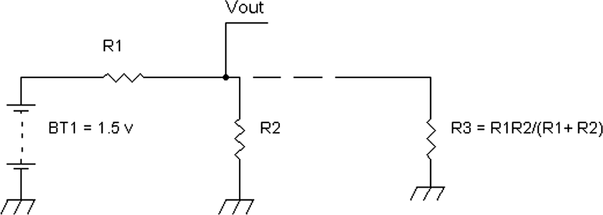
FIGURE 23-29 A simple two-resistor voltage-divider circuit.

FIGURE 23-30 A Thevenin-equivalent circuit to the voltage-divider circuit.
One characteristic of reducing a voltage-divider circuit to a Thevenin-equivalent circuit is that the source resistance or Thevenin resistance is now known as the parallel combination of R1 and R2. Therefore, one can almost use the resistive divider circuit like a step-down transformer. But unlike a transformer that preserves power transfer, a resistive divider circuit creates losses in power.
The divided down-voltage via voltage source BT1, loading into an open circuit then is
![]()
In general BT1 = an arbitrary voltage Vin, and so
For example, dividing down the voltage allows for providing a low-impedance source. Therefore, to confirm that the Thevenin-equivalent circuit really works in that
![]()
let R1 = R2 = 20 k![]() so that
so that
![]()
A cell or battery, such as a 1.5-volt battery = Vin, provides the voltage to R1 = 20 k![]() as shown in Figures 23-29 and 23-30. The voltage at R2 = 20 k
as shown in Figures 23-29 and 23-30. The voltage at R2 = 20 k![]() then should measure as
then should measure as
![]()
Now take a 10-k![]() resistor for R3 and connect it in parallel with R2. If the Thevenin resistance is indeed 10 k
resistor for R3 and connect it in parallel with R2. If the Thevenin resistance is indeed 10 k![]() , which is now the source resistance, paralleling R3 = 10 k
, which is now the source resistance, paralleling R3 = 10 k![]() should drop the 0.75 volt to half, or 0.375 volt.
should drop the 0.75 volt to half, or 0.375 volt.
One can try different voltages and values for R1 and R2 to confirm the Thevenin voltage and resistance. For example, use a 9-volt battery for Vin, and let R1 = 47 k![]() and R2 = 2.7 k
and R2 = 2.7 k![]() . Then
. Then
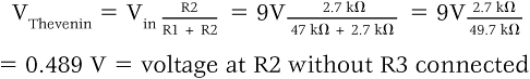
![]()
If 2.55 k![]() = R3, now connect R3 across R2, and the 0.489 volt should drop by half to 0.2445 volt.
= R3, now connect R3 across R2, and the 0.489 volt should drop by half to 0.2445 volt.
The Thevenin-equivalent circuit also is applicable to AC voltage sources. With AC signals, one can use either a resistive or a capacitive voltage divider. Therefore, the voltage-divider circuit sometimes can be used as a minimum-loss pad circuit for impedance matching (e.g., from high to low impedance).
Analyzing a Bridge Circuit
Figure 23-31 shows a bridge circuit with current flowing through R3 as the particular DC current of interest. R3 may represent an ammeter such as a galvanometer’s coil resistance, and R1 and R2 are the same resistance. In a Wheatstone bridge circuit, normally an unknown resistor such as R5 is inserted and a known calibrated variable resistance in R4 is varied until there is no current flowing into R3. When the null in current through R3 is achieved, the calibrated resistance value is read off R4.
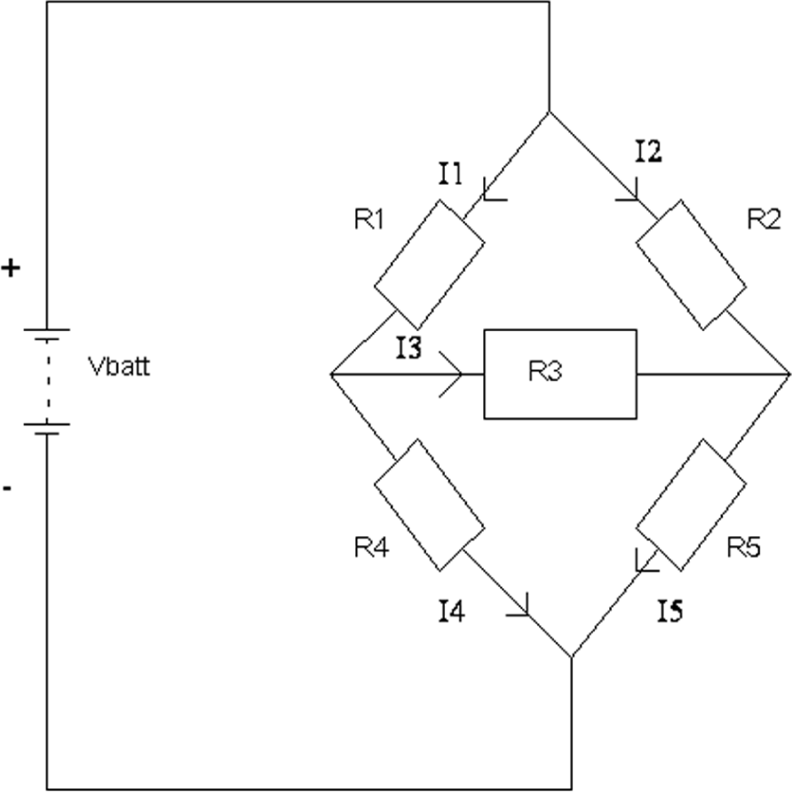
FIGURE 23-31 A bridge circuit.
For this experiment, suppose that we want to find the current through R3 for any value of R1, R2, R3, R4, and R5 for a given voltage supply. How would one start to solve the equations? Five currents are identified as I1, I2, I3, I4, and I5, and the five resistors, R1, R2, R3, R4, and R5, are shown, along with a known voltage Vbatt. We have five unknown currents and need to set up five equations to solve for the current through R3. Or do we?
Is there a faster way to solve for I3, and if so, how is it done? These and other questions enquiring minds would like know. Therefore, the strategy to solve this problem is to “Get Smart.”
Would you believe that this problem can be solved in 99 seconds? Or how about 86 seconds? (See the TV show Get Smart.) Actually, this problem can be solved in 20 seconds or less. Of course, one may say, “Surely you are joking!” and my response would be, “I am not joking... and don’t call me Shirley!” (See the movie Airplane!).
Okay, kidding aside, the bridge circuit can be split and analyzed by converting the four outer resistors into two Thevenin-equivalent circuits (see Figures 23-32 and 23-33).
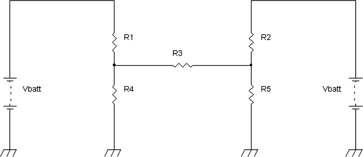
FIGURE 23-32 The bridge circuit is redrawn with a ground reference and two voltage-divider circuits.

FIGURE 23-33 The circuit in Figure 23-32 is redrawn as two Thevenin-equivalent circuits.
The voltage divider consisting of R1 and R4 with Vbatt is equivalent to a Thevenin-equivalent circuit with
![]()
and the Thevenin resistor is just the parallel combination of R1 and R4; that is,
![]()
Similarly for the voltage divider consisting of R2 and R5, the Thevenin voltage and resistor are
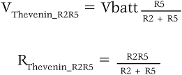
With R3 bridging or connecting the two Thevenin circuits, the current through R3 is reduced to one equation and one unknown. Thus

One can further simplify I3 as
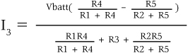
So there you have it, the answer for I3, which is the current through resistor R3 solved within 20 seconds if your handwriting is quick enough. And if you solved the problem in 21 seconds instead, a famous TV (or movie) secret agent would say to you, “Missed it by that much!” Actually I am kidding now, and solving the problem in 21 seconds to a few minutes is fine.
Of course, one actually can see if this analysis works. Set Vbatt = 9 volts; R1 = R2 = R3 = R4 = 20 k![]() ; and R5 = 10 k
; and R5 = 10 k![]() . The current through R3 should be
. The current through R3 should be

With 5 percent resistors for R1 = R2 = R3 = R4 = 20 k![]() , R5 = 10 k
, R5 = 10 k![]() 1 percent, and Vbatt = 9 volts, the measured I3 = 39.5 μA, which is very close to the calculated value of 40.9 μA.
1 percent, and Vbatt = 9 volts, the measured I3 = 39.5 μA, which is very close to the calculated value of 40.9 μA.
Some Final Thoughts on the Book
When I worked at Ampex, the company that invented the first practical videotape recorder, my mentor told me that in school you learn how to learn, and after you have completed your studies, then comes the real learning. Learning electronics or almost anything, for that matter, is a lifelong process. What I have found is that we all become to some degree self-taught in our subsequent studies. For instance, I learned the subject of noise from reading books and asking questions of experts in the field. I also had two or three great mentors who showed me the ropes in designing circuits. So, if you can find a mentor, please learn as much as you can from him or her. Experience counts a lot!
So, for me, I am always exploring electronics and related subjects such as math. And although readers may think after reading Chapters 13 through 22 that I am too math-centric, these particular chapters were written to show how the math is used to explain signals and circuits but not how to necessarily design circuits. However, I also will take knowledge from history and music as well for finding a solution to an engineering problem. One key to invention is the integration or merging and picking and choosing from the various knowledge bases. For example, one of my audio scrambling patents utilized timing signals in a form of “Rubato,” or stolen time. Rubato is a way of playing music where the tempo speeds up and slows down for emotional effect.
There are many approaches to designing analog circuits. And the readers should know that I am a circuit designer first, as can be seen in Chapters 4 through 12. That is my usual “state.” One approach is to scope out the analog design or problem mathematically and then design, which can be verified by a simulation program such as PSPICE and/or by building the circuits and testing them. The other approach is to design by intuition based on lots of experience and judgment and then later to analyze mathematically/scientifically why the design worked. I tend to switch back and forth between these two methods, but at the end of the day, I want to ensure that the design works both by practice and by theory. Just having an analog design work without full scrutiny sometimes is not good enough in terms of reliability or repeatability of the circuit.
This book is really meant for self-teaching by anyone who is interested in electronics. The math, although voluminous, really never gets too complicated beyond algebra and trigonometry. When I explain technology to people, I generally do not use too much math at all, but if I know that the person has some math, even algebra, I can include “simple” mathematics in my tutorials.
What the reader also should take away from this book is that designs do not always work the first time, even when “every” detail had been taken into account. But perseverance is one of the keys to successful problem solving. For example, one of my first full-blown video designs involved designing a miniature TV monitor, a cathode-ray tube (CRT) viewfinder for a TV camera. The problem I was having was that the horizontal scanning system was nonlinear, causing people to literally change width or weight as they moved across the displayed TV frame. I tried various conventional approaches that got close but not good enough. And because of a space constraint, I could not use a linearity coil. So I was stuck for two weeks not producing a solution. Finally, I solved the problem by applying negative feedback in an unconventional manner and sending a correction waveform via the damper diode.
There are times when a solution to a particular problem is not accessible through the Internet, books, or papers. Thus the particular problem has to be reduced to: What is the real problem? Finding out the main problem takes time. For example, in Chapter 7, the project was to show a transistorized regenerative radio. I thought it would be easy because my tube version performed straight from the get-go. What I found, however, was that the first try ended up with very poor sensitivity. I had to literally get out and take a hike for about half an hour before I realized why the radio was going into oscillation too soon, and by the time I finished the hike, I figured out a solution. During the hike, I figured out that there was insufficient radio-frequency (RF) gain for demodulation without applying regeneration, and I was trying to apply regeneration to bring up or compensate for a weak RF signal. However, because the RF signal was much too low in strength, the radio broke into oscillation instead when the regeneration control was turned up. Therefore, the solution was to first provide enough RF signal and then devise a way to control the regeneration (positive-feedback signal) in a manner that allowed the demodulation of the amplitude-modulated (AM) signal.
Therefore, designs do not always work as planned. But keep at it, and if you are stuck, take a shower, go to the park, get out of the office, and/or get some sleep.
Writing this book has been a fantastic journey for me, as well as a great learning experience. Well, that is all I have to say—except thank you for your interest. And after writing over a 100,000 words, I think I will watch some cartoons and listen to “The Merry Go-Round Broke Down.” So... That’s all folks!
References
1. Class Notes EE141, Paul R. Gray and Robert G. Meyer, UC Berkeley, Spring 1975.
2. Class Notes EE241, Paul R. Gray and Robert G. Meyer, UC Berkeley, Fall 1975.
3. Class Notes EE140, Robert G. Meyer, UC Berkeley, Fall 1975.
4. Class Notes EE240, Robert G. Meyer, UC Berkeley, Spring 1976.
5. Paul R. Gray and Robert G. Meyer, Analysis and Design of Analog Integrated Circuits, 3rd ed. New York: John Wiley & Sons, 1993.
6. Kenneth K. Clarke and Donald T. Hess, Communication Circuits: Analysis and Design. Reading: Addison-Wesley, 1971.
7. Mischa Schwartz, Information, Transmission, and Noise. New York: McGraw-Hill, 1959.
8. William G. Oldham and Steven E. Schwarz, An Introduction to Electronics. New York: Holt, Reinhart and Winston, Inc., 1972.
9. Allan R. Hambley, Electrical Engineering Principles and Applications, 2nd ed. Upper Saddle River: Prentice Hall, 2002.
10. Murray H. Protter and Charles B. Morrey, Jr., Modern Mathematical Analysis. Reading: Addison-Wesley, 1964.
11. Texas Instruments, Linear Circuits Amplifiers, Comparators, and Special Functions, Data Book 1. Dallas: Texas Instruments, 1989.
12. Motorola Semiconductor Products, Inc., Linear Integrated Circuits, Vol. 6, Series B., 1976.
13. Thomas M. Frederiksen, Intuitive IC Op Amps from Basics to Useful Applications (National’s Semiconductor Technology Series). Santa Clara: National Semiconductor Corporation, 1984.
14. Alan B. Grebene, Bipolar and MOS Analog Circuit Design. New York: John Wiley & Sons, 1984.
15. U.S. Patent 4,516,041, Ronald Quan, “Voltage Controlled Variable Capacitor,” filed on November 22, 1982.
16. U.S. Patent 5,058,159, Ronald Quan, “Method and Apparatus for Scrambling and Descrambling Audio Information Signals,” filed on June 15, 1989.