Chapter 14
Mixer Circuits and Harmonic Mixers
An idealized mixer is a multiplier circuit that takes two signals and literally multiplies the values of each signal to provide an output. In one sense, this concept is easier to understand with multiplication of numbers. For example, there are two analog signals, each connected to an analog-to-digital converter (ADC). The digital outputs from the two ADCs then provide numbers from each signal, and these numbers are updated over time. If the outputs of the ADCs are fed to a digital multiplier, then the output of the digital multiplier will provide a stream of numbers that are the product of the two streams of numbers from the outputs of the ADCs. The output of the digital multiplier then is connected to a digital-to-analog converter (DAC) to provide an analog signal that represents the product of the two analog signals.
But back in the days of the superheterodyne radio in the late teens of the twentieth century, multiplication, or an approximation of it, had to be done all in the analog domain. Therefore, vacuum tubes such as triodes and pentodes were used commonly to provide an analog multiplication effect of two signals such as the radio-frequency (RF) signal and the local oscillator signal. For the triode, which is a very linear amplification device, a very large local oscillator voltage was supplied to its cathode or grid to essentially turn the triode on and off to cause a chopping effect on the RF signal such that the output signal at the plate of the triode provided an intermediate-frequency (IF) signal.
Pentodes were handled similarly to triodes in terms of RF mixing, with the oscillator signal and RF signal combined in the control grid. The pentode had a screen grid, and transconductance depended on the voltage supplied to the screen grid. Usually, the screen grid was connected to a direct-current (DC) source to set a fixed transconductance. However, some mixer designs connected the RF signal to the control grid, whereas the local oscillator’s signal was connected to the screen grid to modulate the transconductance of the pentode. The modulated transconductance then provided a multiplying effect of the RF signal.
But other analog multiplying methods and circuits also were used in the early years of radio. For example, diodes could be used as mixers or as part of a more complex mixer circuit such as a double-balanced modulator. And in particular, in the late 1920s or by 1930, switch-mode mixers using solid-state copper oxide diodes were used in commutating switch-mode mixers or balanced modulators.
Mixers can be viewed in two ways:
1. Two (or more) signals are applied to a nonlinear device to generate distortion and thus provide an IF signal.
2. Or more commonly, mixers are symbolized as multipliers that generate an output signal that is the product of two (or more) input signals.
Thus the objective for this chapter is to cover analog mixer circuits. Switch-mode mixers will be explained in Chapter 15.
Adding Circuits Versus Mixing Circuits
Analog circuits that are adders will sum or combine two signals without distortion signals at the output. The output is just the summation of the two input signals. Figure 14-1 shows various examples of summing circuits. The top circuit is a simple two-resistor signal-combining network. And the bottom circuit shows an operational amplifier (op amp) summing circuit that has an output of

FIGURE 14-1 Examples of summing circuits.
![]()
Mixing circuits, however, are nonlinear in nature. When two signals are combined into a mixer circuit, either by modulation and/or by nonlinearities of the mixer circuit, signals at the output of the mixer contain distortion products related to harmonics and intermodulation of the two signals (Figure 14-2).
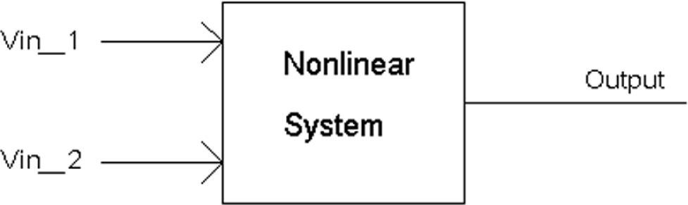
FIGURE 14-2 A mixer system with nonlinearities that generate distortions.
First, let’s look at harmonic distortion. Harmonic distortion simply means that the output of the mixer generates a signal that is at least one multiple (2, 3, 4,... ) of the input frequency. So, for example, a junction field-effect transistor (FET) has approximately a square-law relationship of the following:
![]()
where Vgs is the gate-to-source voltage, Vp is the cutoff voltage of the FET, and is a constant based on DC current when the gate-to-source voltage Vgs = 0. From expanding the equation, we get
![]()
Note that the first term in the brackets is 1, a DC current term, whereas the second term in the brackets is a linear-amplification term, –2(Vgs/Vp) where Vgs contributes to the output current Iout. However, the third term, +(Vgs/Vp)2, squares the input signal across the gate and source of the FET.
Now let’s take a look graphically at what squaring a signal means (Figure 14-3). The input signal is an alternating-current (AC) signal that has a range of positive and negative voltages, but the squared input signal is nonnegative, which includes 0 and positive voltages only and at twice the frequency of the input. As one can see, the squaring of the input signal results in a second harmonic signal.

FIGURE 14-3 Squaring a sinusoidal signal produces a twice-frequency component. The X axis shows time, whereas the Y axis shows the amplitude.
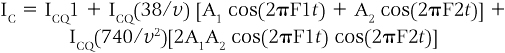
So what happens if the input signal is a combination of two signals of different frequencies? Figure 14-4 shows two “high” frequency signals with frequencies F1 and F2 in the lower portion that are just slightly different in frequency. The smaller-amplitude high-frequency signal (with a frequency of F1) is lower in frequency than the higher-amplitude high-frequency signal (with a frequency of F2). When these two signals are added (summed) and squared, the resulting waveform is seen at the top of the figure and resembles an amplitude-modulated (AM) waveform. The envelope of the signal at the top of the figure has a frequency that is the difference of the two high-frequency signals with a frequency of F2 – F1.
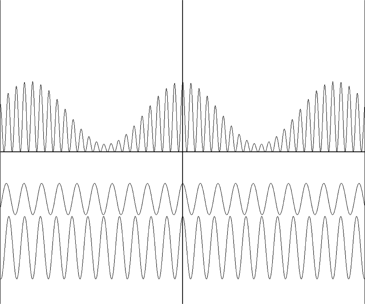
Figure 14-4 Two “high” frequency signals that are combined and squared, resulting in a modulating waveform. The X axis shows time, whereas the Y axis shows the amplitude.
So, clearly, a nonlinear device causes a modulation effect, which, in turn, causes a mixing effect. If we just substitute two sinusoidal signals of frequencies F1 and F2 into a squaring function, we get the following:
![]()
Note that the first and third terms, [cos(2μF1t)]2 and [cos(2μF2t)]2, will generate second harmonics of each of the two input signals, and more important, the middle term shows multiplication of the two input signals.
From a trigonometric identity, 2[cos(α)][cos(β)] = cos(α + β) + cos(α – β) and in particular, that middle term
![]()
Note that the squaring function provides both a difference-frequency term (F1 – F2) and a summing-frequency term (F1 + F2). And it should be noted that signals that carry the difference- and summing-frequency terms are intermodulation distortion products or signals.
And in superheterodyne receivers, the IF signal from the mixer has a difference frequency such as (F1 – F2), where F1 is the frequency of the local oscillator, and F2 is the frequency of the input RF signal.
Distortion Can Be a Good Thing (for Mixing)
We have seen how an FET with an approximate square-law characteristic can act as a linear summer and as a mixer/multiplier. This square-law characteristic generates distortion in terms of harmonic and intermodulation distortion products at the drain of the FET.
FETs are used as mixers, and often to provide good mixing action. Typically the local oscillator’s voltage (i.e., combined with the RF signal) is in the amplitude level of volts peak to peak. The reason for this is that the FET is such a linear device that huge amounts of input voltage are required to drive the FET into “usable” distortion that provides adequate levels of the IF signal.
Single-Bipolar-Transistor Distortion
Now suppose that we would like to use a bipolar transistor for mixing. As mentioned previously, a bipolar-transistor amplifier with its emitter grounded AC-wise has an exponential function:
![]()
where VBE is the total voltage across the base emitter junction of the transistor, which includes a DC bias voltage VBEQ plus the AC signal voltage Vsig. Thus
![]()
The collector current can be expressed equivalently as
![]()
The DC or quiescent collector current is just
![]()
Figure 14-5 presents an example of a common emitter amplifier. In the figure, a common emitter amplifier with β > 100, the DC emitter current is essentially equal to the DC collector current. Thus VE/RE = ICQ.
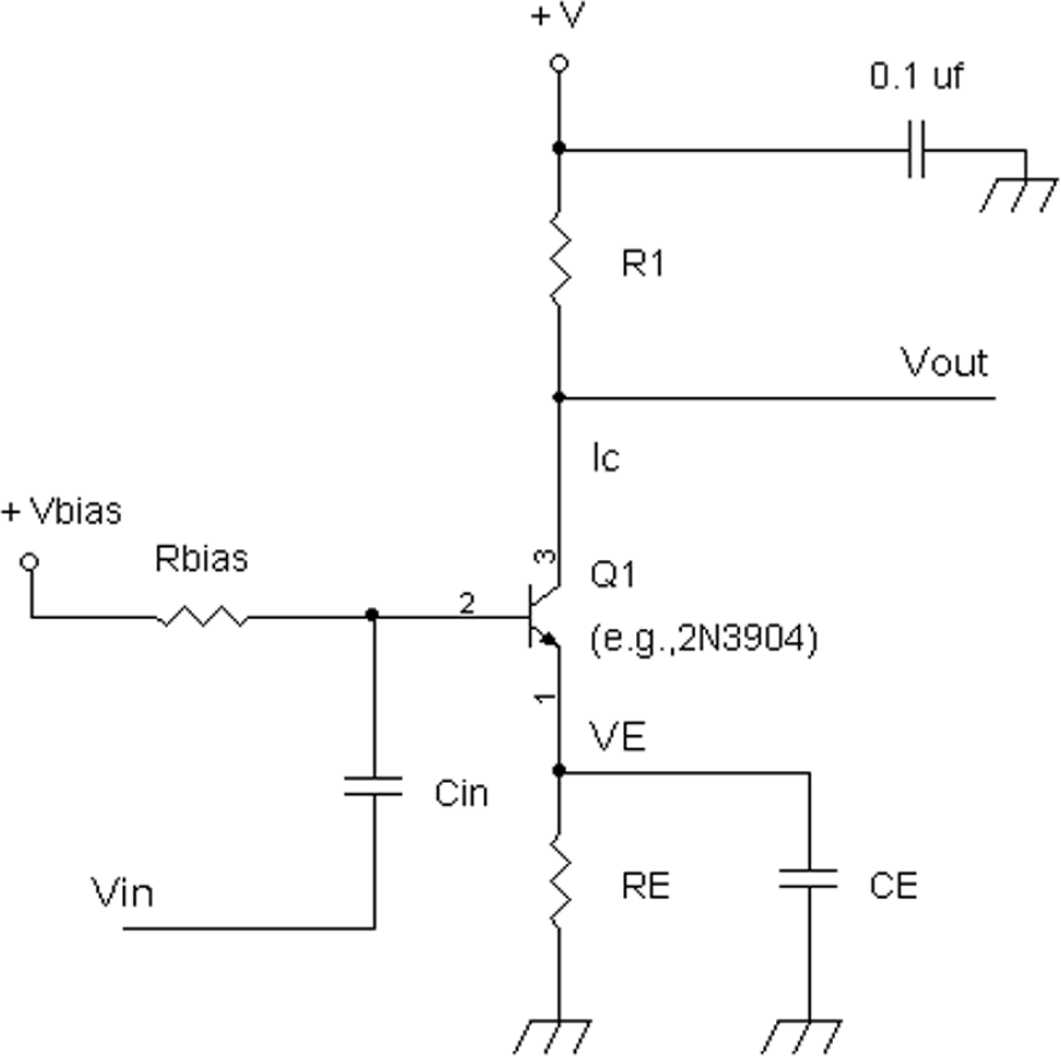
FIGURE 14-5 A common emitter amplifier.
Note that (eVsig/(KT/q)) is a modulating factor of the DC quiescent collector current and represents the AC signal or time-varying signal in the collector current.
So what about the “mysterious” term (eVsig/(KT/q))? What is that equal to? in Chapter 13 with the introduction to e, it was stated that e = 2.71828... = e1. And one way to calculate e is
![]()
And
![]()
where n! is not yelling out n with great loudness (a high school joke), but n! is n factorial:
![]()
For example,
![]()

The preceding general equation is rather daunting. But generally, we are concerned only with a few or at most the first four terms of this equation. If more terms are to be calculated, there are computers to do that!
Now let’s use the preceding general equation to figure out what happens when
![]()
and
![]()
with v in units of volts.
And we will just calculate the first three or four terms:
![]()
By using Equation (14-5),
![]()
this then leads to the collector current being equal to
![]()
The equation for the collector current shows that there is a squared term and a cubic term that will (at least) provide distortion of the second and third orders. From Equation (14-1) on the FET’s square-law characteristic, a modulation effect on two signals occurs with the squared term. Since the bipolar transistor also includes a squared term, we can expect that the bipolar transistor will generate a modulation effect with two input signals as well. And this modulation effect is what we are looking for in a single-bipolar-transistor mixer.
It should be noted that the generalized Equation (14-9) is really only valid for peak sinusoid waveforms of about 26 mV or less. At input signals of 26 mV peak, the equation holds up very well in determining harmonic distortion. Higher-amplitude sinusoidal waveforms of 50 mV or more peak will cause gain compression, and predicting the harmonic distortion will become inaccurate. Therefore, for the higher amplitude signals, modified Bessel functions are used instead of the power series expansion in equation (14-9).
Before moving on to how harmonic and intermodulation distortion is calculated, we should review Equation (14-9):
![]()
Spreading out the terms, we get
![]()
Now let’s look at the first four terms and see what they represent.
1. ICQ 1 = ICQ is DC collector current or bias current.
2. ICQ(38/v)Vsig = is the linear amplification term. The small-signal transconductance gm = ICQ (38). For example, at 1 mA of ICo, the DC collector current results in 38 mA/V for the small-signal transconductance. And 100 μA of ICQ results in 3.8 mA/V of small-signal transconductance.
3. ICQ(740/y2)Vs2sig is the square-law term that generates a DC offset plus second-order harmonic and intermodulation distortion. Second-order intermodulation distortion from two signals of frequencies F1 and F2 results in output signals with frequencies of (F1 1 F2) and (F1 – F2).
4. ICQ(9,467/v3)Vs3sig is the cubic term, which produces third-order harmonic and intermodulation distortion. For two signals at the input of F1 and F2, the third-order intermodulation signals are more complicated than the second-order intermodulation components. The third-order intermodulation distortion products for the two input signals will generate signals that have frequencies of (2F1 – F2), (2F2 – F1), (2F1 1 F2), and (2F2 1 F1).
To calculate distortion, such as second- or third-order distortion, Vsig is set to a single or multiple sinusoidal signals. For mixing purposes, there are generally two signals at the input of the mixer, the RF signal and the local oscillator signal. Thus, for now, we will not concern ourselves with harmonic distortion but just concentrate on second-order intermodulation distortion because it is this distortion product that generates the difference-frequency signal (F1 – F2).
Consider the input two sinusoidal waveforms from Equation (14-2):
![]()
Let’s generalize the amplitudes of each input signal with A1 and A2 such that
![]()
which then yields the square-law term:

Because we are interested only in the “modulated” or multiplying term between the two signals, the second term is of interest, which then reduces to
![]()
So now, if we return to Equation (14-10) for just the first three terms, we have
![]()
and if we substitute for the two signals at the input for Vsig and refer to equations (14-11) and (14-12), we have

Removing or ignoring the second-order harmonic distortion terms [A1 cos(2πF1t)]2 and [A2 cos(2πF2t)]2, we get
And using Equation (14-13) for substitution, we arrive at

So what does Equation (14-14) really mean? For determining the intermodulation distortion products and the difference-frequency term, this equation is really accurate for signals of less than about 13 mV peak. Any larger signals will start to include errors, and these errors will increase as the input signal’s amplitude rises above 26 mV peak.
Let’s try the following scenario: The signal A1 cos(2πF1t) is the oscillator signal with A1 = 0.013. A2 is the RF input signal with A2 < 0.013 volt (e.g., typically = mV or less). The second-order intermodulation distortion IM2 as a function of one of the input signals is
![]()
Note: (ICQ740/ICQ38) = (ICQ/ICQ) (740/38) = 1(740/38) = 19
But what does this 25 percent of IM2 distortion mean? This means that the IM2 distortion components have an equivalent transconductance of 25 percent of the small-signal transconductance. So, if the transistor is biased at 1 mA, the transconductance for generating the sum- or difference-frequency signal is 25%(gm = 25%(0.0384) A/V, or 9.5 mA/V.
So, for example, for an oscillator signal of 0.013 volt peak sinusoidal waveform added or combined with a small-signal RF signal VRF into the base and emitter junction of a bipolar transistor amplifier operating at 1 mA, the IF signal current Isig-IF with the difference frequency is
![]()
Note that the conversion transconductance is Isig_IF/VRF. And for a 0.013-volt peak sinusoidal oscillator signal into the mixer, the conversion transconductance is 25%(gm).
Equation (14-15) shows that the conversion gain or IF signal transconductance is controlled by the oscillator’s signal amplitude. But it should be noted that increasing the oscillator’s peak amplitude A1 beyond 0.013-volt will raise that 25 percent number to something higher that is no longer linear or proportional. By using other mathematical techniques that are more accurate than the power-series expansion [e.g., Equation (14-8) or (14-9)], it is found that if the oscillator signal is raised to 26 mV peak, or 2 3 13 mV peak, we get 45%(gm) instead of 50%(gm) for the conversion gain.
In previous chapters concerning the superheterodyne radio, it was mentioned that the oscillator voltage into the mixer or converter is in the range of about 200 mV to 300 mV peak to peak or 100 mV to 150 mV peak. The next section will explore a more accurate model for bipolar mixer circuits with large oscillator voltages that are beyond 13 mV peak.
Another technique to more accurately characterize the behavior of a simple transistor mixer is to view the transistor as having a time-varying transconductance that depends on the oscillator signal. Recall that the small-signal transconductance gm = ICQ/(0.026 volt). Usually we define a small-signal transconductance as gmQ = ICQ/(0.026 volt), where ICQ is a constant DC current, which then makes gmQ a constant small-signal transconductance.
But when an oscillator voltage is added with the bias voltage, the collector current is actually time-varying, and thus the transconductance is changing with time in relation to the amplitude and frequency of the oscillator signal. Therefore, the output collector current as a function of time can be thought of as
![]()
where gm(t) is a time-varying transconductance with its shape depending on the oscillator amplitude. This shape resembles the collector current of a bipolar transistor with a large overdrive signal, as seen in Figure 14-6. For large signals such as 100 mV to 200 mV peak to peak, the time-varying transconductance has a shape approaching a pulse. And the narrowing nature of this pulse as larger and larger amplitudes of oscillator signals are combined into a transistor mixer will limit the conversion transconductance.
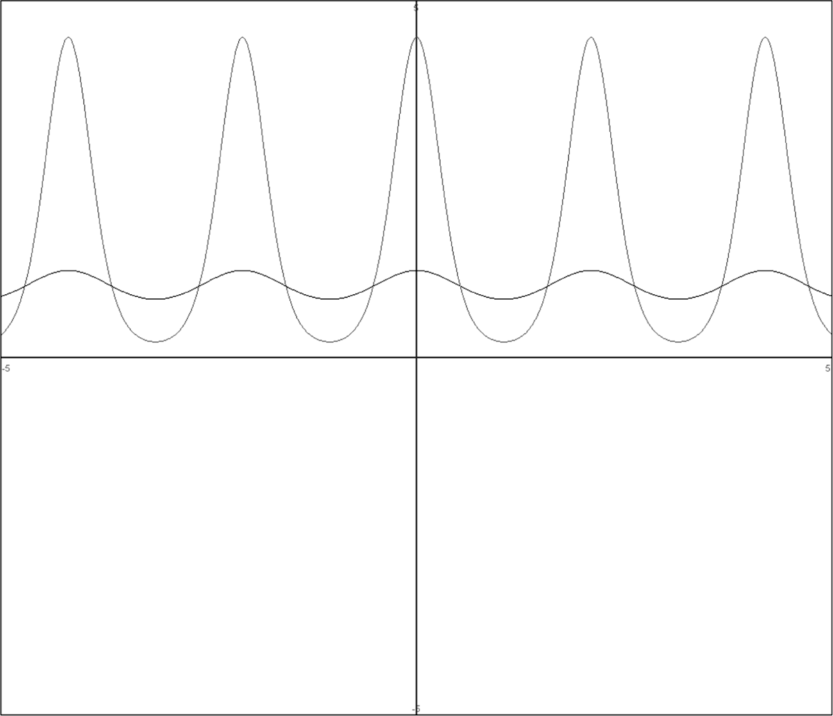
FIGURE 14-6 Collector current of the transistor for various input levels into the base-emitter junction. The X axis shows time, whereas the Y axis shows the amplitude.
As seen in the figure, because transconductance is directly related to the collector current, the transconductance is time-varying and has the same pulse “shape” as the oscillator amplitude is increased into the transistor mixer. A topic of mathematics known as modified Bessel functions explains the time-varying transconductance of a bipolar transistor mixer. Modified Bessel functions are rather involved, and they generally are taught in senior year or graduate school university classes. I will take a simplified approach instead, just showing the results of the conversion transconductance as a function of oscillator signal injection voltage.
Simple Transistor Mixer and Its Conversion Transconductance
Let me say at this point that I have probably overloaded quite a few readers with equations and trigonometric identities to explain how distortion in amplifiers is used in mixers or modulators. So this next section will detour back to a tabulated approach. After all, the math can be interesting but also can sidetrack the reader.
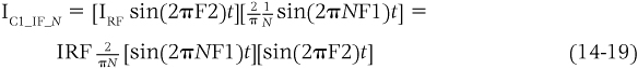
See Figure 14-7, a simple one-transistor mixer. Figure 14-7 is a simple transistor mixer circuit whereby the oscillator signal is combined with the RF signal to provide typically an IF signal. Table 14-1 lists the tabulated ratios of conversion transconductance to small-signal transconductance as a function of the oscillator signal’s peak amplitude.
FIGURE 14-7 A simple transistor mixer circuit.
TABLE 14-1 Ratio of Conversion Transconductance to Small-Signal Transconductance for the Sum- or Difference-Frequency (F1 ± F2) Signals as a Function of the Oscillator Signal’s Peak Amplitude
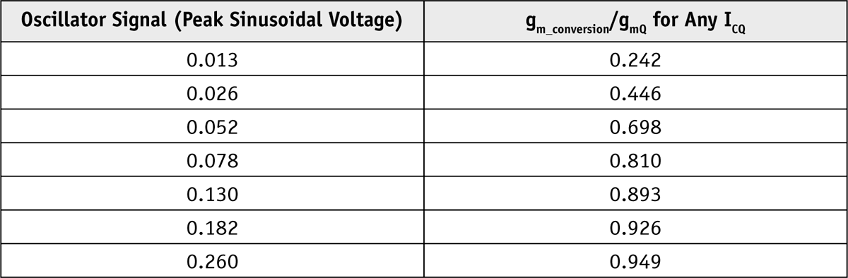
As can be seen in Table 14-1, there is a law of diminishing returns, and generally, an oscillator signal of at least 100 mV peak to peak will provide sufficient drive. Table 14-2 shows the conversion transconductance at 1 mA DC collector current.
TABLE 14-2 Conversion Transconductance at 1 mA as a Function of Oscillator Drive Voltage
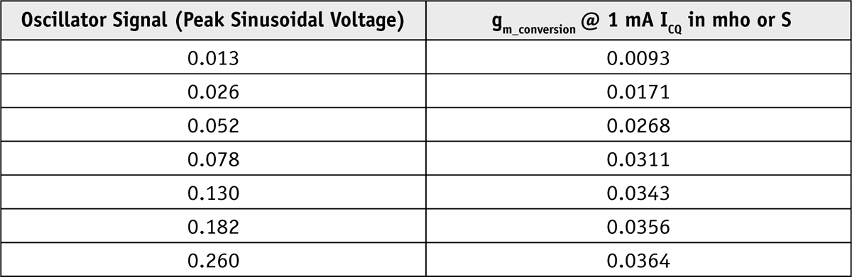
Since the conversion transconductance gm_conversion is proportional to the DC collector current, the numbers in the right column of Table 14-2 can be scaled appropriately. For example, to find gm_conversion at 2 mA, just multiply the numbers by 2, and to find gm_conversion at 100 μA, just divide the numbers by 10. Again, the values for gm_conversion are only for output signals that provide frequencies of F1 – F2 or F1 + F2.
For a quick example, suppose that the oscillator injects a 78-mV peak sine wave into the mixer. What would be the conversion gain for an IF tank circuit with an equivalent parallel resistance R = 150 k![]() when the DC collector current is 100 μA?
when the DC collector current is 100 μA?
The conversion gain is gm_conversion × R. At 1 mA for 78 mV peak,
so 100 μA is one-tenth of 1 mA, which leads to
![]()
Therefore, the conversion gain is 0.00311 mho × 150,000 V = 466. This would mean that an RF signal is amplified 466 times and converted to an IF signal of generally lower frequency. For example, if the RF signal is 1 mV peak to peak at 600 kHz and the local oscillator provides a 1,055-kHz signal at 78 mV peak with a 100-μA DC collector current for the one-transistor mixer and a 150-V load at 455 kHz, the output IF signal at 455 kHz will be 466 mV peak to peak.
Also, it should be noted that because the RF signal is generally small, the worst case or minimum input resistance into the base of the mixer is β/gmQ, which is the small-signal input resistance at the (quiescent) DC collector current.
Differential-Pair Mixer
The differential-pair transistor amplifier is a building block to a true multiplying circuit. A double-balanced multiplier performs the operation of literally multiplying two signals without leaking through any signals from the inputs (e.g., RF signal and/or oscillator signal) to the output. Normally, this “true” multiplying circuit will require at least three or four differential-pair amplifiers. For example, see the data sheets and schematic diagrams to the MC1494 and the MC1495.
For this chapter, we will just look at a simple differential-pair mixer, which will provide a multiplying action but also will leak through the input signals, the RF input signal, and the oscillator signal at its output. However, the input signals generally can be filtered out from the output of a differential-pair mixer.
A differential-pair mixer usually consists of at least three transistors. See Figure 14-8. In Figure 14-8, the oscillator signal will be connected to the base of transistor Q1, and Q3’s collector will be providing the modulating current that controls the signal current at the output of Q1 (or Q2). Generally, the top transistors are in a “limiting” mode, which means that the oscillator voltage across the bases of Q1 and Q2 is sufficiently high in amplitude (e.g., >300 mV peak) to cause Q1 and Q2 to generate a square-wave output current. At an amplitude level of about 1 volt peak to peak sine wave to the base of Q1, the output current of Q1 or Q2 does indeed resemble a square-wave signal. Figure 14-9 shows the output waveform of Q1 for various levels at the base of Q1. Note: In practice R1 is replaced with an IF filter.
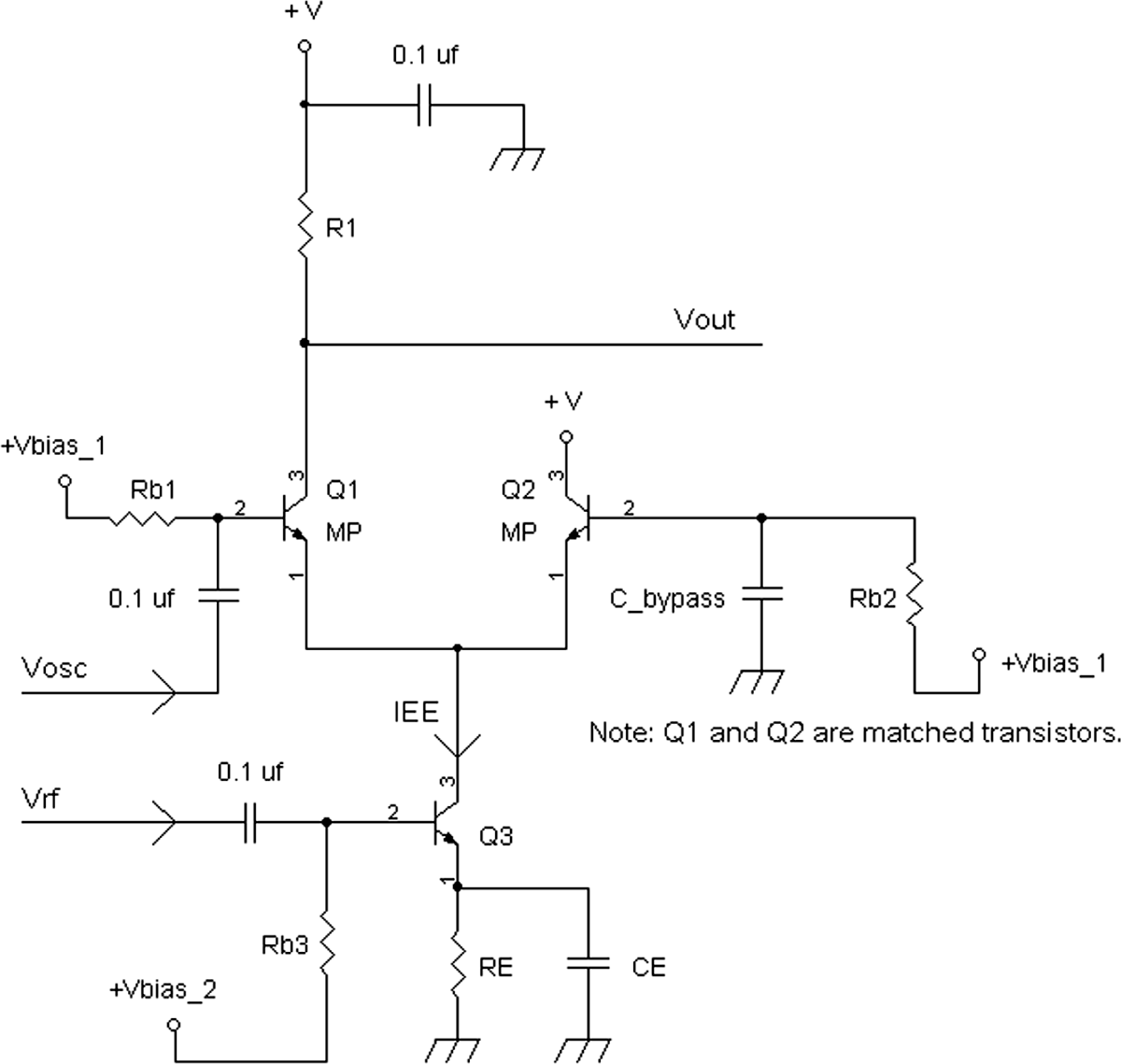
FIGURE 14-8 A differential-pair mixer with three transistors.
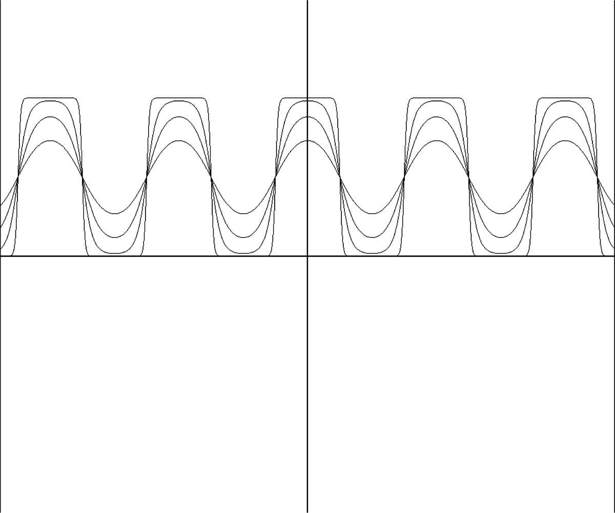
FIGURE 14-9 Q1 collector output for various input sine-wave input levels at 0.026, 0.052, 0.104, and 0.416 V peak. The X axis is time, whereas the Y axis is the amplitude.
With the base of Q2 AC grounded, the collector current from Q1 is
![]()
where IEE is the DC emitter “tail” current, and Isig is the AC signal current for modulating, which means that Isig = gm3 × VRF = IRF sin (2πF2)t.
If VB1 is a sinusoid signal at a frequency of F1 at about 1 volt peak to peak, then the expression

which approximately represents a square-wave signal. And if Isig5 IRF[sin(2μF2)t], then

If the harmonics are ignored, we have
![]()
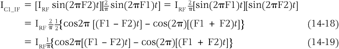
Since the RF signal at frequency F2 and oscillator signal at frequency F1 can be filtered out, let’s just look at the relevant product term related to the IF signal, which is a signal at frequency F1 – F2 or F1 1 F2. Therefore,
And if the RF signal voltage is small, such as less than 10 mV peak,
![]()
where gm3 = IEE/0.026 volt and Vin is the amplitude of the RF signal, then
![]()
The conversion transconductance is gm3(1/p). So, if IEE = 1 mA, then the conversion transconductance is 0.0384/p = 0.0122 mho.
One should note that the square-wave signal from the differential-pair mixer consists of odd harmonics that are attenuated by a factor of 1/N, where N is the odd harmonic. So, for example, the third harmonic is one-third the amplitude of the fundamental frequency and the eleventh harmonic is one-eleventh the amplitude of the fundamental frequency. Therefore, the conversion transconductance for mixing with the harmonic of frequency F1 is just multiplied by a factor of 1/N.
Thus the differential-pair mixer equation (14-16) shows that the RF signal current also multiplies with signals whose frequencies are odd multiples of F1. This then means that mixes with the harmonics of F1 and thus provides harmonic mixing.
Harmonic Mixer Circuits
In the previous two circuits, the one-transistor mixer and differential-pair mixer, we were concerned only with the mixers generating a sum- or difference-frequency signal, with frequency (F1 – F2) or (F1 + F2). But we also have seen that both the single-transistor and differential-pair mixer circuits generate signals with harmonics of the oscillator frequency.
If we define the frequency F1 as FOSC and frequency F2 as FRF, then we can show examples of simple mixing (sum and difference frequencies) and harmonic mixing in Table 14-3.
TABLE 14-3 Out-Frequencies for Simple and Harmonic Mixers

Now let’s return to the one-transistor mixer. We can compare the ratio of conversion transconductance to small-signal transconductance, this time including mixing at harmonics of the oscillator frequency. Table 14-4 shows that the conversion gain for harmonic mixing is almost the same as the conversion gain for simple mixing when the oscillator injection voltage is about 500 mV peak sine wave into the baseemitter junction. However, one downside to having high-amplitude injection voltages into the mixer is that more filtering may be required at the mixer’s output to filter out all the signals of fundamental and harmonic frequencies related to the oscillator frequency.
TABLE 14-4 Transconductance Ratios for a Single-Transistor Mixer
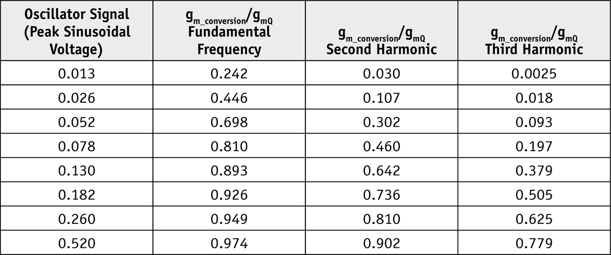
So the bottom line is if harmonic mixing is needed in a one-transistor mixer, make sure that the oscillator voltage is at least 130 mV peak into the base-emitter junction. gm_conversion/gmQ is known from this table and gmQ = ICQ/0.026 volt, gm_conversion can be found. For example, if the oscillator injection voltage is 0.052 V peak into the base-emitter junction, then for the second harmonic of the oscillator signal mixing with the RF signal, we have
![]()
and thus
![]()
If ICQ = 1 mA, then gmQ = 0.0384, and then
![]()
Now let’s take a look at the harmonic conversion transconductance of the differential-pair mixer. For mixing at the fundamental frequency, Equation (14-18) states
![]()
But we can modify this equation for any Nth harmonic by factoring N, which leads to
And this leads to a modification of Equation (14-19):
![]()
And for an Nth harmonic, where N is an odd number, the output signal is
![]()
And thus the conversion transconductance is
![]()
where gm3 = IEE/0.026 volt.
For example, for harmonic mixing based on the fifth harmonic to provide an output signal whose frequencies are 5FOSC ± FRF, the conversion transconductance is
![]()
where g m3 = IEE/0.026 volt the small-signal transconductance of Q3 in Figure 14-9.
Mixer Oscillator Circuits
At this point of writing this chapter I am glad to leave the world of complicated equations. So back to circuits!
In essence, some oscillator circuits can double as a mixer circuit as well. You have seen these circuits in Chapters 8 and 10, and they are called converter circuits. The conversion gain analysis is the same as in the preceding section for a one-transistor mixer. Typically, the self-oscillating voltage is usually set for about 100 mV to 200 mV peak into the base-emitter junction for the converter circuit, so the conversion transconductance for simple mixing will be about the same as the small-signal transconductance.
Figure 14-10 presents a schematic for an oscillator converter circuit. Figure 14-10 shows a common base oscillator that has a low-impedance oscillating voltage fed to the emitter of Q1 via a tap from the oscillator transformer. The base of Q1 is coupled to the RF input signal. It should be noted that the RF signal source should have a low-impedance drive so as to ensure that oscillation occurs reliably. This is why if one inspects the converter circuits in Chapter 8 orChapter 10, the RF signal is stepped down via the secondary winding of the antenna coil. The RF signal’s amplitude should be much smaller than the oscillator’s signal. For example, if the oscillator’s amplitude is 250 mV peak into the base-emitter junction, the RF signal should be under 25 mV peak.
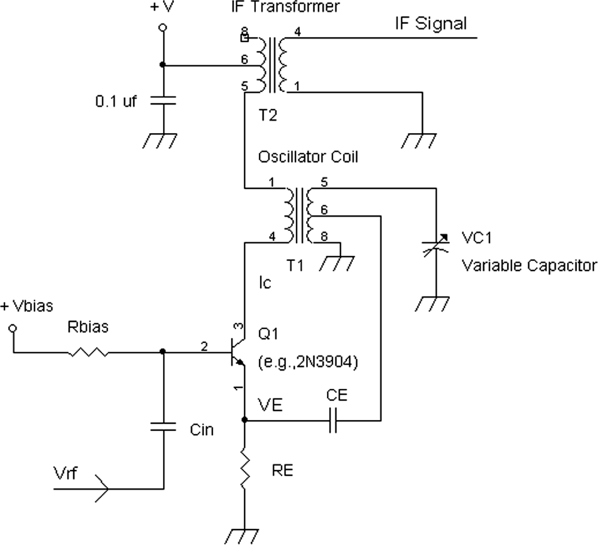
FIGURE 14-10 An oscillator mixer circuit or converter circuit.
Also note that the RF signal’s frequencies should be way beyond the pass band of the oscillator’s tank circuit. For example, if a very low IF is desired, such as 10 kHz, the RF signal itself may cause the oscillator frequency to pull over to the RF frequency. Thus, if the oscillator is set at 1,010 kHz and the incoming RF signal is at 1,000 kHz, there can be a problem of oscillator-frequency stability. Therefore, the RF signals whose frequencies are close to the oscillator’s frequency can cause the oscillator to lock onto or synchronize with the incoming RF signal via injection locking.
Figure 14-10 also can be used as a harmonic converter. If this is desired, the oscillator’s signal should be increased by increasing the DC collector current to provide a “reasonable” conversion gain. This can be done by increasing the bias voltage at the base of Q1 by increasing Vbias and/or by decreasing the resistance of emitter bias resistor RE.
Figure 14-11 shows a differential-pair oscillator with an emitter tail current source that also amplifies the RF signal source. Thus the emitter current is a combination of a DC current and the amplified RF signal current. The IF signal is extracted via the collector of Q2. This is not as common a configuration for a mixer oscillator circuit compared with the one-transistor circuit in Figure 14-10 but nevertheless is workable. Care should be taken as to the RF level connected to the base of Q3.
FIGURE 14-11 A differential-pair oscillator mixer circuit.
If RF gain reduction is needed, an emitter capacitor CE can be replaced with a series capacitor and resistor combination (RC), and the transconductance of Q3 is lowered.
Conversion Gain
Conversion gain is usually the ratio of the voltage amplitudes of the output IF signal to the input RF signal. When the conversion transconductance is known, the conversion gain is just
![]()
where R1 is the equivalent load resistance (usually) in a parallel LC tank circuit. If the mixer’s output current is connected to a tapped transformer, then the turns ratio must be taken into consideration. For example, many IF transformers have a turns ratio of 3:1 in the primary winding. If the IF transformer has an equivalent parallel resistance of 200 k![]() , then the resistance at the low-side tap is (1/32) × 200 k
, then the resistance at the low-side tap is (1/32) × 200 k![]() , or 22.2 k
, or 22.2 k![]() = R1. Also note that the output signal at the secondary winding of the IF transformer will be lower than at the primary winding owing to the step-down ratio.
= R1. Also note that the output signal at the secondary winding of the IF transformer will be lower than at the primary winding owing to the step-down ratio.
Before I end this chapter, I offer Table 14-5, which lists various conversion transconductances of different devices for comparison. For the one-transistor mixer, assume that the driving voltage at the base-emitter junction is above 125 mV peak, which translates to a conversion transconductance of about 90 percent of the small-signal transconductance of a bipolar transistor.
As can be seen in Table 14-5, the two vacuum tubes, 1R5 and 12BE6, which were used in superheterodyne radios, have conversion transconductances very close to that of a bipolar transistor running at a collector current of 10 μA. This fact will give you a hint as to how the ultralow-powered superheterodyne radios of Chapter 9 were designed.
TABLE 14-5 Conversion Transconductances of Transistors, Vacuum Tubes, and MOSFETs

References
1. Class notes EE140, Robert G. Meyer. UC Berkeley, Fall 1975.
2. Class notes EE240, Robert G. Meyer. UC Berkeley, Spring 1976.
3. Paul R. Gray and Robert G. Meyer. Analysis and Design of Analog Integrated Circuits. New York: John Wiley & Sons (any edition).
4. Kenneth K. Clarke and Donald T. Hess. Communication Circuits: Analysis and Design. Reading: Addison-Wesley, 1971.
5. RCA Transistor Thyristor and Diode Manual (Technical Series SC-15), Somerville: RCA Corporation, 1971.
6. Mary P. Dolciani, Simon L. Bergman, and William Wooton. Modern Algebra and Trigonometry. New York: Houghton Mifflin, 1963.
7. William E. Boyce and Richard C. DiPrima. Elementary Differential Equations and Boundary Valued Problems. New York: John Wiley & Sons, 1977.