Chapter 19
Amplifier Circuits
My thought on writing a chapter on amplifiers is that only certain topics about amplification will be explained. There are literally hundreds of books on amplifier design, including operational amplifiers, radio-frequency (RF) amplifiers, low-noise preamplifiers, audio power amplifiers, servo amplifiers, instrumentation amplifiers, and so on. Some of these books cover detailed material concerning input stages, voltage-gain stages, and output stages. And when video amplifiers are covered, a new set of specifications and signals is introduced, such as differential gain and phase, 2T pulse response, color bar, and multiburst signals.
As I am writing this chapter, I know that some readers would like more material on amplifiers. Given the constraints of this book, though, which relates to radio circuits that include audio amplifiers, the following subjects will be covered.
1. Operational amplifiers
2. Basic characteristics of amplifiers, such as gain and frequency response
3. Connecting multiple amplifiers and biasing concerns
4. Practical considerations when using amplifiers
Introduction to Operational Amplifiers
An operational amplifier (or op amp) generally has two input terminals and an output terminal. Of course, there are usually two power-supply terminals as well (Figure 19-1).
For controlled amplification, the op amp must have some type of feedback element from the output terminal to one of the input terminals. The form of feedback must be negative feedback. In some instances, the output terminal is connected to an inverting device such as a common-emitter amplifier or inverting amplifier, which means that the output of the inverting device must be connected to the positive (+) input of the op amp.
However, more commonly, the output of the op amp is connected through a resistor and or capacitor to the negative (-) input of the op amp (Figure 19-2).

FIGURE 19-1 An operational amplifier.
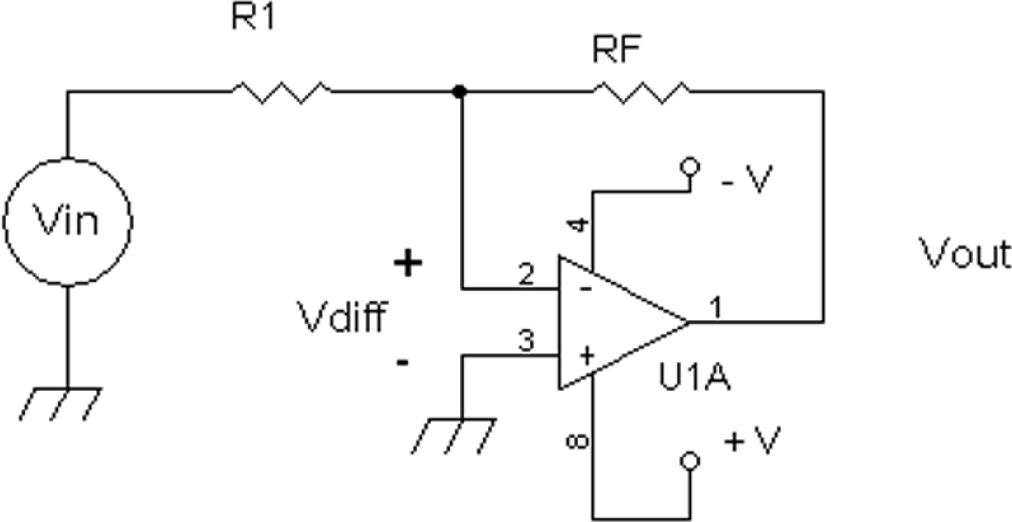
FIGURE 19-2 An op amp configured for inverting gain.
The general rules for analyzing an op amp circuit are as follows:
1. The op amp must have a net negative feedback. That is, if there is both positive and negative feedback from the output to the (–) and (+) inputs, there has to be more negative feedback than positive feedback. In most cases, there are only feedback elements from the output to the (–) input.
2. The raw or open-loop gain of the op amp is very large (>10,000).
3. Once negative feedback is achieved, two conditions hold. One is that the current into the (–) and (+) inputs is zero, and the other is that the potential difference between the two inputs (–) and (+) is zero. That is, the (–) input and the (+) input have the same voltage.
If there is net positive feedback in an op amp circuit, usually there is some combination of oscillation or the output terminal being stuck near one of the power-supply voltages.
In Figure 19-2, the (+) input is grounded, and given feedback resistor RF, there is negative feedback. The voltage at the (+) input is the same voltage at the (–) terminal. This means that the (–) terminal looks like a ground potential. Therefore, to find the gain, or we sum the currents into the (–) terminal to equal 0. That is,
![]()
![]()
![]()
Thus gain is just set by the two resistors RF and R1. Also, because the (–) input is a virtual ground, the input resistance in the view of Vin is just R1 because the (–) input connected to R1 is virtually grounded since the (+) input is grounded.
What the virtual ground at the (–) input also implies is that the input resistance at the (–) terminal is nearly 0 V to ground when there is a negative-feedback resistor connected from the output to the (–) terminal of the op amp and when the open-loop gain of the op amp is very large.
Now let’s take a look at two characteristics of this op amp circuit. One is to establish the input resistance at the (–) terminal with a given negative-feedback resistor RF and a given open-loop gain of the amplifier. And the other is to examine why the voltages are the same for the (–) and (+) inputs when negative feedback is applied.
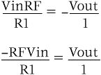
For a negative-feedback amplifier with a feedback resistor RF, Figure 19-3 shows an amplifier with gain –A to mimic the configuration as shown in Figure 19-2. To calculate the input resistance, we need to know
![]()
However, we can equivalently show Figure 19-3 as Figure 19-4. If Vintest = 1 volt DC and –A = –2 and RF 5 1000 ![]() , the voltage at the resistor, RF, is + 1 volt DC on one end and –2 volts DC on the other end of RF, thereby forming 3 volts across RF, or 3 milliamps of drain when 1 volt DC is applied at the input. At first glance, this seems counter intuitive since most of the time we are used to believing the worse case concerning current drain for a resistor is to have one end grounded, which would result in 1 volt across the resistor to yield 1 milliamp of resistor current.
, the voltage at the resistor, RF, is + 1 volt DC on one end and –2 volts DC on the other end of RF, thereby forming 3 volts across RF, or 3 milliamps of drain when 1 volt DC is applied at the input. At first glance, this seems counter intuitive since most of the time we are used to believing the worse case concerning current drain for a resistor is to have one end grounded, which would result in 1 volt across the resistor to yield 1 milliamp of resistor current.
FIGURE 19-3 An amplifier with feedback resistor RF.
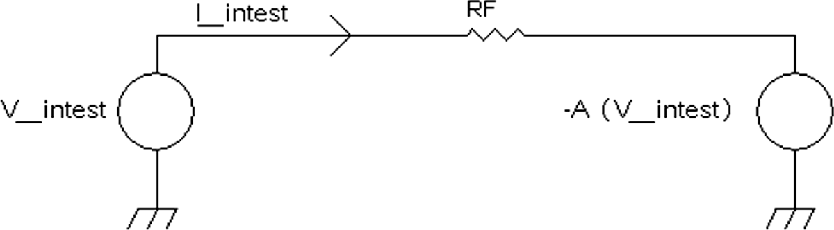
FIGURE 19-4 An equivalent circuit to Figure 19-3 for determining Vin_test/Iin_test.
So what happens if by “magic” we make the amplifier’s gain –A = –1,000,000? With Vintest = 1 volt DC, this would mean that there is 1,000,001 volts across the resistor RF = 1,000 ![]() , so Iintest = 1,000.001 A. And this excessive current would be equivalent to Vintest loading into a resistor of about 0.001
, so Iintest = 1,000.001 A. And this excessive current would be equivalent to Vintest loading into a resistor of about 0.001 ![]() , or for all practical purposes, Vintest is loading into a short circuit.
, or for all practical purposes, Vintest is loading into a short circuit.
Thus the general equation for finding the input current drain with feedback resistor RF in Figure 19-4 is
![]()
![]()
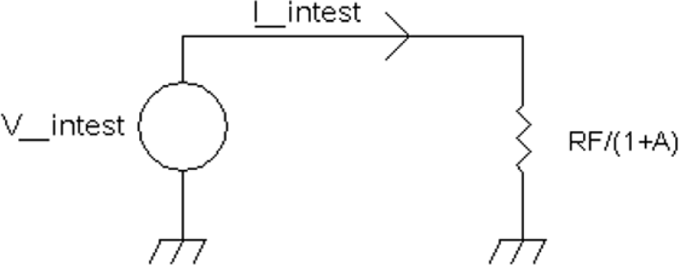
FIGURE 19-5 The equivalent input resistance caused by a feedback resistor and inverting amplifier.
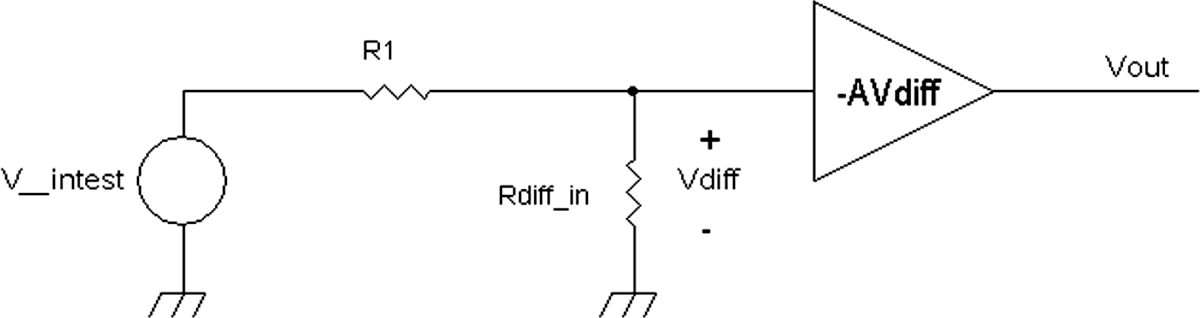
FIGURE 19-6 An equivalent circuit to Figure 19-2.
Thus, if the amplifier’s gain is very large, the input resistance at the (–) input terminal of the op amp approaches a short circuit. Figure 19-5 shows an equivalent input resistance at the input terminal. Another way to model the inverting op amp circuit in Figure 19-2 is via Figure 19-6. In this figure, the input resistor R1 is voltage divided via Rdiff_in = RF/(1 + A) to form the input voltage Vdiff.
![]()
![]()
![]()
![]()
![]()
For large values of A, that is, the op amp has a very large open-loop gain -A/(1 + A) = -1 and RF/(1 + A) = 0, then
![]()
This is the same answer as calculated before. Also note that
![]()
Again, for large values of -A,
![]()
This means for a large open-loop gain, the voltage across the (-) and (+) input terminals, which is Vdiff, goes to zero.
Figure 19-3 showed that when a resistor RF is connected in a negative-feedback configuration of an amplifier whose gain is -A, the equivalent resistance looking into the input of the amplifier is RF/(1 + A). The negative feedback thus causes a “divided” or “reduced” resistance effect by pulling more current at the input of the amplifier than expected.
Now suppose that the resistor RF is replaced with a capacitor CF whose impedance is ZCF = 1 /j2πfCF and the voltage source Vin is replaced with an alternating-current (AC) signal source Vac (Figure 19-7).
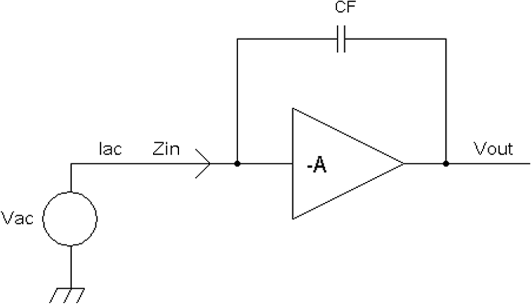
FIGURE 19-7 A Miller capacitance multiplier circuit that uses a feedback capacitor.
j = ![]() , an imaginary number. And impedance, which is measured in ohms, is any combination of resistance and/or reactance, where reactance includes the term j2πf. Resistance is limited to the real numbers, and impedance includes the complex numbers (real and/or imaginary numbers).
, an imaginary number. And impedance, which is measured in ohms, is any combination of resistance and/or reactance, where reactance includes the term j2πf. Resistance is limited to the real numbers, and impedance includes the complex numbers (real and/or imaginary numbers).
We should expect that the negative feedback will cause more current drain at the input, and the AC input impedance is
![]()
Thus the impedance Zin at the input terminal of the amplifier with gain of -A looks like the impedance of a capacitor that has a capacitance of [CF(1 + A)]. Or equivalently, the input to the amplifier with a feedback capacitor CF is capacitive with a capacitance of CF multiplied by (1 + A).
Multiplying capacitance lowers the impedance, which is in accordance with Figures 19-3 and 19-5, which show that a resistive feedback element results in a reduced or lowered resistance at the input of the amplifier. Stated another way, Figure 19-8 shows the equivalent AC voltage across capacitor CF and its AC current Iac.
The AC current is
![]()
After rearranging the equation and noting that ZCF = 1/j2pf CF, the impedance at the input of the amplifier is
![]()
Thus the Miller capacitance is CF(1 + A)], which is the capacitance at the input of the amplifier to ground (see Figure 19-9).
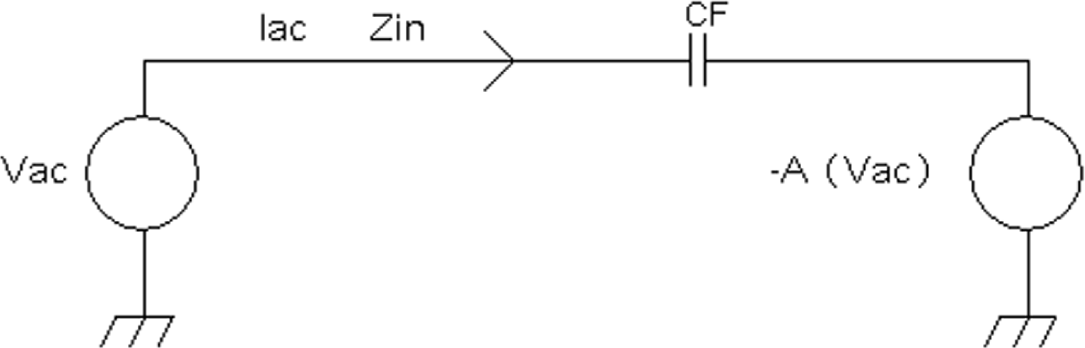
FIGURE 19-8 An equivalent circuit showing the voltage sources across capacitor CF.
In common-emitter amplifiers, the Miller capacitance exists and multiplies the collector-to-base capacitance by (1 + A) where A is the inverting gain from the base to the collector. This Miller capacitance usually robs the amplifer’s high-frequency gain and reduces its input impedance and can be considered a “bad” effect. As shown in Chapter 17, the Miller capacitance can be reduced or eliminated by using a cascode amplifier or a differential amplifier. Another way to reduce the effects of Miller capacitance in a common-emitter amplifier is to connect an emitter follower before the common-emitter amplifier. The emitter follower will be designed to drive the increased capacitance at the input and thus maintain the desired high-frequency response.
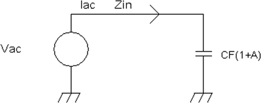
FIGURE 19-9 An equivalent capacitance at the input owing to a feedback capacitor and an inverting amplifier.
In op amps, often there are two voltage-gain stages, and in order to maintain unity-gain stability, the Miller capacitance is often used. The second stage usually includes extra capacitance across the base and collector of a common-emitter amplifier for a deliberate high-frequency roll-off to the overall open-loop gain of the op amp such that when negative feedback is applied, there are no oscillations.

FIGURE 19-10 A noninverting amplifier with feedback resistors RF and R1.
Now a noninverting op amp circuit will be examined (Figure 19-10). In analyzing the inverting amplifier of Figure 19-2, when the open-loop gain A is large, the voltage at the (–) and (+) terminals of the amplifier is the same. Therefore, the voltage at the (–) terminal in Figure 19-10 is Vout[R1/(R1 + RF)], and the voltage at the (+) input terminal is just Vin. Therefore,
![]()
or
![]()
which leads to
![]()
However, if the open-loop gain A is just some gain value, then Vout/Vin can be determined as a function of A. See Figure 19-10.
![]()
![]()
![]()
![]()
![]()
![]()
![]()
![]()
![]()
Now let’s check the equation. If R1 = 0, then we should have just the open-loop gain
![]()
In reality, if R1 is shorted to ground, the output of the op amp will head toward one of the power-supply rails. And if A is very large such that (A + 1)R1 >> RF, we will get
![]()
Amplifier Characteristics
In this section, only two topics will be covered. One is the input resistance to a common-emitter amplifier with an emitter resistor when the emitter is not AC grounded. The other is the gain of the common-emitter amplifier with this emitter resistor.
While there are plenty of other topics that can be covered, there are many excellent books on op amp applications and transistor amplifiers. Two of them that come to mind are
1. Intuitive IC Op Amps from Basics to Useful Applications, by Thomas M. Frederiksen (National’s Semiconductor Technology Series, Santa Clara: National Semiconductor Corporation,1984).
2. Bipolar and MOS Analog Circuit Design, by Alan B. Grebene, New York: John Wiley & Sons (1984).
The reader can consult these books for much more detail on amplifiers in general.
Figure 19-11 shows a simple common-emitter amplifier with an emitter resistor RE. Note that there is no capacitor from the emitter of Q1 to ground.
Analyzing the common-emitter amplifier in Figure 19-11 will be done a little bit differently from most college courses that use hybrid π transistor models. Instead, some simple equations will be used.
Recall the following if the transistor’s current gain β is large: The output resistance looking into the emitter with the base connected to a voltage source is 1/gm, which is equal to the output resistance of an emitter follower when the base is driven by a low-source-resistance signal voltage.
![]()
![]()
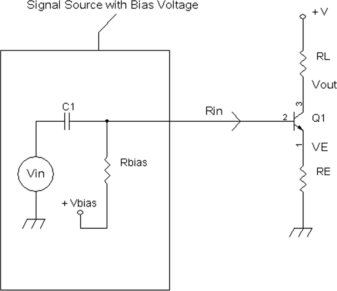
FIGURE 19-11 Common-emitter amplifier with a local negative-feedback resistor RE.
where ICQ = quiescent collector DC current.
Now referring to Figure 19-11, one will see that Vin = VBE + VE. Therefore the AC signals can be characterized as:
![]()
To find the input resistance, we need to find
![]()
Therefore,
![]()
But we know that the voltage at the emitter is VE = (IE)RE. Therefore, the change in emitter voltage VE over the change in emitter current is RE.
![]()
and that IE = (β + 1)IB. Therefore, ΔIE = (β + 1)ΔIB, and
![]()
which then leads to
![]()
by substitutions,
![]()
The emitter resistor can have beneficial effects in terms of raising the input resistance. For example, if ICQ = 26 mA, β = 100, and RE = 0, β/gm = 100 ![]() , and Rin = (100 + 0) μ, a low input resistance. However, if RE is 10 ohms, then (β + 1)RE = (101)10
, and Rin = (100 + 0) μ, a low input resistance. However, if RE is 10 ohms, then (β + 1)RE = (101)10 ![]() = 1,010
= 1,010 ![]() , and Rin = (100 + 1,010)
, and Rin = (100 + 1,010) ![]() = 1,110
= 1,110 ![]() , a medium input resistance. Of course, having RE at 10
, a medium input resistance. Of course, having RE at 10 ![]() also reduces the overall transconductance of the transistor, as we will see in the following analysis.
also reduces the overall transconductance of the transistor, as we will see in the following analysis.
Transconductance of the transistor is given by
![]()
When there is an emitter resistor as shown in Figure 19-11, we define a new transconductance, g~m, as:
![]()
For large β, ΔIE = ΔIc.
The AC emitter current is
![]()
However, the AC voltage at the emitter has to take into account the output resistance 1/gm of the emitter follower. The emitter then provides the input AC signal ΔVin with a series resistance of 1/gm to drive into resistor RE. As a result, a voltage divider is formed, and the AC voltage at RE is ΔVE:
![]()
![]()
![]()
By substitution,
![]()
and dividing RE from both sides of the equation gives
![]()
which leads to
and multiplying by gm at the numerator and denominator,
![]()
or alternatively and probably more useful to do quick calculations is:
![]()
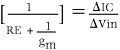
Thus the emitter resistor reduces or scales the original transistor’s transconductance by a factor of
![]()
For example, with 26 mA of collector current, gm = 1 mho, and with RE = 10 ![]() , then
, then
![]()
Therefore, in this particular example, the “penalty” of having a 10-![]() emitter feedback resistor is a reduction in the transistor’s transconductance by 11-fold. This reduction in transconductance means that the gain of the amplifier will be reduced 11-fold. But the “bright” side is that the input resistance in this example had increased about 11-fold. Also, the linearity of the amplifier with the 10-
emitter feedback resistor is a reduction in the transistor’s transconductance by 11-fold. This reduction in transconductance means that the gain of the amplifier will be reduced 11-fold. But the “bright” side is that the input resistance in this example had increased about 11-fold. Also, the linearity of the amplifier with the 10-![]() emitter resistor increased dramatically, and thus having the emitter resistor also reduces distortion for the same output voltage.
emitter resistor increased dramatically, and thus having the emitter resistor also reduces distortion for the same output voltage.
Another advantage is the output resistance from collector to ground for this example is increased by about 11-fold given the 10-![]() emitter resistor. For example, given an Early voltage of 100 volts at 26 mA, the collector-to-emitter resistance is about 3.84 k
emitter resistor. For example, given an Early voltage of 100 volts at 26 mA, the collector-to-emitter resistance is about 3.84 k![]() . If the emitter is grounded via a large emitter capacitor to ground, the circuit has an internal 3.84-k
. If the emitter is grounded via a large emitter capacitor to ground, the circuit has an internal 3.84-k![]() resistor in parallel with the collector load resistor. However, if RE = 10
resistor in parallel with the collector load resistor. However, if RE = 10 ![]() , the equivalent output resistance from collector to ground is now 11 times larger, or 42.3 k
, the equivalent output resistance from collector to ground is now 11 times larger, or 42.3 k![]() . And thus the collector load resistor will be in parallel with a 42.3-k
. And thus the collector load resistor will be in parallel with a 42.3-k![]() resistor instead of a 3.84-k
resistor instead of a 3.84-k![]() resistor.
resistor.
Before we leave this section, here is an intuitive explanation of why an emitter resistor raises the output resistance of the transistor. See Figure 19-12 with internal resistor r0. When the emitter of Q1 is grounded, by inspection, the lossy or extra resistance is r0 from the collector to ground. However, with an emitter resistor RE, let’s examine what happens when the supply voltage is raised. The collector-to-emitter resistor r0 actually adds current to the emitter of the transistor to partially reduce the base-to-emitter voltage. So, as the voltage is increased at the collector, the transistor’s emitter receives a current via r0 to slightly lessen the base emitter voltage and thus cause the collector current to reduce. The total collector current, including the current flow into r0, then is stabilized and does not increase as much compared with the emitter being grounded.
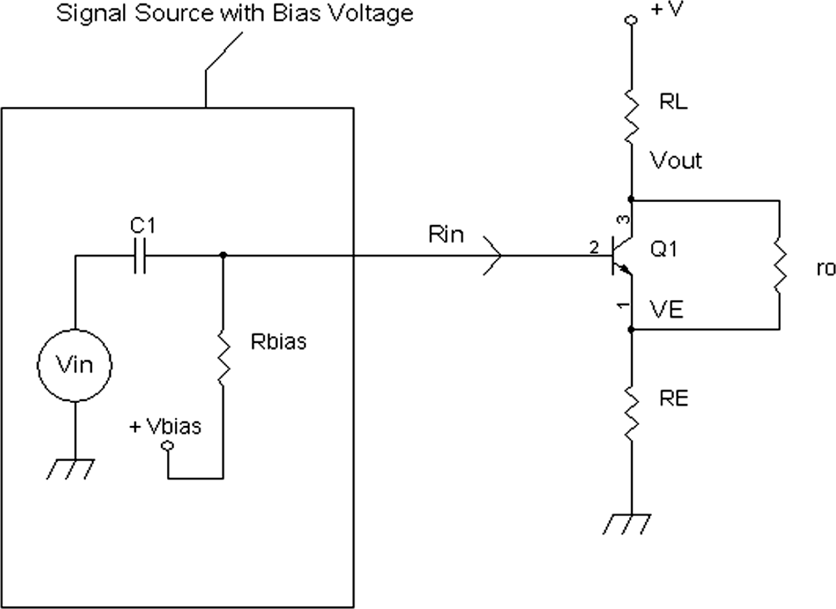
FIGURE 19-12 Common emitter amplifier with internal resistor.
Connecting Multiple Amplifiers for an Amplifier System
Often a single-stage amplifier or single-transistor amplifier may not provide enough gain, or high enough input resistance, or power output into a low-resistance load. Therefore, multiple transistor stages are required. In other cases, although the amplifier’s gain may meet the requirements, the harmonic distortion may be too high or the high-frequency response is inadequate.
For example, in terms of a distortion specification, suppose that a high-gain amplifier of 1,000 is needed for low levels of audio signals that do not exceed 2 millivolts peak with less than 1 percent distortion second harmonic distortion for a sine-wave input signal. Assume a 12-volt power supply with resistive loads and an input resistance greater than 10,000 ![]() , output resistance of 1,000
, output resistance of 1,000 ![]() , minimum output swing of 2 volts peak to peak into an open circuit, and the current gain β = 100 for each transistor. Also assume that the transistors (e.g., MPSH10) have very low capacitance such that the audio-frequency response is not a problem and that there is no Early effect. Also, Vbias = 1.6 volts, and the VBE turn on voltage = 0.6 volt.
, minimum output swing of 2 volts peak to peak into an open circuit, and the current gain β = 100 for each transistor. Also assume that the transistors (e.g., MPSH10) have very low capacitance such that the audio-frequency response is not a problem and that there is no Early effect. Also, Vbias = 1.6 volts, and the VBE turn on voltage = 0.6 volt.
A first try is a common-emitter amplifier, as shown in Figure 19-13. The second-harmonic distortion for a common-emitter amplifier where the emitter is AC grounded via capacitor CE is about 1%/1 mV peak sine-wave input.
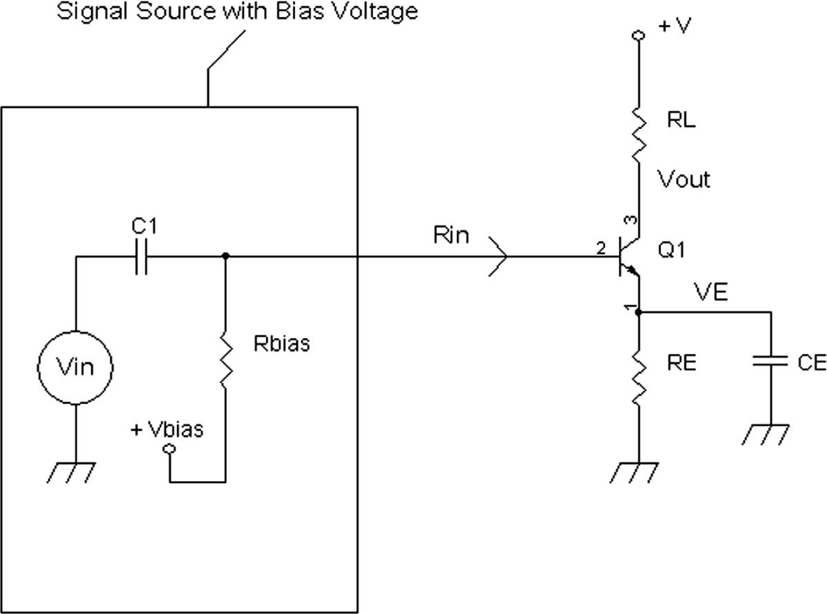
FIGURE 19-13 Common emitter amplifier with an AC-grounded emitter.
Since, the specification is less than 1 percent second harmonic distortion (second harmonic distortion = HD2), this means that the AC-grounded emitter amplifier cannot have an input level of less than 1 mV peak. However, the specification calls for a 2-mV input, which then would result in 2 percent second-harmonic distortion.
If there is an emitter resistor in the common-emitter amplifier and the emitter is not AC grounded, the second-harmonic distortion as a function of input voltage is approximately
![]()
See Figure 19-11. For example, if gmRE = 2, then (1 + gmRE)2 = (1 + 2)2 = 9, and then the second harmonic distortion is
![]()
This would mean with a 2-millivolt peak sine-wave signal at the input would result in less than 1 percent second-harmonic distortion. Note that second-harmonic distortion is in proportion to input voltage, so the expected second-harmonic distortion at the output of the common-emitter amplifier is
![]()
The input resistance into the base amplifier is greater than 10 k![]() . One can precisely calculate the collector current and the associated value of RE. However, in practice, it is easier to just make an estimate. If the collector current is 1 mA, the input resistance is
. One can precisely calculate the collector current and the associated value of RE. However, in practice, it is easier to just make an estimate. If the collector current is 1 mA, the input resistance is
![]()
But RE = 2/gm = 52 ![]() , so
, so
![]()
Let the collector current now equal 0.7 mA; then RE = 74 ![]() and
and
![]()
The load resistor RL gain of the common-emitter amplifier thus is
![]()
If we want a gain of 1,000, RL = 111 k![]() . However, the DC collector current is 0.7 mA, which would develop a voltage of 0.7 mA × 111 k
. However, the DC collector current is 0.7 mA, which would develop a voltage of 0.7 mA × 111 k![]() = 77 volts, which exceeds the 12-volt supply. Therefore, we have to design this amplifier with more than one stage.
= 77 volts, which exceeds the 12-volt supply. Therefore, we have to design this amplifier with more than one stage.
At this point, let’s just make the first stage have a gain of 100 instead and then follow up with a second voltage-gain stage of 10 to provide a total gain of 1,000. Thus RL = 11.1 k![]() for a gain of -100, and the voltage drop across the 11.1-k
for a gain of -100, and the voltage drop across the 11.1-k![]() resistor is 7.7 volts.
resistor is 7.7 volts.
Figure 19-14 shows a practical implementation of setting RE to 74 ![]() . Note in practice the use of a 75-
. Note in practice the use of a 75-![]() resistor. When Vbias is set to 1.6 volts, the base voltage of Q1 is 1.6 volts DC, and the emitter voltage is about 1.0 volt. Thus REQ1 = 1,400
resistor. When Vbias is set to 1.6 volts, the base voltage of Q1 is 1.6 volts DC, and the emitter voltage is about 1.0 volt. Thus REQ1 = 1,400 ![]() will provide a collector current of about 0.7 mA. With a RL = 11.1 k
will provide a collector current of about 0.7 mA. With a RL = 11.1 k![]() (note that the nearest 1 percent value for an 11.1-k
(note that the nearest 1 percent value for an 11.1-k![]() resistor is 11.0 k
resistor is 11.0 k![]() ), this means that the output resistance of the common-emitter amplifier is also 11.1 k
), this means that the output resistance of the common-emitter amplifier is also 11.1 k![]() . Therefore, the gain from the base of Q1 to the collector of Q1 is about -100. Note that capacitor CE in Figure 19-14 has sufficiently large capacitance to provide a short-circuit impedance at audio frequencies.
. Therefore, the gain from the base of Q1 to the collector of Q1 is about -100. Note that capacitor CE in Figure 19-14 has sufficiently large capacitance to provide a short-circuit impedance at audio frequencies.
To minimize further loading effects on RL, an emitter follower buffers this common-emitter amplifier, and the output of the common-emitter amplifier is fed to a second common-emitter amplifier with a gain of about -10 (see Figure 19-15).
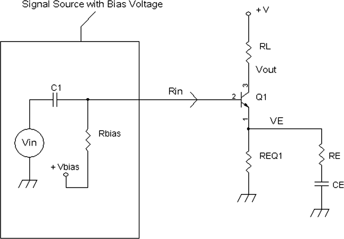
FIGURE 19-14 An input amplifier stage.
When multiple-stage amplifiers are coupled in the manner shown in Figure 19-15, usually the later stages will generate the most distortion. So it is usually preferred to ensure that the first stage’s distortion characteristic is well below the specification (e.g., 0.22 % << 1 %).
The base of emitter follower Q2 is connected to the output of Q1 via RLQ1. The output of the emitter follower then is connected to the base of Q3. Because there is a 7.7-volt drop across the load resistor RL, with a 12-volt supply the DC voltage at the collector of Q1 is 4.3 volts, and the emitter of Q2 is 3.7 volts, which leads to Q3’s emitter voltage of 3.1 volts. Since the voltage swing at the output has to be 2 volts peak, the Q3 collector current will be set for 4 milliamps so that the maximum output swing is about 4 volts peak. However, at 4 volts peak, the distortion is likely to exceed 1 percent. Therefore, half the maximum voltage swing at the collector of Q3 gives a good chance that the distortion specification will be met.
Therefore, REQ3 = 775 ![]() such that 3.1 volts/775
such that 3.1 volts/775 ![]() = 4 mA. For the 1,000-
= 4 mA. For the 1,000-![]() output resistance specification, RLQ3 = 1,000
output resistance specification, RLQ3 = 1,000 ![]() . For a gain of -10, the parallel combination of REQ3 and RE3 must equal about 96
. For a gain of -10, the parallel combination of REQ3 and RE3 must equal about 96 ![]() . Thus RE3 = 110
. Thus RE3 = 110 ![]() .
.
The emitter resistor of Q2 is 5.1 k![]() , and the input resistance to Q3 is about (β + 1)96
, and the input resistance to Q3 is about (β + 1)96 ![]() = 9.69 k
= 9.69 k![]() . Thus the total load resistance at the emitter of Q2 is 5.1 k
. Thus the total load resistance at the emitter of Q2 is 5.1 k![]() parallel to 9.69 k
parallel to 9.69 k![]() = 3.3 k
= 3.3 k![]() . For the current gain (β = 100, the approximate input resistance into the base of Q2 is about (β + 1)3.3 k
. For the current gain (β = 100, the approximate input resistance into the base of Q2 is about (β + 1)3.3 k![]() = 333 k
= 333 k![]() . Because the output resistance of first stage is about 11.1 k
. Because the output resistance of first stage is about 11.1 k![]() , the 333-k
, the 333-k![]() load at the base of Q2 provides a negligible effect on the signal amplitude from the collector of Q1.
load at the base of Q2 provides a negligible effect on the signal amplitude from the collector of Q1.
So now let’s calculate the distortion at Q3. The gain from Q1 and unity-gain amplifier Q2 is 100, which means that for a 2-mV peak input signal, there is a 200-mV peak signal at the emitter of Q2 and base of Q3. The equivalent emitter resistor is RE_equiv = 96 ![]() , the parallel combination of the two emitter resistors REQ3 and RE3 connected to Q3. At 4 mA, gm_Q3 = 0.1536 mho.
, the parallel combination of the two emitter resistors REQ3 and RE3 connected to Q3. At 4 mA, gm_Q3 = 0.1536 mho.
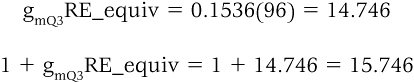
and thus the distortion from Q3’s output is

Since 200 millivolts peak is less than 247 millivolts, the output of Q3 will have less than 1 percent second order harmonic distortion. And since the second harmonic distortion is proportional to the input level, the expected second harmonic distortion is
![]()
Actually, there may or may not be a bit more because there is about 0.22 percent distortion from Q1, but the total distortion rarely adds in a linear fashion from all the amplifier stages. The amplifier was built and with a 2 mV peak sinusoidal waveform at its input, the second harmonic distortion was measured at about 0.65 percent. It appears that the second harmonic distortions of the first and third stages partially cancel instead of adding. Intuitively, the partial cancellation makes sense. As the first stage is increasing in Q1’s collector current, which increases the transconductance of the first stage, the output voltage from the first stage is lowered that causes the collector current of the third stage to lower. This in turn causes the transconductance of the third stage to lower as well. Therefore, the combination of increasing and decreasing transconductances of the first and third stages result in a more constant transconductance, which then increases linearity of the combined amplifying stages.
The distortion can be lowered further just by increasing the collector current of Q3 from 4 mA to 5 mA, which will reduce the distortion of the Q3 amplifier by about 35 percent further to about 0.52 percent second harmonic distortion.
Thus, Figure 19-15 is just one example of designing an amplifier or amplifier system consisting of multiple stages of amplification. This example was chosen to show the interaction of input resistance, output resistance, gain, and distortion considerations in designing an amplifier. Obviously, there are other parameters one must take into account, such as power consumption, sensitivity to power-supply noise, small- and large-frequency response, cost, and board space, to name a few.

FIGURE 19-15 A three-stage amplifier.
Practical Considerations for Using Amplifiers
In Chapter 18 concerning automatic volume control (AVC) amplifiers, it was shown that for a common-emitter amplifier, a minimum base voltage is required for turning on the transistor for amplification. In op amps, one must consider the minimum voltage needed to bias on the transistors for amplification. This section will cover biasing conditions, output swing, and frequency response of op amps.
Figure 19-16 shows basically two types of input stages. One important consideration for using op amps is determining the voltage range at the input terminals that allows proper biasing within the op amp. This voltage range is named the common-mode input voltage, which is based on a given supply voltage. For now, assume that the –V supply voltage is grounded.
In Figure 19-16, the NPN differential amplifier input stage consisting of Q1 and Q2 has an emitter current source Q3. This type of input stage can be found in the NE5534 op amp. Generally, for each transistor allow 0.7 volt minimum for VBE base-to-emitter turn-on voltage, and allow the collector-to-base voltage to be generally 0 volt or higher. Therefore when the negative power supply volt is grounded such that –V = 0 volt, the minimum input voltage is at least or equal to 0.7 volt from the VBE base-to-emitter turn-on voltage of f Q1 or Q2 plus another 0.7 volt from the collector Q3. So the minimum voltage at the input terminal is at least 1.4 volts. However, to be on the safe side, the minimum input voltage should be about 2 volts, which is about 1 VBE drop extra to guarantee operation over low temperature.
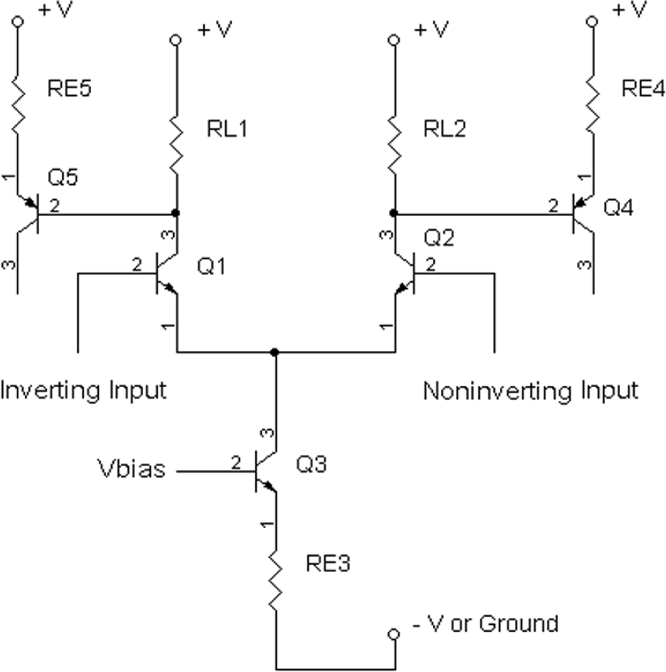
FIGURE 19-16 An op amp input stage using NPN transistors.
For the maximum voltage at the input, the current source provides a voltage drop across the load resistors RL1 and RL2 for Q1 and Q2. If the input voltage is raised too high, the base collector junctions of Q1 or Q2 will forward bias, which will cause Q1 or Q2 to saturate. Therefore, in this example, the input voltage has to be smaller than + V, the supply voltage. The NE5534 specification sheet shows that there must be an input voltage of at least 2 volts below the positive supply voltage or + V –2 volts.
Figure 19-17 shows an LM358 op amp input stage using PNP devices Q1 to Q4. A current mirror active-load circuit is provided by NPN transistors Q5 and Q6. The PNP devices allow the input range to ground or even a little bit below ground, such as –0.5 volt. Q1 and Q2 are PNP emitter follower circuits that level shift the input signal up by about +0.6 volt into the differential voltage gain amplifier Q3 and Q4. The emitter voltage of Q3 and Q4 is about 1.2 volts, which is about 0.6 volt higher than the emitter voltages of Q1 and Q2. This means that the collectors of Q3 and Q4 can operate safely at about +0.6 volt. Note that Q5 with its diode connection provides 0.6 volt at the collector of Q3. The collector of Q4 is allowed to swing from 0 volt to almost 1.2 volts, but normally operates at about 0.6 volt. Thus, the common input voltage for this example works down to 0 volt or to about –0.5 volt.
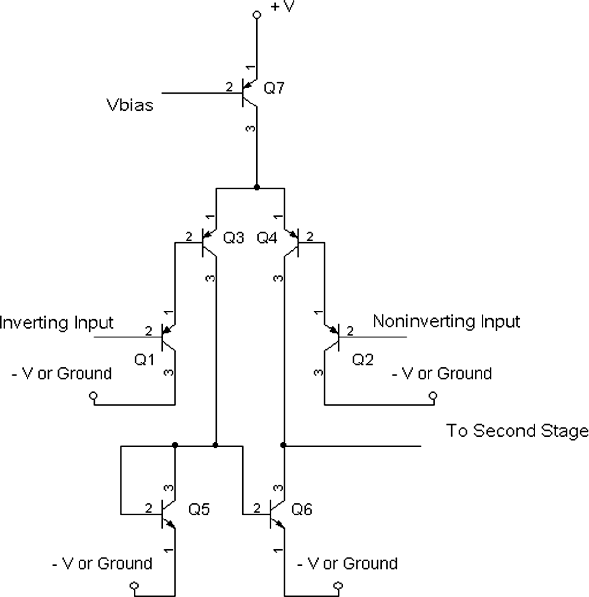
FIGURE 19-17 An op amp input stage using PNP transistors.
In terms of the input voltage near the +V supply, the emitters of Q3 and Q4 are connected to a PNP current source Q7. So the input voltage is level-shifted by 1.2 volts up to the collector of the PNP current source Q7. If the current source allows its collector to still operate correctly at about 0.2 volt below +V, then the positive or high input range about +V – (VBEQ1 + VBEQ3 + 0.2 volt) = +V – 1.4 volts. The LM358 specification sheet states the high input range if +V – 1.5 volts.
Input range becomes important especially when working with a single supply. If an NE5532 is used with a single supply, then the inputs should be biased to about one-half the supply voltage, and the input range has to be 2 volts below the supply voltage and 2 volts above ground. For an LM358, the inputs can be biased at half or slightly lower than half the supply voltage, and the input range will work at 1.5 volts below the (+) power-supply voltage to 0 volt.
It should be noted that the voltage at the (+) input terminal is the one that determines the voltage at the (–) input terminal of the op amp. In terms of op amp output stages, Figure 19-18 shows a typical push-pull output stage using NPN and PNP output transistors. The figure shows an output stage with push-pull emitter followers Q10 and Q11. The maximum output signal then is on the order of a base-emitter turn on voltage plus the saturation voltage of the transistors driving the bases of Q10 and Q11, which is about 0.2 volt. The output-transitor base emitter turn-on voltage is about 0.7 volt. Thus the “loss” is about 0.7 volt plus the loss of 0.2 volt for positive and negative swings of transistors Q12 and Q9, respectively. This results in a maximum high output voltage of about +V –0.9 volt and the low-side voltage is about 0.9 volt from ground. The specification sheet states that the output swing loses about 1 volt for the high-side output and the low-side output.
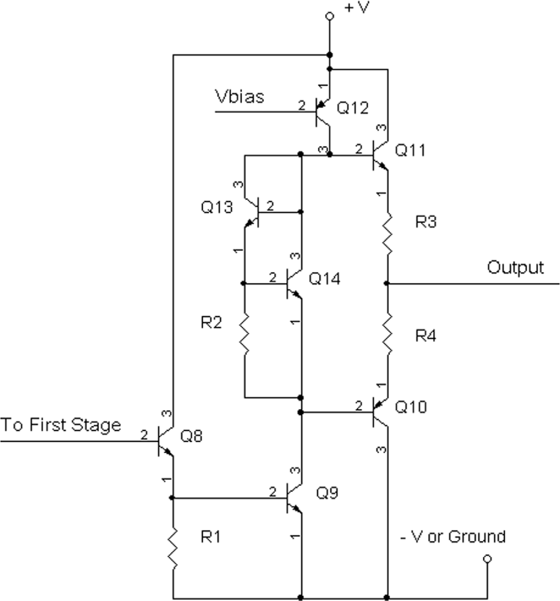
FIGURE 19-18 An RC4558 op amp output stage.
Fortunately, today there are many op amps that will have rail-to-rail output capability, such as the ISL28208 and ISL28218. Also, op amps such as the THS4281 and LM6152 have both rail-to-rail input and output capability.
Now we shall turn to frequency-response considerations in op amps. Op amps are generally unity-gain stable. That is, the op amp can be configured for a unity-gain follower for a gain of +1 without oscillations. Normally, the voltage follower is configured as shown in Figure 19-19.
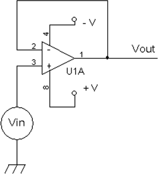
FIGURE 19-19 Op amp configured as a unity-gain voltage follower amplifier.
Most op amps also are specified with a gain-bandwidth product (GBWP). Alternatively, the unity-gain bandwidth is the gain-bandwidth product. For example, if the gain-bandwidth product is 50 MHz, at a gain of +1, the frequency response would be flat and exhibit a –3 dB loss or a drop in gain to 0.707 at 50 MHz. If the gain of the op amp is set for 100, the response will be flat, and at 500 kHz, there will be a drop in gain to 70.7 (see Figure 19-20).
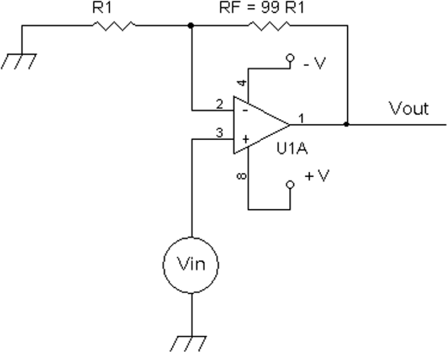
FIGURE 19-20 A noninverting-gain op amp set for 100.
Figure 19-21 illustrates setting a gain of 100 for a single supply. This figure shows a single-supply implementation for an AC gain of +100. R1, which normally goes to ground, is coupled to ground via a capacitor C2. The (+) input of the op amp is biased to one-half the supply voltage, and the AC input signal is coupled to the (+) input via input capacitor C1. The output of the op amp can be coupled to another op amp stage, as in Figure 19-21, because the DC voltage at the output is one-half the supply voltage. Otherwise, the output of the op amp might require an output capacitor C3.
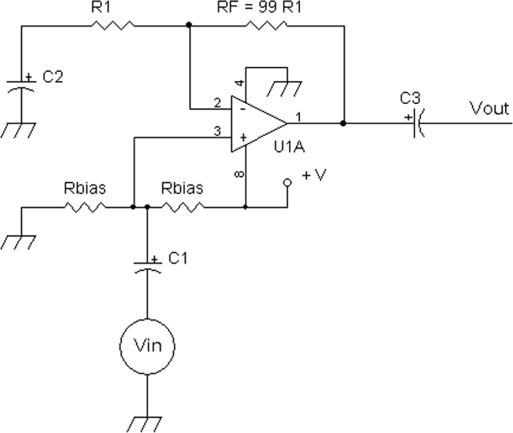
FIGURE 19-21 A single-supply implementation for a gain of +100.
Strictly speaking, the frequency response and gain are not always tied to the gain-bandwidth product. Rather, the frequency response is related to how the negative-feedback network is applied.
where OLBW is the open-loop bandwidth, and OLGain is the open-loop gain at DC.
When a resistive negative-feedback network is connected between the output and the (–) input of the op amp, the bandwidth or –3-dB frequency response in a feedback system is
![]()
FBNet is the resistive attenuation factor from the output to the (–) input.
Figure 19-22 shows a resistive network for an inverting amplifier. The attenuation factor then is R1/(RF 1 R1), and thus the bandwidth of the inverting amplifier is
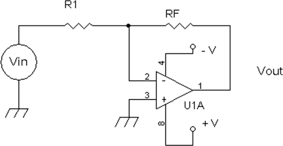
FIGURE 19-22 An inverting amplifier with feedback resistor RF and R1.
![]()
However, usually the OLBW << GBWP[R1/(RF + R1)]. So, commonly, the bandwidth is expressed as GBWP[R1/(RF + R1)] = bandwidth. For example, for a unity inverting gain amplifier, RF = R1, and
![]()
Note that even though the gain is –1, the bandwidth is half the voltage follower.
Now let’s look at an inverting summing amplifier, where all the resistors are equal RF = R1 = R2 = · · · = RN (see Figure 19-23). The attenuation factor from the output to the input is
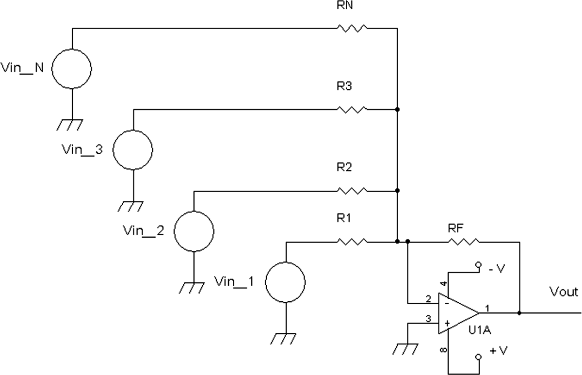
FIGURE 19-23 An N-input inverting summing amplifier.
![]()
because when all the input sources are 0 or grounded, all the resistors from R1 to RN are paralleled, which is the resistance (R1/N).
Therefore,
![]()
So, if N = 100, then there are 100 inputs to the inverting summing amplifier, and the bandwidth is 1/101 of the gain-bandwidth product. For example, if the op amp’s GBWP is 1 MHz and there are 100 inputs with all resistors equal, then the bandwidth is 9.9 kHz, and the gain is –1 for any input.
One can look at the preceding problem another way: if we ground 99 of the inputs and feed R1 with the input signal. The input resistors R2 to R100 are parallel and go to ground. Thus the inverting summer is redrawn in Figure 19-24. For simplicity of analysis, let all resistors have a resistance R. There is a voltage divider from the input side of R and R/99. This resistive divider can be simplified with a Thevenin equivalent circuit, which states that the Thevenin resistance is just the resistance across the resistor going ground, R/99, in parallel with the driving resistance R (see Figure 19-25).
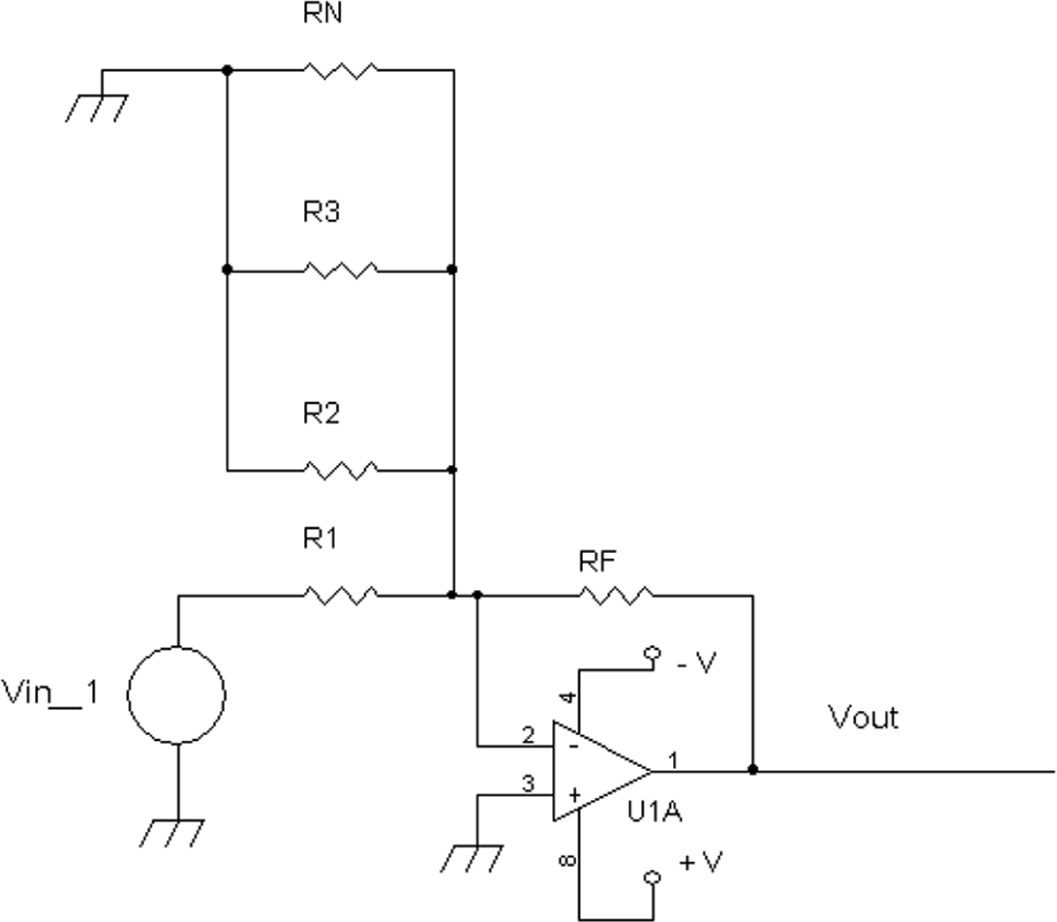
FIGURE 19-24 An inverting summing amplifier redrawn with other inputs grounded.
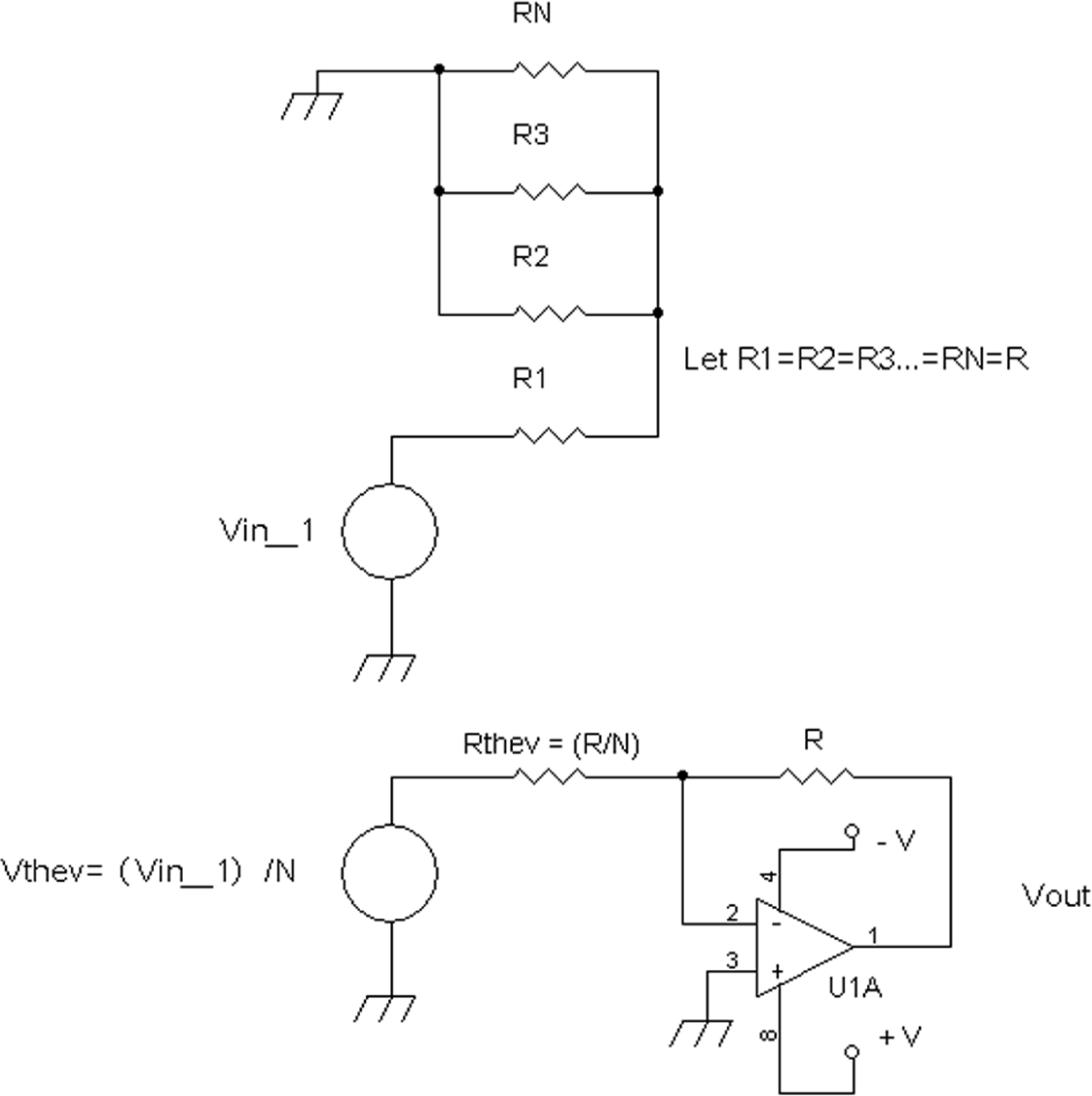
FIGURE 19-25 A Thevenin equivalent circuit to model the summing amplifier with N input resistors.
Therefore, with N = 100, the Thevenin resistance is R/100. And the Thevevin voltage is just the divided voltage times the input voltage. So the Thevenin voltage is
![]()
To calculate the gain Vout/Vin,
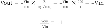
which is expected. However, the attenuation factor is

and thus
![]()
which agrees with the previous analysis. Also note that using the Thevenin equivalent voltage shows that the Thevenin voltage source Vin/100 is being amplified by 100 because the Thevenin resistor, which is the input resistor, is 1/100 of the feedback resistor. By using the Thevenin circuit, the original input signal is attenuated by 100, but that attenuated input signal is being amplified by 100 via the feedback resistor and the Thevenin resistor. So the amplifier is really providing an inverted gain of -100, which accounts for the loss in bandwidth.
To reiterate, though, with a resistive negative-feedback network,
![]()
This makes sense because when R1 = 0, the (-) input is shorted or tied to ground, and there is no feedback; thus the bandwidth is just the open-loop bandwidth OLBW.
In op amps, a DC offset voltage at the output is caused by the input bias currents flowing through the resistors connected to the (+) and (-) inputs. More details of input offset voltages and input current bias effects can be found in Section 3.5 of Thomas M. Frederiksen’s book, Intuitive IC Op Amps (Santa Clara: National Semiconductor Corporation, 1984). However, using an op amp with a field-effect transistor (FET) input stage will eliminate concerns of input bias currents causing offset voltages.
References
1. Class Notes EE141, Paul R. Gray and Robert G. Meyer, UC Berkeley, Spring 1975.
2. Class Notes EE241, Paul R. Gray and Robert G. Meyer, UC Berkeley, Fall 1975.
3. Class Notes EE140, Robert G. Meyer, UC Berkeley, Fall 1975.
4. Class Notes EE240, Robert G. Meyer, UC Berkeley, Spring 1976.
5. Paul R. Gray and Robert G. Meyer, Analysis and Design of Analog Integrated Circuits, 3rd ed. New York: John Wiley & Sons, 1993.
6. Kenneth K. Clarke and Donald T. Hess, Communication Circuits: Analysis and Design. Reading: Addison-Wesley, 1971.
7. Robert L. Shrader, Electronic Communication, 6th ed. New York: Glencoe/McGraw-Hill, 1991.
8. William G. Oldham and Steven E. Schwarz, An Introduction to Electronics. New York: Holt Reinhart Winston, 1972.
9. Allan R. Hambley, Electrical Engineering Principles and Applications, 2nd ed. Upper Saddle River: Prentice Hall, 2002.
10. Gene F. Franklin, J. David Powell, and Abbas Emami-Naeini, Feedback Control of Dynamic Systems, 3rd ed. Reading: Addison-Wesley, 1995.
11. Texas Instruments, Linear Circuits Amplifiers, Comparators, and Special Functions, Data Book 1. Dallas: Texas Instruments Incorporated, 1989.
12. Motorola Semiconductor Products, Inc., Linear Integrated Circuits, Vol. 6, Series B., 1976.
13. Thomas M. Frederiksen, Intuitive IC Op Amps From Basics to Useful Applications (National Semiconductor Technology Series). Santa Clara: National Semiconductor Corporation, 1984.
14. Alan B. Grebene, Bipolar and MOS Analog Circuit Design. New York: John Wiley & Sons, 1984.
15. Geoffrey Hutson, Peter Shepherd, and James Brice, Color Television System Principles. London: McGraw Hill, 1990.
16. Margaret Craig, Television Measurements PAL Systems. Beaverton: Tektronix, Inc., 1991.
17. Margaret Craig, Television Measurements NTSC Systems. Beaverton: Tektronix, Inc., 1994.