Chapter 9
Low-Power Superheterodyne Radios
Chapter 8 presented superheterodyne radios of moderate current drain (e.g., >10 mA) that powered loudspeakers. This chapter will explore superheterodyne receivers with extremely low current draw that allow years of continuous playing on a single battery. What we will find out is that the superheterodyne circuit topology shown in Chapter 8 will not apply for low-power design, and instead, a modified circuit topology is required.
Design Goals for Low Power
The design goals are as follows:
1. Current drain of less than 150 μA with a crystal earphone
2. Operational supply voltage of 1.2 volts
3. Sensitivity and selectivity performance at least equal to that of the four-transistor design in Chapter 8
As with the low-power circuits in earlier chapters, the goals in terms of current drain and supply voltage remain the same. However, because the circuit topology includes an oscillator, mixer, and two intermediate-frequency (IF) amplifiers, one would think that power consumption would go up. Instead, we design these circuits, the mixer, and IF amplifier to run each at about 20 μA or less. Moreover, a low-power superheterodyne radio with less than 150 μA of drain will last about 5 years continuously on a single alkaline C cell.
Low-Power Oscillator, Mixer, and Intermediate-Frequency Circuits
In Chapter 8 we found out that with commercially made oscillator coils such as the 42IF100 or 42IF300, the oscillator or converter transistor’s collector current requires about 200 μA to ensure reliable oscillation over the tuning range of 1 MHz to 2 MHz. The step-down ratio of the oscillator coil thus requires a minimum transconductance or gain from the transistor for oscillation to occur. Transconductance of a bipolar transistor is roughly equal to the direct-current (DC) collector current divided by 0.026 volt. For example, if the DC collector current is 1 mA, then the transconductance of the transistor is 0.001mA/0.026 volt = 38 mA/volts. As you can see, transconductance is proportional to DC collector current.
For a low-power oscillator, the transconductance of the transistor will be much lower than the transconductances of the oscillator/converter transistors shown in Chapter 8. Therefore, the oscillator/converter circuits will not oscillate reliably at DC collector currents of less than 100 μA.
The turns ratio of the 42IF100, 42IF300, or 42IF110 oscillator coil is at least 20:1, which is required for the one-transistor oscillator/converter circuit of Chapter 8. However, if an extra transistor is added to form a two-transistor oscillator circuit, then the turns ratio can be lower, something like 4:1, 3:1, 2:1, or even 1:1. The extra transistor “buffers” the oscillator signal to allow less loading on the oscillator’s tank circuit such that the oscillator signal is not stepped down or attentuated as much. By avoiding stepping down or attenuating the oscillator signal too much, the two transistors with lower transconductance still will provide sufficient gain to sustain reliable oscillation.
Another way to analyze the oscillator/converter circuits of Chapter 8 is that the load resistance for the collector of the transistor at resonance is low because of the high step-down ratio. This low-valued load resistance (in the few kiloohms) requires higher transconductance.
In contrast, if the load resistance at resonance is much higher, a lower transconductance is required because gain is related to the load resistance multiplied by the transconductance. Thus, using a differential-pair oscillator circuit allows for a higher load resistance at resonance to “make up” for the lower transconductance of the transistors.
Turning to the mixer, the same type of mixer will be used as in Chapter 8, but at a much lower current. And the IF amplifier circuits will be similar to the ones used in Chapter 8 but again at a lower current. Because the IF amplifier circuits will be running at much lower transconductance or gain, coupling from one stage of the IF signal to another will not use the secondary winding of the IF transformer. The signal voltage from the secondary is stepped down from the primary winding so as to allow loading into a lower input resistance of the IF amplifier. However, when the IF amplifier is run at a lower operating current such as 20 μA, the input impedance is sufficiently high (e.g., approximately 50 kV to 100 kV) to allow coupling from the transistor’s collector output terminal of the previous stage to the input of the next amplifying stage. By skipping the secondary winding and using the signal voltage at the primary of the IF transformer, more IF signal voltage is provided.
Low-Power Detector and Audio Circuits
A germanium diode will be used for demodulation or detection of the amplitude-modulated (AM) signal from the last IF stage. However, since the secondary winding of the IF transformer provides a lower signal voltage, the diode will rectify the IF signal at the primary winding instead.
To drive the crystal earphone, a low-power audio amplifier will be used. This audio amplifier will have an input resistance of at least 100 k![]() to maintain the Q or selectivity characteristic of the last IF transformer.
to maintain the Q or selectivity characteristic of the last IF transformer.
“First” Design of a Low-Power Superheterodyne Radio
Actually, the real first design was built a couple of years ago with a current drain of about 140 μA for five years of continuous service on a single C cell. This radio was mentioned in EDN Magazine on the web in October of 2011 (www.edn.com/blog/Designing_Ideas/41377-A_super_het_radio_runs_5_years_on_a_C_cell_plus_a_ pentode_radio.php). But the “first” design for this book is a refined version based on the radio just mentioned that features even lower power. Figure 9-1 provides the block diagram.

FIGURE 9-1 A low-power superheterodyne radio block diagram.
There are only a couple of differences between this radio and the superheterodyne radio block diagrams in Chapter 8. One is that the oscillator circuit requires two transistors instead of one. However, the two-transistor oscillator circuit drains only about 36 μA versus the hundreds of microamperes consumed by the one-transistor oscillator circuits in Chapter 8.
The second difference is that the automatic volume control (AVC) system was eliminated. Instead, there will be an IF gain control that will act as a volume control.
Parts List
• C1, C2, C3, C7, C8, C9, C10, C11, C12, C16, C17: 0.01 μF
• C4, C5, C15: 33 μF, 16 volts
• C6: 0.15 μF
• C13: 0.0022 μF
• C14: 1 μF, 35 volts or 33 μF, 16 volts
• VC1 variable capacitor: 140 pF and 60 pF
• R1, R2, R5, R6, R7: 12 k![]()
• R3, R4, R12: 56 k![]()
• R8, R10, R13, R14: 100 k![]()
• R9: 1.1 M![]()
• Rll : 1 M![]() or 1.1 M
or 1.1 M![]()
• VR1: 100-k![]() pot
pot
• Dl, D2: 1N914
• D3: 1N34 or 1N270
• Q1, Q2, Q3, Q4, Q5: MPSH10
• Q6: 2N5089 or 2N5088
• L1 antenna coil: 600 μH to 680 μH primary, 10 to 20 turns for secondary winding
• T1: 42IF103 IF transformer with internal cap removed or 42IF106 IF transformer
• T2, T3, T4: 42IF101 IF transformer
Figure 9-2 provides a schematic diagram of our “first” low-power superheterodyne radio, which at 1.25 volts drained about 87 μA, or four score and 7 microamps!
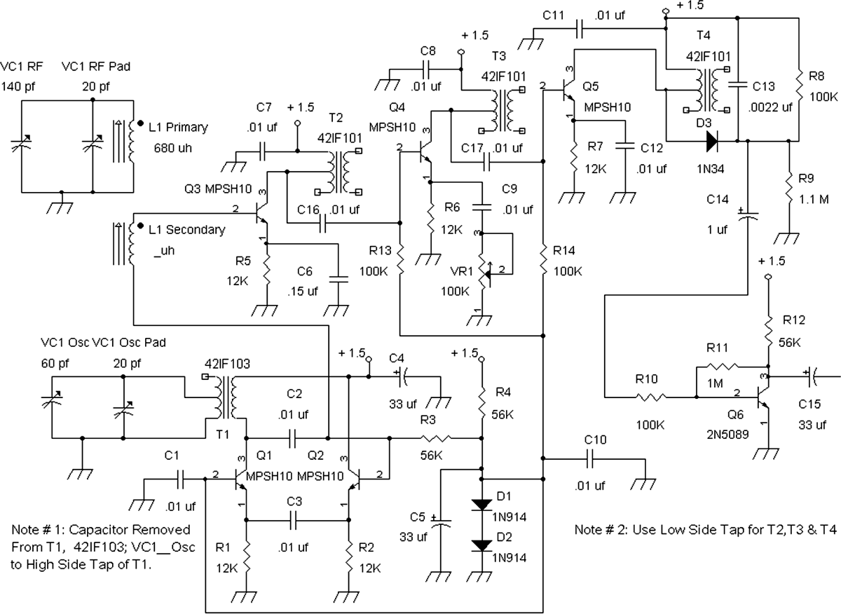
FIGURE 9-2 Schematic diagram of a six-transistor low-power superheterodyne radio.
For the oscillator circuit, a different approach is needed to achieve oscillations at low transistor collector currents. Also, because a conventional or off-the-shelf oscillator coil has too high a turns ratio, some other type of oscillator coil must be used for a low-power oscillator circuit.
Since the third IF transformer (the 42IF103) has a turns ratio of 6:1 instead of 20:1, it is possible to use it as an oscillator coil for a low-power circuit. The first step is to remove the internal capacitor by using a small-blade screwdriver to break out the ceramic material on the bottom of the 42IF103 IF transformer. The leads of the capacitor can stay and do not need to be removed. Alternatively, Xicon, which manufactures the IF transformer and oscillator coils, also makes a version of the 42IF103 without the capacitor, which is the 42IF106. The required inductance is about 330 μH, which is achieved across the high-side tap. Thus the variable capacitor VC1 is connected to the high-side tap connection of the primary of T1. This time the low-side tap connection of the 42IF103 or 42IF106 primary winding is left alone as an open circuit.
At resonance via VC1_Osc and the primary high-side tap winding of T1, the secondary winding has a sufficiently high load resistance for Q1 to set up a sustained oscillation via positive feedback via Q2. The oscillator’s output signal is about 170 mV peak to peak at C2. This oscillation signal is added to the radio-frequency (RF) signal from the secondary winding of L1. Many antenna coils come with a secondary winding. But some antenna coils come with just a primary winding. Thus a secondary winding can be made by winding about 10 to 20 turns of wire near or on the primary winding of the antenna coil.
It should be noted that the secondary winding can be made with more turns than usual because the input resistance to the mixer transistor Q3 is higher than usual owing to the lowered collector current. For example, most antenna coils come with a primary-to-secondary turns ratio of about 10 to 15:1. For this project, a turns ratio of 4 to 5:1 will provide more RF signal into the mixer transistor while still maintaining the high Q of the antenna coil.
With the RF signal added to the 170 mV of oscillator signal, mixer transistor Q3 is driven into gross distortion such that there is a multiplying effect of the RF signal and the oscillator signal. Thus the collector of Q3 includes a signal that is a frequency-translated (455-kHz) version of the RF signal.
IF transformer T2 works as an inductor capacitor tank circuit tuned to 455 kHz. The collector of Q3 is fed to the low-side tap of T2 so as to form a lower-impedance load. At the primary, the turns ratio from the whole winding to the low-side tap is about 3:1. The equivalent parallel resistance across the whole winding of the primary winding is about 500 k![]() . Thus the resistance at resonance at the low-side tap is 500 k
. Thus the resistance at resonance at the low-side tap is 500 k![]() divided by 3 × 3 = 9, or about 55 k
divided by 3 × 3 = 9, or about 55 k![]() .
.
By C16, the low-side tap of T2 is connected to the input of the first IF amplifier transistor Q4, which has an input resistance of greater than 100 k![]() .
.
![]()
The input resistance to a common or grounded emitter amplifier is the current gain divided by (DC collector current/0.026 volt). Assuming a current gain of 50 and a DC collector current of 12 μA, then the input resistance is about 50/0.000046mho = 108 k![]() .
.
IF amplifier Q4 also has a gain control, VR1, that provides a gain reduction of 8:1. When VR1 is adjusted for maximum gain (VR1 = 0 ![]() ), the input resistance of Q4 is about 108 k
), the input resistance of Q4 is about 108 k![]() . But when VR1 is set to 100 k
. But when VR1 is set to 100 k![]() , the gain of amplifier is lowered, but the input resistance is raised from 108 k
, the gain of amplifier is lowered, but the input resistance is raised from 108 k![]() to 108 k
to 108 k![]() 1 (50 1 1) × 10.7 k
1 (50 1 1) × 10.7 k![]() = 654 k
= 654 k![]() . The 10.7-k
. The 10.7-k![]() number is the parallel resistance of 100 k
number is the parallel resistance of 100 k![]() and 12 k
and 12 k![]() .
.
The output of Q4 via its collector is connected to the low-side tap of the primary winding of T3 and coupled to the second IF amplifier Q5 via C17. The second IF amplifier’s input resistance is similar to that of the Q4 amplifier and equals about 100 kV or more.
A germanium diode (D3) demodulates the 455-kHz AM signal at the collector of Q5. R8 and R9 provide about 100 mV of forward voltage bias to the germanium diode detector. Audio signals from the cathode of D3 are amplified further by Q6, an inverting audio amplifier, to drive the crystal earphone via C15.
Alternative Low-Power Superheterodyne Radio Design
Figure 9-3 presents a slight modification to the preceding design. By using a twin variable capacitor, the two-transistor oscillator circuit can use an IF transformer with its internal capacitor removed or, better yet, a standard variable inductor.

FIGURE 9-3 A low-power superheterodyne radio with a twin-gang variable capacitor.
Parts List
• Cl, C2, C3, C7, C8, C9, C10, C11 , C12, C17, C18, C19, C20: 0.01 μF
• C4, C5, C15: 33 μF, 16 volts
• C6: 0.15 μF
• C13: 0.0022 μF
• C14: 1 μF, 35 volts or 33 μF, 16 volts
• C16: 330 pF
• Rl, R2: 22 k![]()
• R5, R6, R7: 12 k![]()
• R8, RIO , R13, R14, R15: 100 k![]()
• R9: 1.1 M![]()
• R11 : 1 M![]() or 1.1 M
or 1.1 M![]()
• Dl, D2: 1N914
• D3: 1N34 or 1N270
• Ql, Q2, Q3, Q4, Q5: MPSH10
• Q6: 2N5089 or 2N5088
• LI antenna coil: 330 μH primary, 10 to 20 turns for secondary winding
• T1: 42IF101 IF transformer with internal capacitor removed, or a 120-μH or 150-μH variable inductor
• T2, T3, T4: 42IF101 IF transformer
• VC1 variable capacitor: twin gang 270 pF and 270 pF
• VR1: 100-k![]() pot
pot
Figure 9-4 presents a schematic diagram of the alternate low-power superheterodyne radio. In this configuration, the oscillator tank circuit formed by VC1, C16, and T1 is not stepped down via a secondary winding but rather is connected via C2 to the base of Q2. This means that at resonance, Q1’s collector load is a resistance of at least 10 k![]() . This higher load resistance at the collector of Q1 provides more overall gain in the circuit for oscillation. However, because the collector of Q1 is sensitive to stray capacitance that will shift the oscillation frequency, the output signal from the oscillator is taken from the emitter of Q2, a lower-resistance point. Any small stray capacitance loading into the emitter of Q2 does not cause the oscillator’s frequency to shift.
. This higher load resistance at the collector of Q1 provides more overall gain in the circuit for oscillation. However, because the collector of Q1 is sensitive to stray capacitance that will shift the oscillation frequency, the output signal from the oscillator is taken from the emitter of Q2, a lower-resistance point. Any small stray capacitance loading into the emitter of Q2 does not cause the oscillator’s frequency to shift.
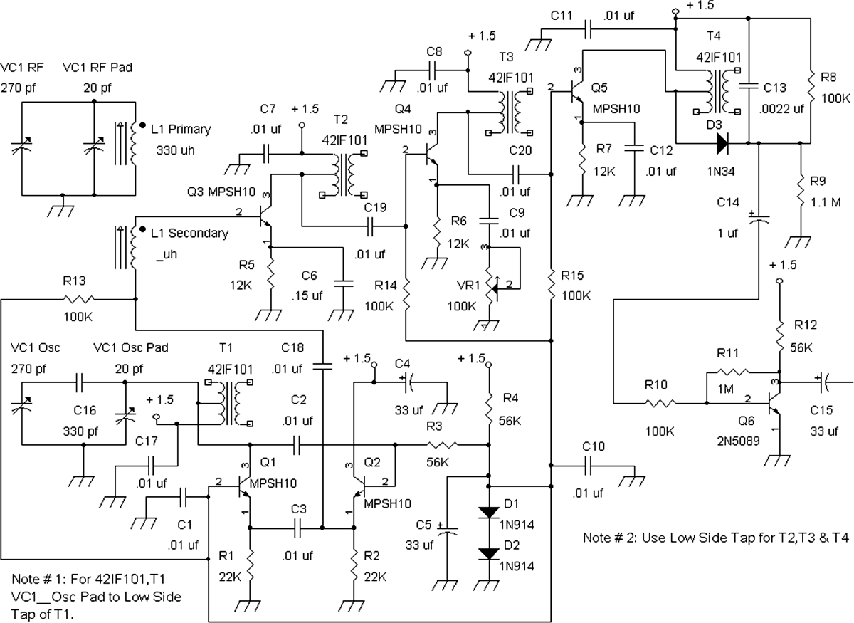
FIGURE 9-4 Schematic diagram for the alternate low-power superheterodyne radio.
The waveform at the Q2 emitter is a half-wave-rectified sine wave, which resembles a positive-going pulse. This positive-going pulse then is added to the RF signal from L1’s secondary winding and fed to the mixer Q3. From here on out, the circuit works identically to the one shown in Figure 9-2.
This radio drained about 97 μA at 1.25 volts, but the reader is encouraged to change the values of R1 and R2 from 22 k![]() to 33 k
to 33 k![]() (or 39 k
(or 39 k![]() ) and change R3 from 56 k
) and change R3 from 56 k![]() to 75 k
to 75 k![]() or 100 k
or 100 k![]() to lower the power consumption further.
to lower the power consumption further.
It should be noted that the reader also can replace the ferrite antenna coil L1 in Figure 9-4 with a loop antenna and an RF transformer (actually an oscillator coil used as an RF coil), such as the 42IF100, 42IF110, or 42IF300 coil. The loop antenna will be connected to the low-side tap of the RF transformer at the primary winding, the variable capacitor VC1’s RF section will be connected to the primary winding, and the other end of the primary winding will be grounded. The secondary winding of the RF transformer will be connected in the same way as the secondary winding of L1 in Figure 9-4. For a reference, see Figure 8-8 for the schematic pertaining to the loop antenna and T7.
Photos of Low-Power AM Superheterodyne Radios
Figure 9-5 is a picture of a prototype of the circuit from Figure 9-2. Figure 9-6 shows the original low-power AM superheterodyne radio that was featured in EDN Magazine. This radio lasted about five years on a C cell. It drained about 140 μA to 150 μA depending on the setting of the IF gain control (on the right side of the radio). This radio used a similar circuit to that shown in Figure 9-2. However, the oscillator coil was hacked or modified extensively to match the variable capacitor and to ensure that the low-power differential-pair transistor oscillator circuit performed as expected. For making this oscillator coil, an IF transformer was taken apart, and the primary winding was unwound and then rewound to achieve the correct inductance and tapping ratio. Excess wire was cut off because an oscillator coil generally has less inductance than an IF coil. Also, this procedure of unwinding and rewinding the coil was very challenging because the thickness of the wire in the IF transformer was about the same thickness as a human hair.
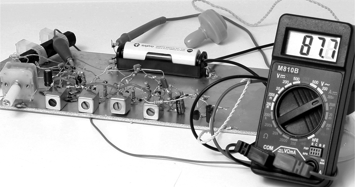
FIGURE 9-5 A superheterodyne radio that drains about 87 μA from an NiMH battery.
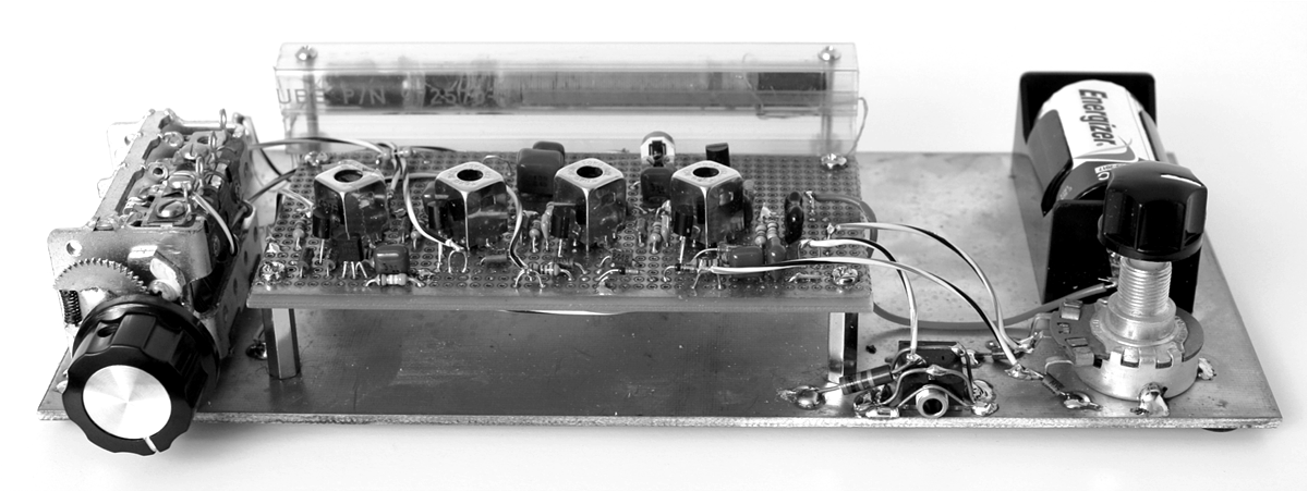
FIGURE 9-6 Original low-power superheterodyne radio.
See below for the schematic diagram of Figure 9-6.
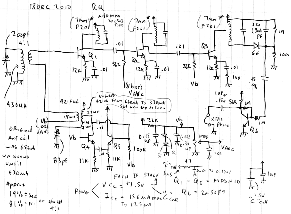
FIGURE 9-7 Schematic diagram of the original low-power superheterodyne radio.