Chapter 18
Detector/Automatic Volume Control Circuits
Although the title of this chapter may seem to cover simple circuits, the analysis of some detector circuits and automatic volume control (AVC) systems can be quite detailed and extremely tedious. In particular, a peak-envelope amplitude-modulation (AM) detector such as that shown in Figure 18-1 with D3, C13, R8, and R9 is actually very hard to analyze in terms of calculating for distortion, bandwidth, and reduction of Q of the tank circuit. Depending on the amount of modulation on the envelope, the resistor-capacitor discharge current varies.
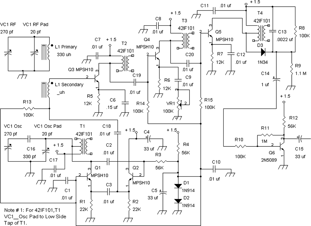
FIGURE 18-1 A superheterodyne radio with a peak envelope detector D3.
An approximation for a peak detector is to analyze it as a sample-and-hold circuit. Each peak cycle of the carrier is rectified to a positive pulse that charges a capacitor that acts as if each peak were sampled and held. But still the analysis of the peak envelope detectors is tricky and really long.
Here is a quote from Harold S. Black from his 1953 book, Modulation Theory, regarding peak envelope detectors: “Detailed analysis of the current wave that flows, or the spectrum of the voltage across the load resistance, tends to get tedious and not to produce results in an interesting form.”
Therefore, this chapter will take a look at average envelope detection for AM signals, which does not include a charging capacitor such as C13 in Figure 18-1. However, for an excellent and detailed analysis of AM detectors and in particular peak envelope detectors, please read Chapter 10 of Communications Circuits Analysis and Design, by Clarke and Hess.
In terms of AVC circuits, the analysis of this feedback system is also very involved. Unlike many standard feedback systems, where a reference signal forces the output to a predetermined amplitude level, AVC systems are unique in that there is no reference signal. The output of an amplifier is converted to a direct-current (DC) signal and fed back to a gain-control terminal of the radio-frequency (RF), intermediate-frequency (IF), and or mixer circuits.
Therefore, this chapter will investigate certain aspects of AM detectors. The objectives are
1. To examine averaging envelope detectors and power detectors.
2. To look into synchronous detector circuits for single- and double-sideband signals.
3. To explain how AM radio I and Q signals are demodulated without envelope or synchronous detection.
4. To measure the average carrier signal for an AVC system.
Average Envelope Detectors
Figure 18-2 shows an envelope detector consisting of a diode D1 and resistor R1. For analysis of this circuit, the diode is “perfect” in that there is no turn voltage such as 0.1 volt for germanium or 0.5 volt for silicon diodes. Figure 18-3 shows a biasing scheme consisting of resistor R2 and diode D2 to overcome the turn on voltage of germanium or silicon diodes. (Note: R2D2 can be bought at your local electronics parts vendor, so you do not have to travel to a galaxy far, far away to get them—just kidding!) Diodes D1 and D2 are of the same semiconductor material.
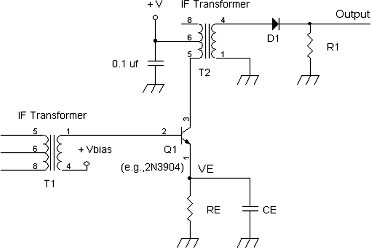
Note: Each IF Transformer has an internal capacitor.
FIGURE 18-2 A typical average envelope detector for standard AM signals.
Note: Each IF Transformer has an internal capacitor.
FIGURE 18-3 A biasing circuit to overcome the turn on voltage of a diode or transistor.
For analyzing a rectifying demodulator for a standard AM signal such as the one shown in Figure 18-4, we assume the following:
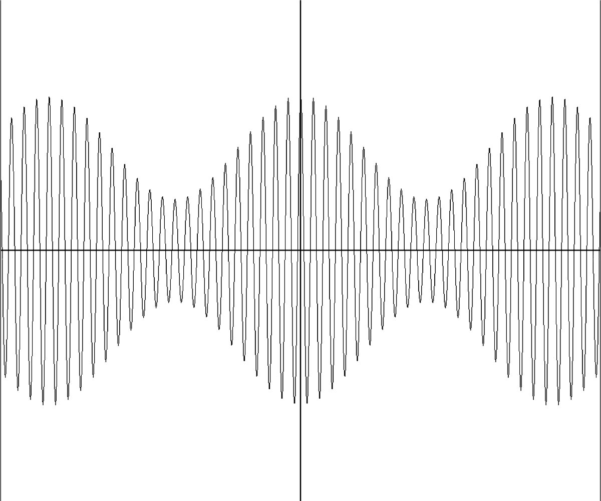
FIGURE 18-4 An AM signal that is fed into the diode detector circuit.
1. The diode has no voltage drop.
2. The diode detector is driven by a sufficiently low resistance that the load resistor R does not load down the IF signal.
![]()
The waveforms shown, unless noted, have the X axis for time and the Y axis for amplitude.
Figure 18-4 is characterized by equation
![]()
If the modulating signal m(t) = 0, then all we have is the carrier and an unmodulated AM signal.
For an unmodulated signal, the output of the diode rectifier provided a half-wave-rectified signal. This rectified signal should not be confused with any exponential characteristic of the typical semiconductor diode such as
![]()
In fact, the diode is basically switching or gating only one polarity of the AM signal into the load resistor. Therefore, any power-series analysis of the exponential function is not applicable because switching or gating effects result in discontinuities in the half-wave-rectified waveform that are not associated with the exponential function.
The output of the rectifier for an unmodulated AM signal is seen in Figure 18-5. The half-wave-rectified signal (HWRS) of peak amplitude Vp, as seen in Figure 18-5, can be described by the following Fourier series:
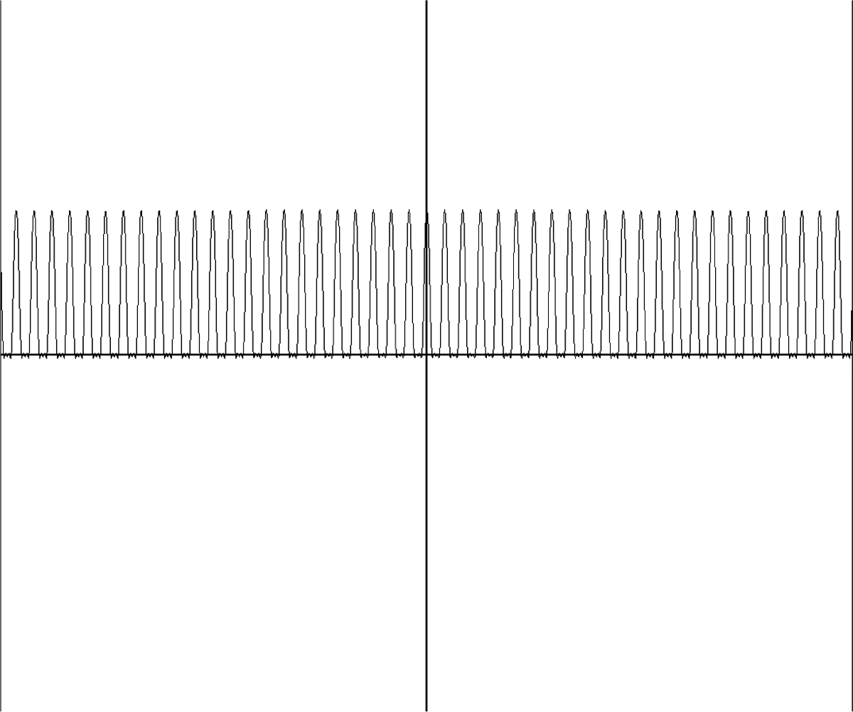
FIGURE 18-5 Output signal of the diode rectifier of an unmodulated AM signal.
![]()
Figure 18-6 shows a rectified modulated signal. The figure shows an AM signal that is being demodulated by half-wave rectification. To relate to this waveform, it is equivalent to multiplying the half-wave unmodulated waveform from Figure 18-5 with the same modulating signal [1 + m(t)].

FIGURE 18-6 A modulated AM signal is half-wave rectified via a diode circuit.
Therefore, the formula that describes a demodulated AM signal for average envelope detection is
![]()
To recover the modulated signal and its average carrier level, the high-frequency signals related to the frequency fIF and harmonics of fIF are removed by filtering. As a result of filtering, the output of the demodulator is
![]()
Therefore, the output of the demodulator for an average envelope detector is
![]()
which means that the audio output signal is scaled by (1/π) = 0.318. So as compared with a peak detector, the average envelope detector provides only about 32 percent of the audio level of a peak detector. For example, if m(t) 5 (½) cos(2pfmod)t, the output of the demodulator is
![]()
Figure 18-7 shows the half-wave-rectified AM signal with the filtered modulating signal. Had a full-wave rectifier been used instead of the half-wave circuit, the output of the average envelope detector would be twice the audio level, or a scaling factor of (2/π), which then would approach the demodulated output of a peak envelope detector.
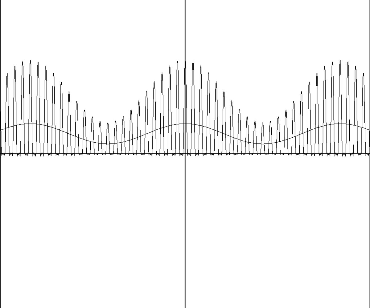
FIGURE 18-7 Demodulated AM signal with audio signal at (1/π) of the carrier level.
However, full rectification of the IF signal for detection is rarely used because matched diodes and a center-tapped secondary winding of the IF transformer are needed, which adds to the cost. Most AM demodulators just use a peak envelope detector.
Power Detectors
Power detectors for AM broadcast signals have been around since the days of vacuum-tube regenerative radios. The basic premise of a power detector is to take advantage of the “inherent” nonlinearity in active devices such as tubes, field-effect transistors (FETs), or transistors. Power detectors also have an advantage over diode demodulators. They provide a higher load resistance to the IF tank circuit, which maintains a higher Q or selectivity in the last IF stage.
In Chapter 17 we looked at the consequences of second- and third-order distortions of IF signals. For a square-law device, the output current for an AM signal is
![]()
Note that the input signal into the square-law device is
![]()
Vsig is represented in Figure 18-4. Also note that since second-order distortion rises as the square of the input signal, increasing this input signal results in more distortion and more output in terms of the demodulated signal. However, for small amplitudes of the input signal [1 + m(t)] cos(2πfIF)t, there should be less “conversion gain” for audio signals.
In particular, the second-order distortion produced signals such as baseband audio signals and second harmonic IF signals that can be filtered out by the IF transformer.
We now turn our attention to the baseband signal. In the second-ordered term, there is a squared cosine term [cos(2πfIF)t]2 = (½)[1 + [cos(2π2fIF)t]. When a low-pass filter is applied, the high-frequency signal cos(2π2fIF)t is removed, leaving only the (½)(1) = (½) term [see Equation (18-5)].
For a device that generates second-order harmonic distortion with the high-frequency IF signal and its harmonics filtered out, the output current is given by
![]()
As can be seen, after filtering, the modulating signal m(t) is recovered. However, there is a distortion term m(t)2 that adds second-harmonic distortion to the recovered audio signal. At first glance, the second-harmonic distortion terms looks really bad because given 100 percent modulation for a sine-wave-modulating signal, the second-harmonic distortion can be 25 percent of the amplitude of the recovered audio signal. For example, if m(t) 5 cos(2pfmod)t for 100 percent modulation, then
However, the relative level of the recovered audio signal is 2m(t) 5 cos(2pfmodt), which leads to the fact that there is a 4:1 ratio between the recovered audio signal and its second harmonic.
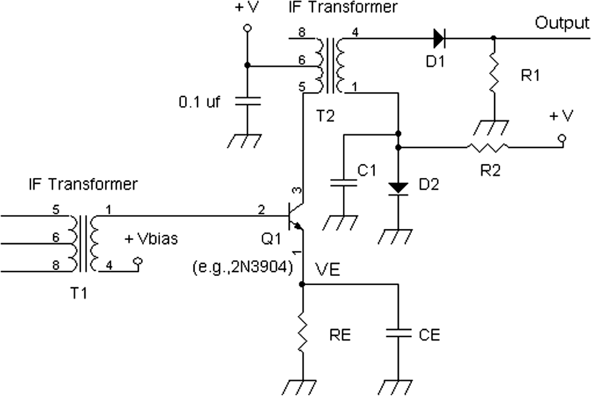
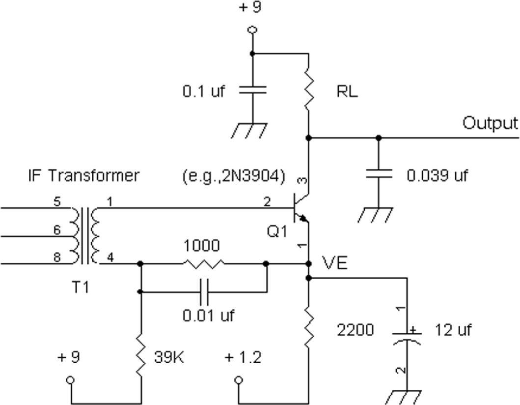
However, when one listens subjectively to a complex waveform such as speech or music, the power detector provides very tolerable and intelligible audio reproduction. Figures 18-8 and 18-9 show typical bipolar transistor power detector circuits. The power detector shown in Figure 18-8 is basically a common-emitter amplifier that has its emitter alternating-current (AC) grounded via the 12-μF capacitor. Grounding the emitter via capacitor CE is essential to take advantage of the inherent nonlinearity of the transistor. Figure 18-9 shows a slightly simplified version of the power detector circuit in Figure 18-8. Figure 18-10 shows the output current to a bipolar transistor power detector with 50 percent modulation.
Note: IF Transformer has an internal capacitor.
FIGURE 18-8 A power detector circuit from the Motorola 56T transistor radio from 1956.
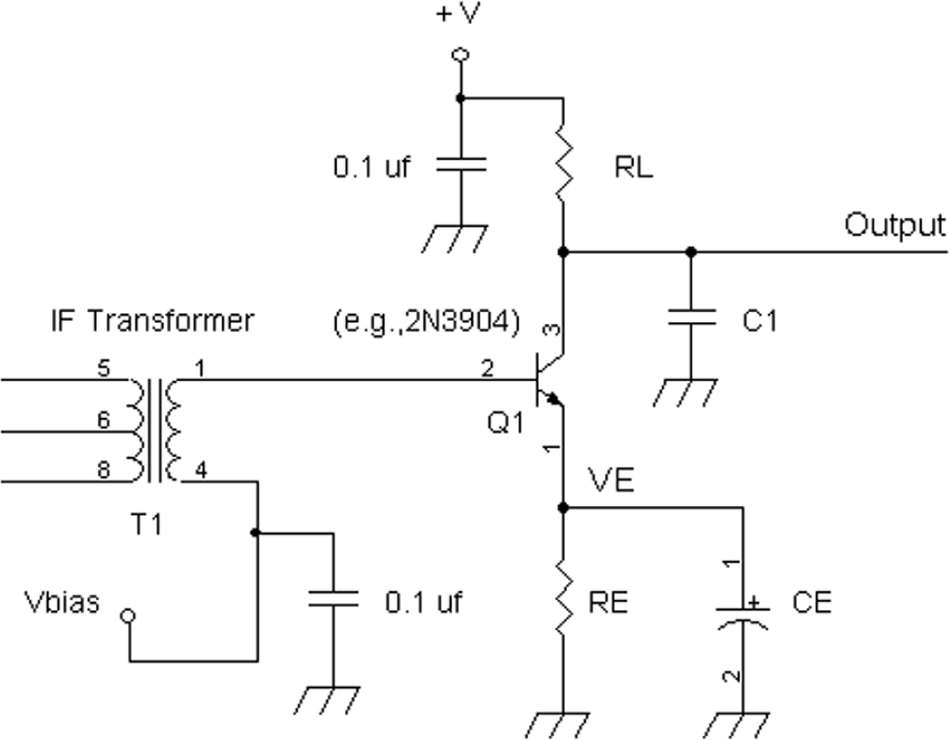
Note: IF Transformer has an internal capacitor.
FIGURE 18-9 A more simplified power detector circuit.
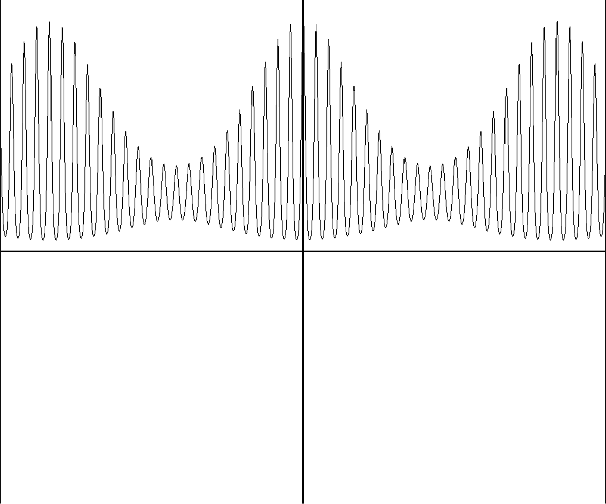
FIGURE 18-10 Collector current with an AM signal at the base.
Although bipolar transistors have third-, fourth-, and higher-harmonic distortion, in practice, when they are used as a power detector, the bipolar transistor’s exponential curve approximates square-law power detection very closely. That is, when the audio signal is measured at the output of the collector of Figures 18-8 or 18-9, the third harmonic is typically 10 times lower than the second harmonic.
Measurements were done on the circuit in Figure 18-9 and produced the following parameters:
• C1 5 0.022 μF
• CE 5 4.7 μF (Note: The capacitance of CE can be larger, such as 10 μF to 33 μF.)
• RE 5 RL 5 1,000 ![]()
• VE 5 0.72 V
• ICQ = 0.72 mA
• gm = 0.0277 mho or S
• fmod = 500 Hz
• fIF = 455 kHz
• 50 percent modulation was used.
• V sig = 100 mV {[1 + 0.5 cos(2πfmod)t] cos(2πIF )t}
• Power detector output = 380 mV[0.5 cos(2πfmod)t]
• The second-harmonic distortion was about 7 percent, whereas the third-harmonic distortion was about 0.7 percent.
• A lower-level IF signal was coupled into the power detector.
• Vsig = 40 mV [1 + 0.5 cos(2πfmod )t] cos(2πfIF) t
• Power detector output = 110 mV [0.5 cos(2πfmod)t]
• The second-harmonic distortion was about 12 percent, whereas the third-harmonic distortion was about 1.2 percent.
Note that when the input signal dropped from 100 mV to 40 mV, a factor of 2.5:1, the detector ouput dropped from 380 mV to 110 mV, a factor of 3.45:1. This shows that reducing the IF signal level also reduces the “conversion gain” on recovering the audio signal. Of course, this makes sense because when the IF signal is very small, the common-emitter amplifier does not create the distortion needed for AM detection and thus provides very little or no demodulated signals.
One may notice that the power detector provides demodulated audio signal and amplification of the demodulated signal. For the input signal
![]()
the power detector provided a demodulated output signal of 380 mV peak. In contrast, a peak envelope detector will provide only 50 mV peak (100 mV × 0.5).
And more gain from the power detector can be provided by any combination of increasing the DC collector current or the collector load resistor. For example, increasing the load resistor from 1,000 V to 2,000 V will double the amplitude of the demodulated signal to provide 760 mV in peak amplitude of the audio signal.
In practical terms, a superheterodyne receiver that uses a power detector must provide adequate IF signal levels to the detector to deliberately drive the transistor into distortion. Thus better performance will be achieved by radios with two IF stages than just a single IF amplifier.
Synchronous Detectors
Synchronous detectors are often used in three situations. One is for the detection of Morse code transmission. Another is for the demodulation of suppressed carrier signals such as single- or double-sideband signals. In Chapter 17, synchronous detection of double- and single-sideband AM signals was discussed. The third common use for a synchronous detector is to provide much better demodulation fidelity of standard AM signals. When envelope detectors are used, generally fairly good distortion performance can be achieved. However, synchronous detectors can be used to further lower distortion when demodulating an AM signal. For analog-transmitted television signals, amplitude modulation is used. And in the television receiver, generally a diode envelope detector is used. However, with integrated circuits (ICs), including many complex circuits as part of a television signal system, synchronous detectors are used instead of envelope detectors.
At the IC level, adding more transistors and resistors is not much of a problem, and the cost is negligible. But on a printed-circuit-board implementation, adding extra functions with more parts takes up board space and adds cost. Therefore, when more circuits were literally integrated into the chips, complex demodulation systems were designed routinely.
The basic synchronous detector requires two circuits at a minimum. One circuit is the carrier regeneration circuit that provides a continuous-wave (CW) signal that represents the carrier signal, and the other circuit is a multiplier to provide the demodulation.
Figure 18-11 shows a typical synchronous detector used for demodulating AM signals. A phase-lock loop circuit consisting of the phase detector, loop filter amplifier, and voltage-controlled oscillator (VCO) regenerates the IF carrier signal. Demodulation of a standard AM signal is achieved by multiplying a phase-shifted version of the VCO output with the IF signal.

FIGURE 18-11 A synchronous detector with a phase-lock loop oscillator and mixer for detecting AM signals.
The AM IF signal is fed to an amplifier and a band-pass filter for increasing the level of the IF signal and filtering out some of the noise that may be present. With a sufficient level of the IF signal, a limiter further amplifies and detects the zero crossings of the IF signal. These zero crossings provide the phase information needed for regeneration of the carrier signal. In this particular example, the output of the limiter circuit provides a square-wave signal, which then is connected to an input of a phase comparator. The output of the phase comparator, such as an Exclusive OR gate, will provide an average voltage based on the phase difference between the IF signal and the VCO. Normally, if an Exclusive OR gate is used, the phase that is desired for the VCO to lock is 90 degrees away from the incoming IF signal, which then outputs an average voltage from the Exclusive OR gate of one-half the supply voltage. For example, if the supply voltage is 5 volts, when the VCO is typically locked, the average output voltage from the Exclusive OR phase detector is 2.5 volts DC.
The output of the phase detector then is coupled to an amplifier and low-pass filter (loop filter amplifier), which then feeds an error-correction signal into the VCO. The phase-lock loop circuit provides a CW signal. This CW signal then has the average phase of the IF signal carrier. However, care must be taken such that the VCO itself does not generate too much phase noise. Thus, normally, the VCO consists of a high-stability oscillator such as an LC oscillator. The VCO provides a signal whose frequency depends on the voltage into the VCO. The output of the VCO then is coupled to the remaining input of the phase detector.
Therefore, the output of the VCO provides a regenerated carrier signal of constant amplitude. Because the phase detector locks the VCO to the IF signal’s carrier with a 90-degree offset, a phase-shifter circuit is provided to cancel the 90-degree offset and match the IF signal carrier’s phase. Thus the output of the phase-shifter circuit is connected to one input of a multiplying circuit, and the other input of the multiplier circuit is connected to the IF signal. The output of the multiplier then is low-pass-filtered to recover the audio signal.
Of course, there are many variations on how carrier regeneration can be done. Figure 18-11 is just one example. For readers who are interested in a “jungle chip” that demodulates AM TV signals, the Mitsubishi M51366SP integrated circuit is an example.
IQ Detectors for AM Broadcast Signals
For software-defined radios (SDRs), demodulating a standard AM signal, a double-sideband signal with carrier, is implemented entirely differently. There is no envelope detector, and although synchronous detection can be used, detection of the standard AM signal is done via a Pythagorean process. That is, a key to understanding this type of demodulation process will include the trigonometric identity [cos(θ)]2 1 [sin(θ)]2 = 1 (Figure 18-12).

FIGURE 18-12 Demodulating AM signals via a Pythagorean method.
Figure 18-12 shows two signals—the I Signal Vsig_I and the Q Signal Vsig_Q—that are individually squared and added. For simplicity, the analysis will be done in the continuous time domain. The analog-to-digital converters (ADC_I and ADC_Q) and digital-to-analog converter (DAC) can be omitted for the analysis below. The square root of the output of the adder then provides the demodulated signal, such as an audio signal. For a general situation, the two signals are defined as follows:
![]()
The output of squaring function SQ_1 is
![]()
and the output of squaring function SQ_2 is
![]()
And the output of the adder is

However, we know that [cos(θ)]2 + [sin(θ)]2 = 1, and we let θ = (2πfIF)t. Therefore, [cos(2πfIF)t]2 + [sin(2πfIF)t]2 = 1, and the summed or added output is
![]()
The output of the adder is connected to the input of a square-root function, so the positive output of the square-root function is
![]()
and the output of the square-root function provides a DC offset signal (1) that represents the carrier level at 0 modulation.
Figure 18-12 also includes the analog-to-digital converters and a digital-to-analog converter to denote that normally the I and Q signals are digitized, and the squaring, summing, and square-root functions are implemented in a computational manner.
At this point in this chapter, it would seem that the explanation on how I and Q signals are demodulated for AM signals is done. Well, not so fast. There is one equation that may need further explanation. In high school trigonometry classes, the trigonometric identity [cos(θ)]2 + [sin(θ)]2 5 + is “taken for granted.” After all, the angle addition and subtraction laws prove this identity. But what does it really represent in terms of time-varying signals? The idea of taking the sum of the squares of the cosine and sine functions of the same angle and having this sum equal to 1 seems a bit abstract. Let’s see what is really going on by graphing out the cosine and sine functions.
Figure 18-13 presents graphs of cos(2πfIF)t and [cos(2πfIF)t]2. The squared cosine signal has a twice-frequency signal that is half the amplitude of the cosine signal, and the squared cosine signal includes a DC signal at one-half the peak amplitude of the cosine signal. Since the peak amplitude of the cosine signal is 1, the DC signal has a value of 0.5.

FIGURE 18-13 Graphs of a cosine signal and a squared cosine signal.
Figure 18-14 shows graphs of a sine signal and the square of the sine signal. Because the sine signal is one-quarter of a cycle or 90 degrees shifted from the cosine signal, the squared sine signal will produce a twice-frequency signal that is one-half cycle or 180 degrees in relationship to the twice-frequency cosine signal.

FIGURE 18-14 Graphs of a sine signal and a squared sine signal.
Very much like the squared cosine signal, the squared sine signal has twice the frequency and half the amplitude of the sine signal. Also, the squared signal has a DC signal of 0.5.
Now let’s take a look at two squared signals. Figure 18-15 displays the two squared signals. When the squared cosine signal and the squared sine signal are added or summed, the twice-frequency signals are 180 degrees from each other and will cancel, whereas the DC signals that are each 0.5 in amplitude will add to form a DC signal of 1.0. Thus the sum of the squares of the cosine and sine signals of the same frequency is a constant 1 (Figure 18-16).
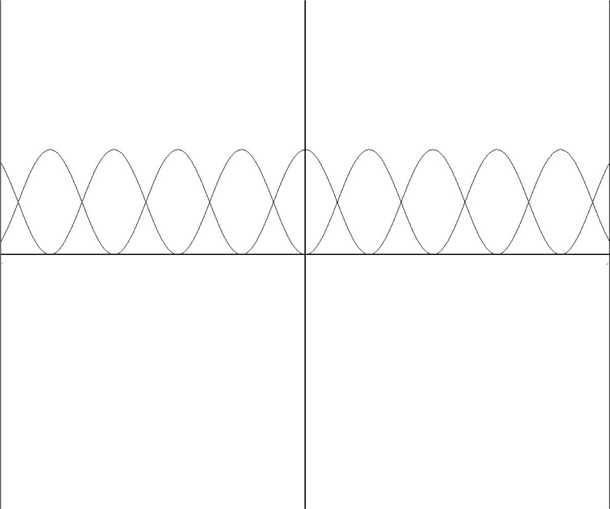
FIGURE 18-15 The squared cosine signal and the squared sine signal shown together.
As seen in Figure 18-16, the sum of the two twice-frequency signals with 0.5 DC offsets result in a DC value of 1.0. Thus, in terms of time functions, the sum of the squares of 0-degree cosine and 90-degree sine signals produces a frequency-doubling effect that results in twice the phase shift of 180 degrees. The twice-frequency AC signals cancel out to zero, whereas the DC components of 0.5 add to form 1, which is the result for [cos(θ)]2 + [sin(θ)]2 = 1 for any θ.

FIGURE 18-16 The sum of the waveforms shown in Figure 18-15.
Measuring an Average Carrier or Providing Automatic Volume Control
In designing an AVC system for an AM radio, there is one very important factor to consider, and that is defining the maximum carrier level from the output of the IF transformer. By defining the maximum carrier level, the maximum audio level also is defined. For example an average carrier level of 1.0 volt peak provides 1.0 volt peak of audio at 100 percent modulation (Figure 18-17). From Equation (16-1) in Chapter 16, {1 + m[cos(2πfmod)t]} cos(2πfcarrier)t = AM signal.
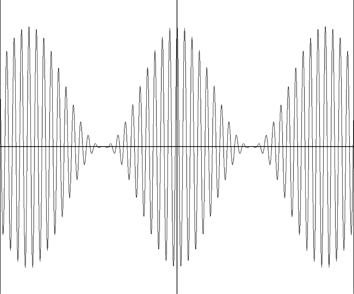
FIGURE 18-17 An AM signal with 1.0-V peak average carrier level with an audio signal of 1.0 volt.
An AVC system is shown in Figure 18-18. The figure shows an IF system and detector of a superheterodyne radio with the level-shifter resistor and capacitor values for R2, C3, R3, and R4 similar to those in the Sony Model 3F-66W radio.
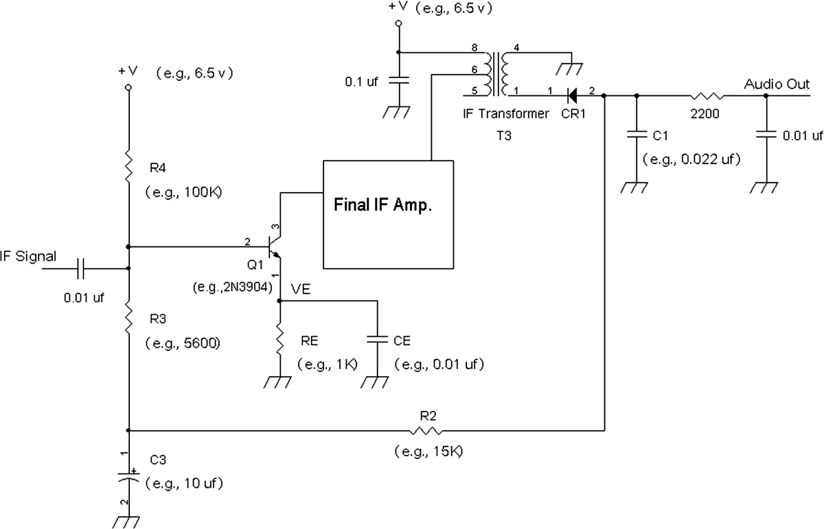
Note: IF Transformer has an internal capacitor.
FIGURE 18-18 An AVC system using a negative peak detector and DC level shifter.
The AM signal is demodulated by a negative peak detector CR1 and C1 that follows the audio signal. The output of the negative peak detector at the anode of CR1 provides the negative going peaks of the AM signal that is level-shifted by about +0.6 volt owing to the turn-on voltage of diode CR1. When the AM signal is very weak or near zero, the output of CR1 is about +0.6 volt. When the AM signal is strong, the output of CR1 is less than +0.6 volt because of the negative peak detector CR1 and hold capacitor C1.
Resistor R2 and capacitor C3 remove the audio signal and provide a DC voltage that is indicative of the negative peak voltage of an unmodulated AM signal.
To design the AVC system as shown in Figure 18-18 for a particular audio level Vpk_audio, and given a silicon diode and transistor with about a 0.6-volt forward voltage drop, then all that is needed is a level-shifting circuit that provides Vpeak_audio of DC bias to the emitter voltage VE. For example, if 400 mV peak audio is required, then 0.4 volt DC is needed for VE under a weak- or no-signal condition. The level-shifting circuit, consisting of CR1, R2, R3, and R4, along with the power supply, then will provide a Q1 base voltage of about 0.6 volt + 0.4 volt 5 1.0 volt.
In Figure 18-18, assume that the diode and transistor turn-on voltages are the same. And thus the level-shifting voltage at a no-signal condition is the same voltage as the emitter voltage VE. If at 100 percent modulation, 500 mV peak audio is needed, and the voltage drop across R3 and R2 is about 500 mV DC given that R4 >> R3 + R2. Normally, the resistance of R4 is at least four times the series resistance of R2 and R3. When a weak station is received, the average DC voltage at C1 is about 0.6 volt. With the 0.5-volt level-shifting voltage from R2 and R3, the base voltage is about 1.1 volts for an emitter voltage of about 0.5 volt to set up a DC collector current of (+0.5 volt)/RE = ICQ1 However, when a very strong station is received, the negative peak value of the IF signal will be negative 0.5 volt. This negative 0.5 volt then is added to the +0.6-volt DC level-shifting voltage of CR1, resulting in a net average voltage of +0.1 volt DC at C1. With the + 0.5-volt level-shifting voltage across R2 and R3, the base of Q1 then has a voltage of +0.6 volt. However, the base-to-emitter voltage of Q1 is about +0.6 volt, which results in the emitter voltage approaching 0 volt across RE that results in nearly 0 collector current to reduce the gain of Q1. Figure 18-18 also includes in parenthesis values taken from a schematic of the Sony 3F-66W transistor radio from 1969. In this radio, Q1 is a silicon transistor, but the detector diode CR1 is germanium with a turn-on voltage of about 100 mV. With about 6.5 V powering R4, there is about 53 μA of current through the resistors R4, R3, and R2. The total resistance of R2 and R3 is 15 k![]() + 5.6 k
+ 5.6 k![]() = 20.6 k
= 20.6 k![]() . The voltage drop across R2 and R3 under no-signal conditions is 53 μA × 20.6 k
. The voltage drop across R2 and R3 under no-signal conditions is 53 μA × 20.6 k![]() = 1.09 volts and is also the level-shifting voltage that will be added to the CR1 diode drop of 0.1 volt. Thus the total voltage at the base of Q1 is 1.09 volt + 0.1 volt = 1.19 volt. The voltage at VE given a +0.6-volt base-emitter voltage drop for Q1 then is 1.19 volts - 0.6 volt = + 0.59 volt = VE. Thus the maximum expected audio amplitude is about 0.59 volt peak {§} when a strong station is tuned.
= 1.09 volts and is also the level-shifting voltage that will be added to the CR1 diode drop of 0.1 volt. Thus the total voltage at the base of Q1 is 1.09 volt + 0.1 volt = 1.19 volt. The voltage at VE given a +0.6-volt base-emitter voltage drop for Q1 then is 1.19 volts - 0.6 volt = + 0.59 volt = VE. Thus the maximum expected audio amplitude is about 0.59 volt peak {§} when a strong station is tuned.
References
1. Class Notes EE140, Robert G. Meyer, UC Berkeley, Fall 1975.
2. Class Notes EE240, Robert G. Meyer, UC Berkeley, Spring 1976.
3. Paul R. Gray and Robert G. Meyer, Analysis and Design of Analog Integrated Circuits, 3rd ed. New York, John Wiley & Sons, 1993.
4. Kenneth K. Clarke and Donald T. Hess, Communication Circuits: Analysis and Design. Reading: Addison-Wesley, 1971.
5. Robert L. Shrader, Electronic Communication, 6th ed. New York: Glencoe/McGraw-Hill, 1991.
6. Howard W. Sams & Co., Sams Photofact Transistor Radio Series, TSM-2. Indianapolis: November 1958.
7. Howard W. Sams & Co., Sams Photofact Transistor Radio Series, TSM-100. Indianapolis: May 1969.
8. Mary P. Dolciani, Simon L. Bergman, and William Wooton, Modern Algebra and Trigonometry. New York: Houghton Mifflin 1963.
9. William E. Boyce and Richard C. DiPrima, Elementary Differential Equations and Boundary Valued Problems. New York: John Wiley & Sons, 1977.