Chapter 22
Noise
This chapter covers the basic concepts behind random noise (e.g., hiss). In radio circuits, the noise in a front-end circuit hampers the ability to pick out weak radio-frequency (RF) signals. In audio circuits, the noise sources degrade the signal-to-noise ratio in mostly preamp circuits such as microphone preamplifiers. However, as mentioned in Chapter 12, where op amps and mixers are used in software-defined radio (SDR) front-end circuits, the noise contribution not only from the mixer circuits but also from the intermediate-frequency (IF) amplifiers can hamper reception of weak signals. In this chapter, the examination of noise will be limited to amplifier circuits and not mixers.
Therefore, the objectives for this chapter are
1. To identify sources of electronic random noise
2. To present some basic noise theory or noise models, including analyzing noise in a single-transistor amplifier (including referred input noise), lowering noise via paralleling transistors, and analyzing noise in a differential-pair amplifier
3. To select op amps for noise performance
For more details on noise, several books are recommended:
1. National Semiconductor, Audio/Radio Handbook. Santa Clara: National Semiconductor Corporation, 1980.
2. Paul R. Gray and Robert G. Meyer, Analysis and Design of Analog Integrated Circuits, 3rd ed. New York: John Wiley & Sons, 1993.
3. R. E. Zeimer and W. H. Tranter, Principles of Communications. Boston: Houghton Mifflin Company, 1976.
In the Audio/Radio Handbook, the subject of noise is excellently written about in the section on preamplifiers. Analysis and Design of Analog Integrated Circuits, by Gray and Meyer, superbly covers the subject of noise in integrated circuits, which is also applicable to discrete devices. Actually, this book is a standard textbook on analog integrated circuits in many university classes. And in Principles of Communications, Appendix A, “Physical Noise Sources and Noise Calculations in Communication Systems,” a very good discussion of noise is provided.
Sources of Random Electronic Noise and Some Basic Noise Theory
Random electronic noise is not like periodic noise sources, such as power-supply noise, hum, or interfering noise from external signal generators. Instead, there are two main sources of random electronic noise: thermal noise and shot noise.
Thermal noise is present in all resistors no matter what type. That is, metal-film, carbon-film, carbon-composition, wire-wound, and oxide resistors all have thermal noise. Also, field-effect transistors (FETs) also generate thermal noise. Shot noise arises from current flow in diodes and bipolar-junction transistors. Older devices such as vacuum tubes also generate shot noise.
![]()
Random noise signals do not add or subtract the same way as the familiar voltage sources we use. When independent random noise signals are added in terms of current or voltage, the total noise voltage is the sum of the squares of the random noise voltages followed by taking the square root. For example, three independent noise voltages Vn1, Vn2, and Vn3 are added in the following manner:
![]()
Similarly, independent random noise current sources In1, In2, and In3 add in the same manner:
![]()
It should be noted that for most practical purposes, inductors and capacitors do not generate random noise. Figures 22-1A, 22-1B, and 22-1C show sources of thermal and shot noise.
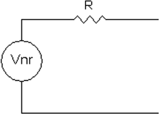
FIGURE 22-1A A noise model for resistors generating thermal noise.
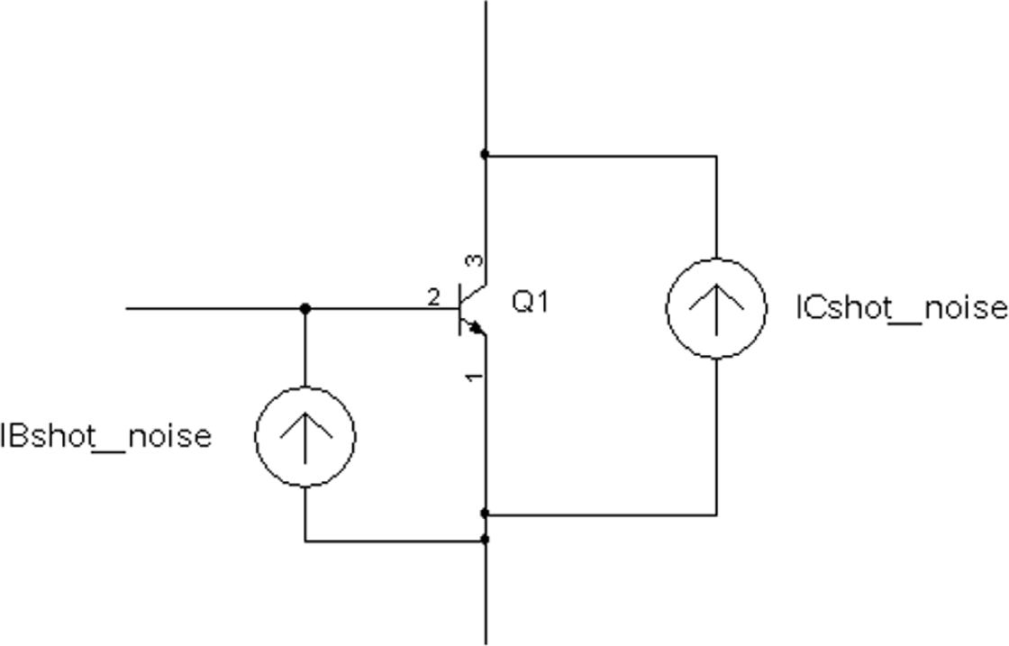
FIGURE 22-1B A noise model for shot-noise generators in a transistor
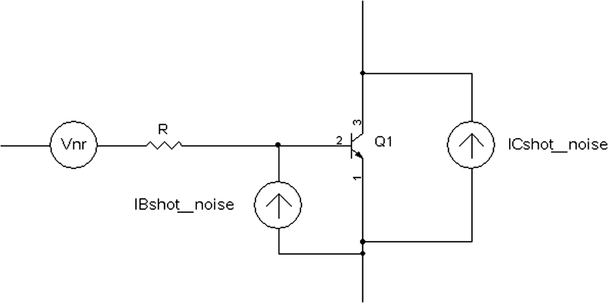
FIGURE 22-1C Thermal-and shot-noise components in a transistor
Before the actual noise of the resistors and shot-noise generators is calculated, we need a rough estimate of actual signal-to-noise ratio (SNR) for different types of products. SNR is the ratio of the signal in root-mean-square (RMS) voltage over the RMS noise voltage. In terms of sinusoidal signals, the RMS voltage is 0.707 × peak voltage = 0.707Vp. For example, a test sine-wave signal is given as Vp sin(2πft). Table 22-1 lists various devices and their SNRs.
Table 22-1 Signal-to-Noise Ratios of Various Devices
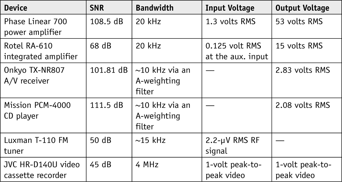
This table shows the SNRs of electronic devices ranging from audio amplifiers to a video recorder. What is important to note is that the SNR is usually measured at some input or output level for the sine-wave signal, and even more important, the noise is measured over a specific bandwidth. That is, the noise is usually measured from the device through a band-pass or low-pass filter of specified bandwidth.
Note that all the measurements in Table 22-1 refer to voltages, so
![]()
or, equivalently,
![]()
Therefore, when a device is measured and a noise measurement is given in an RMS voltage, one of the most important things to find out is: What is the bandwidth that the noise measurement is made under?
Let’s start off with the noise voltage caused by a resistor ![]() which is measured in RMS voltage, and where k is Bolzmann’s constant (= 1.38 × 10⁻²³), T is temperature in degrees kelvin (= 298 degrees K at room temperature), B is bandwidth in hertz, and R is resistance in ohms. That is,
which is measured in RMS voltage, and where k is Bolzmann’s constant (= 1.38 × 10⁻²³), T is temperature in degrees kelvin (= 298 degrees K at room temperature), B is bandwidth in hertz, and R is resistance in ohms. That is,
![]()
Thus, for a 1,000-![]() resistor with a bandwidth of 1 Hz,
resistor with a bandwidth of 1 Hz,
If the bandwidth is an audio bandwidth such as 10 kHz,
![]()
A normalized noise voltage expression is to set the bandwidth B to 1 Hz to provide a noise density voltage of
![]()
where Vx is noise voltage when bandwidth B = 1 Hz. For the 1,000-![]() resistor, Vx × 4.06 nV.
resistor, Vx × 4.06 nV.
To find the noise voltage, simply multiply the noise density voltage by the square root of the bandwidth. Noise voltage then can be expressed as
![]()
Therefore, from the preceding example for a 1,000-![]() resistor, the noise voltage is
resistor, the noise voltage is
![]()
And for B = 100 Hz, ![]()
For B = 20,000 ![]()
Also, it should be noted bandwidth B is defined by the difference of an upper frequency and a lower frequency. For example, for a bandwidth B of 20,000 Hz, the 1,000-V resistor produces 573 nV. Thus, if the noise is measured from 20,000 and 40,000 Hz or from 3,000 Hz to 23,000 Hz, then the noise voltage from a 1,000-![]() resistor is still 573 nV.
resistor is still 573 nV.
In one of the example devices listed in Table 22-1, the Phase Linear 700 amplifier had an SNR of 108.5 dB for 1.3 volts at an input. Figure 22-2 provides a model for equivalent input noise. The figure shows how the SNR of an amplifier can be modeled as a perfect noiseless amplifier with noise added to the input signal.
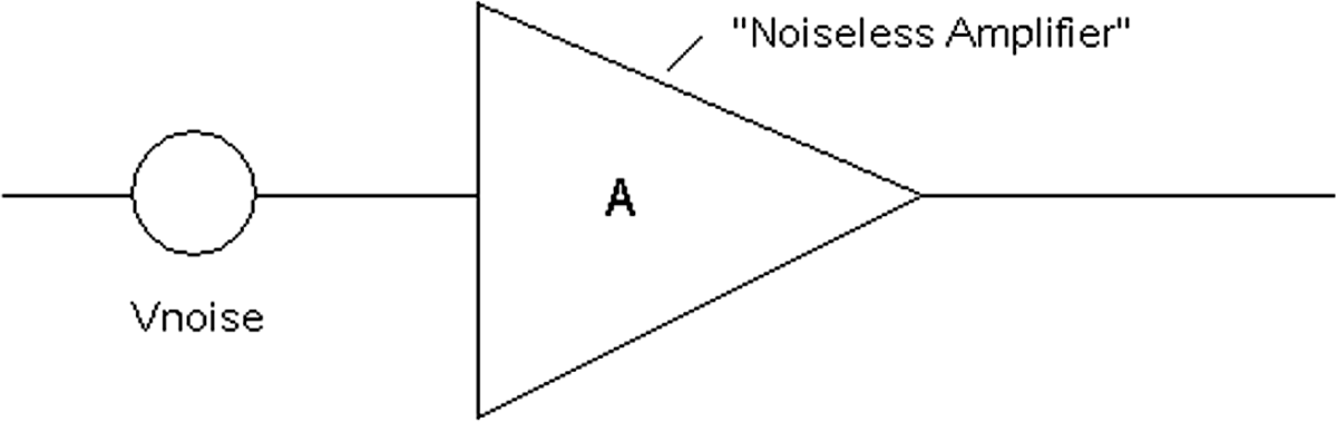
FIGURE 22-2 A model showing equivalent noise input voltage with a noisy input source connected to a “noiseless” amplifier.
This then means that to find an equivalent noise voltage at the input of the Phase Linear 700 amplifier, Equation (22-2) is used:
![]()
![]()
or
![]()
Figure 22-3 shows how to relate the equivalent input noise voltage into an equivalent input noise resistance, where the resistor generates Vnoise via Vnr = ![]() at the input of the amplifier. The equivalent noise resistance at the input is calculated by
at the input of the amplifier. The equivalent noise resistance at the input is calculated by
![]()
and then rearranging the terms to
![]()
for B = 20,000 Hz, as shown in Table 22-1 for the Phase Linear 700 amplifier, R = 72 k![]() = equivalent input noise resistance (as shown in Figure 22-3).
= equivalent input noise resistance (as shown in Figure 22-3).
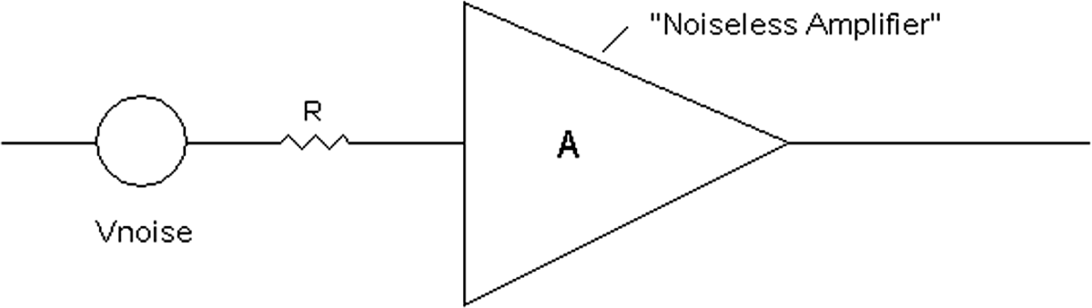
FIGURE 22-3 An equivalent input noise resistance model.
![]()
Although the input noise is a little high by today’s standards, the noise voltage at the output of the amplifier is really a combination of noise from resistors and transistors inside the amplifier. But still, the Phase Linear 700 amplifier’s SNR is 108.5 dB, and the SNR exceeds the dynamic range of 16-bit CD audio players today.
Another convenient way of calculating noise is to first set Vnr to ![]() = 1 nV for B = 1 Hz and find R. After some calculations, R = 61
= 1 nV for B = 1 Hz and find R. After some calculations, R = 61 ![]() for 1 nV of noise for B = 1 Hz. Then one can find the equivalent noise resistance for a given noise voltage density specification in Y nV/
for 1 nV of noise for B = 1 Hz. Then one can find the equivalent noise resistance for a given noise voltage density specification in Y nV/![]() , where Y is the scalar for nanovolts per (square) root hertz. Then
, where Y is the scalar for nanovolts per (square) root hertz. Then
Equivalent noise resistance = (Y2)61 ![]()
For example, a FET such as the 2N3382 has an equivalent input noise voltage density of 10 nV/![]() thus Y = 10, and the equivalent noise resistance is (Y2)61
thus Y = 10, and the equivalent noise resistance is (Y2)61 ![]() = (100)61
= (100)61 ![]() = 6,100
= 6,100 ![]() . In another example, a TL072 op amp has an equivalent input noise of 18 nV/
. In another example, a TL072 op amp has an equivalent input noise of 18 nV/![]() thus the equivalent noise resistance that the equivalent voltage generated by a resistor to provide 18 nV/
thus the equivalent noise resistance that the equivalent voltage generated by a resistor to provide 18 nV/![]() is (182)61
is (182)61 ![]() = 19.76 k
= 19.76 k![]() .
.
For active components such as transistors, the shot-noise generators exist as current noise generators across the collector and emitter and the base and the emitter. Figure 22-1B shows the shot-noise generators ICshot_noise and IBshot_noise. These two current-source generators are characterized by
![]()
where ICQ is the quiescent collector current, q is electron charge (= 1.6 × 10⁻¹⁹ Coulomb) and B is bandwidth in hertz.
![]()
where β = the current gain of the transistor and ![]() = IB is the base current.
= IB is the base current.
For a transistor direct-current (DC) collector current of 1 mA, and for a bandwidth of 1 Hz, the collector shot-noise current is ![]() Amp = 17.9 pA, and for a current gain β of 100, the base-current shot noise is 1.79 pA. Therefore, at a base current of 10 μA = IC/β = 0.001 mA/100, the noise current density is
Amp = 17.9 pA, and for a current gain β of 100, the base-current shot noise is 1.79 pA. Therefore, at a base current of 10 μA = IC/β = 0.001 mA/100, the noise current density is
![]()
A way to reflect the collector shot-noise current to the input is to find an equivalent input voltage that is amplified by the transconductance of the transistor to provide the same amount of collector noise current (Figure 22-4).
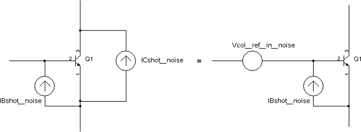
FIGURE 22-4 “Reflecting” the collector noise current source back to the input via an equivalent noise source.
So what we need is a noise voltage, which is the shot-noise current from the collector to the emitter expressed as a referred input voltage. This referred input noise voltage source is defined as Vcol_ref_in_noise such that
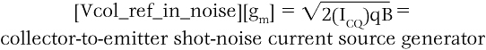
Let’s square both sides for now:
![]()
However,
![]()
![]()
Recall that the resistor noise is related to 4kTBR. If we use 1/gm as a resistor, Equation (22-8) almost fits the 4kTBR factor. So we just multiply the numerator and denominator by 1 = 2/2 to provide the following:

From Equation (22-9), the referred input noise voltage, Vcol_ref_in_noise looks like a noise voltage from a resistor of resistance value 1/2gm.
We can further express equivalently that there is an input referred noise resistance 1/2gm. In the analysis of noise, sometimes calculating the total noise resistance referred to the input allows the designer to evaluate the values of feedback resistors or voltage-source resistors.
Thus the equivalent input noise resistance is 1/2gm, where
![]()
where ICQ is the DC collector current. For a DC collector current of 1 mA, the equivalent input noise resistance that is referenced from the collector current shot noise generator then is
![]()
For 100 μA of collector current, the equivalent noise resistance is 130![]() , and for 10 μA of collector current, the equivalent noise resistance is 1,300
, and for 10 μA of collector current, the equivalent noise resistance is 1,300 ![]() .
.
Accordingly, from the preceding three example calculations, lowering the collector current actually results in more equivalent noise referred to the input. And increasing the collector current results in less equivalent noise referred to the input. However, with bipolar transistors, increasing the collector current also increases the base-current shot-noise-generator current source. Therefore, there is a tradeoff in terms of setting the collector current based on the source-driving resistance. At 1 mA of collector current and a β of 100, the base shot-noise current density is IBshot_noise_density = 1.79 pA/![]() . The noise voltage generated by the base noise current is just the source resistance multiplied by the base noise current, or the noise voltage density is equal to the base shot-noise current density multiplied by the source resistance (Figure 22-5).
. The noise voltage generated by the base noise current is just the source resistance multiplied by the base noise current, or the noise voltage density is equal to the base shot-noise current density multiplied by the source resistance (Figure 22-5).
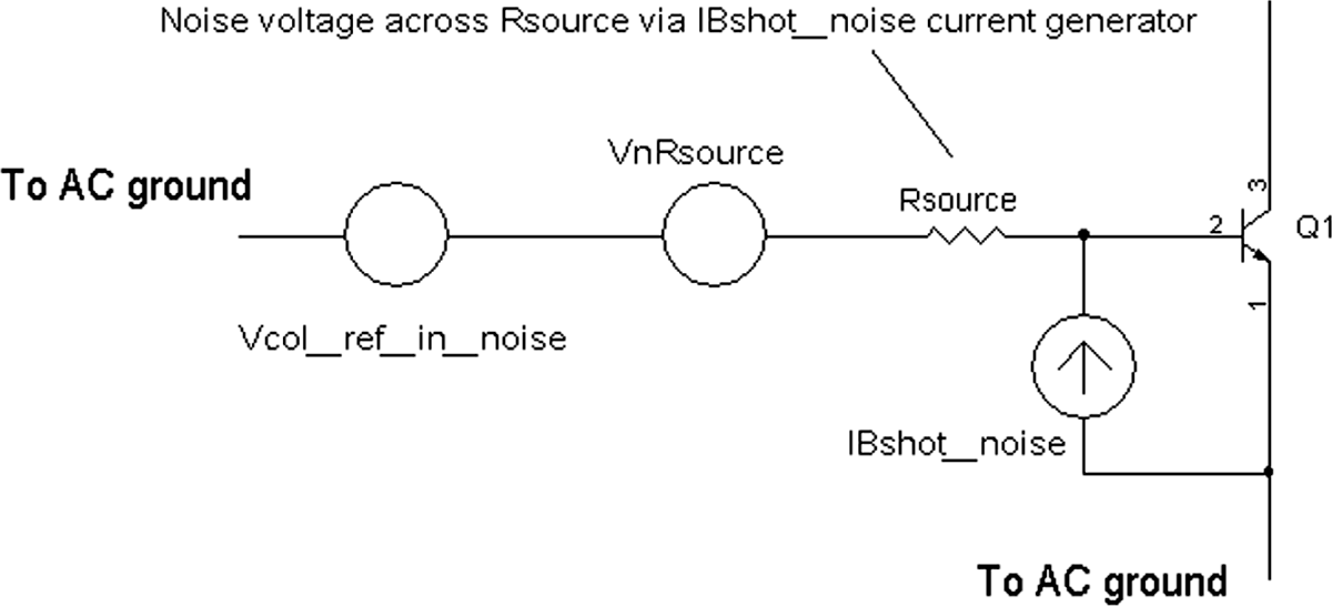
FIGURE 22-5 Base current shot-noise generator contributing to noise voltage via the input source resistor, Rsource.
For example, if the signal source resistance Rsource is less than a few hundred ohms, such as an RF 50-![]() or 75-
or 75-![]() source or a low-impedance microphone (<300 V), most likely the collector current can be set up to about 1 mA for a transistor current gain of 100. If the current gain is very high, such as a β of 300 or more, then the collector current in this example can be set higher to a few milliamps.
source or a low-impedance microphone (<300 V), most likely the collector current can be set up to about 1 mA for a transistor current gain of 100. If the current gain is very high, such as a β of 300 or more, then the collector current in this example can be set higher to a few milliamps.
At 1 mA with a β of 100, the base noise current has an IBshot_noise_density of 1.79 pA/![]() , and with Rsource at 300
, and with Rsource at 300 ![]() , the noise voltage density caused by base noise current is then 1.79 pA/
, the noise voltage density caused by base noise current is then 1.79 pA/![]() × 300
× 300 ![]() = 0.537 nV/
= 0.537 nV/![]() or the equivalent noise voltage generated from a 17.5-
or the equivalent noise voltage generated from a 17.5-![]() resistor [(0.5372)61
resistor [(0.5372)61 ![]() ], which is almost comparable with ½gm = 13
], which is almost comparable with ½gm = 13 ![]() , the equivalent input noise resistance from the collector shot-noise current generator.
, the equivalent input noise resistance from the collector shot-noise current generator.
Thus, with a perfect transistor, the total noise resistance referred to the input is the source resistance Rsource = 300 ![]() 17.5
17.5 ![]() 13
13 ![]() . The noise level is contributed substantially by the source resistance and not the transistor.
. The noise level is contributed substantially by the source resistance and not the transistor.
However, if the source resistance is increased to 10,000 ![]() , collector current is 1 mA, and a β is 100, the base current shot noise will provide 1.79 pA/
, collector current is 1 mA, and a β is 100, the base current shot noise will provide 1.79 pA/![]() × 10,000
× 10,000 ![]() = 17.9 pA/
= 17.9 pA/![]() or the equivalent noise resistance of (17.9)2 = 19.5 k
or the equivalent noise resistance of (17.9)2 = 19.5 k![]() . Therefore, the total input-referred resistance is 10,000
. Therefore, the total input-referred resistance is 10,000 ![]() 19,500
19,500 ![]() + 13
+ 13 ![]() . From this example, we can see that the base-current shot noise into the 10-k
. From this example, we can see that the base-current shot noise into the 10-k![]() source resistance generates most of the noise voltage. One solution is to select a transistor with a higher β (>100) such as a β = 300 to 800.
source resistance generates most of the noise voltage. One solution is to select a transistor with a higher β (>100) such as a β = 300 to 800.
However, a better alternative to designing a low-noise preamplifier with a medium to high signal source resistance (e.g., a parallel-tank circuit) is to use a low-noise JFET such as the 2SK152, J110, or LSK170. These JFETs have an equivalent input-noise voltage density of about 1.0 nV/![]() with negligible gate current.
with negligible gate current.
In the preceding example, the transistor was deemed to be perfect in the sense that there was no internal base series resistor Rbb (see Figure 22-1C). However, commercially made transistors include an internal base series resistor as a result of the process of making transistors. In general, typical base series resistors can be in the range of several hundred ohms to a thousand or more ohms. Certain low-noise, switching, or power transistors have Rbb < 50 ![]() . For low-noise applications, the commonly available PNP transistor 2N4403 has an Rbb in the 40-V range according to low-noise-amplifier expert John Curl. Note that PNP transistor 2N4403 has a little less noise than NPN versions 2N4400 and 2N4401.
. For low-noise applications, the commonly available PNP transistor 2N4403 has an Rbb in the 40-V range according to low-noise-amplifier expert John Curl. Note that PNP transistor 2N4403 has a little less noise than NPN versions 2N4400 and 2N4401.
Another very low-noise bipolar transistor is the Toshiba 2SA1316, rated at 0.60 nV/![]() , which has an equivalent input noise resistance of 22
, which has an equivalent input noise resistance of 22 ![]() , including the Rbb and the shot-noise components. The specification sheet states that the Rbb is about 2
, including the Rbb and the shot-noise components. The specification sheet states that the Rbb is about 2 ![]() for the 2SA1316. Some of the earlier “low-noise transistors,” such as NPN transistor 2N5089, have an Rbb in the area of about 1,000
for the 2SA1316. Some of the earlier “low-noise transistors,” such as NPN transistor 2N5089, have an Rbb in the area of about 1,000 ![]() , whereas its PNP counterpart, the 2N5087, does much better with an Rbb in the range of 200 to 300
, whereas its PNP counterpart, the 2N5087, does much better with an Rbb in the range of 200 to 300![]() . Other common low-noise NPN transistors, such as the PN2222 and PN2222A, have specified characteristics with comparable Rbb values (<50
. Other common low-noise NPN transistors, such as the PN2222 and PN2222A, have specified characteristics with comparable Rbb values (<50 ![]() ) to the 2N2N4401. And the data sheet for the PN2907A, its PNP transistor counterpart, has a similar noise performance as the 2N4403. However, the noise performance of transistors may vary from the specification sheet depending on the manufacturer, so transistors such as the PN2222, PN2222A, and PN2907A should be tested and verified for noise performance, according to John Curl.
) to the 2N2N4401. And the data sheet for the PN2907A, its PNP transistor counterpart, has a similar noise performance as the 2N4403. However, the noise performance of transistors may vary from the specification sheet depending on the manufacturer, so transistors such as the PN2222, PN2222A, and PN2907A should be tested and verified for noise performance, according to John Curl.
![]()
The PN2222(A) and PN2907A have their pin-outs reversed from 2N part-number transistors such as the 2N3904. Be careful to verify the pin-outs for the transistors starting out with PNxxxx.
Typical general-purpose transistors such as the 2N3904 or 2N4126 NPN transistors have Rbb values on the order of more than 500 ![]() , and most likely Rbb ≈ 1,000
, and most likely Rbb ≈ 1,000 ![]() . Their complementary PNP transistors, 2N3906 and 2N4126, fared much better, with Rbb ≈ 100 to 150
. Their complementary PNP transistors, 2N3906 and 2N4126, fared much better, with Rbb ≈ 100 to 150 ![]() or so. In general, the dominant noise source for a bipolar transistor results from the series base resistor. For example, the equivalent input noise resistor pertaining to collector current shot noise at 1 mA is 13
or so. In general, the dominant noise source for a bipolar transistor results from the series base resistor. For example, the equivalent input noise resistor pertaining to collector current shot noise at 1 mA is 13 ![]() , whereas the typical base series resistor, Rbb is typically greater, such as at least 50
, whereas the typical base series resistor, Rbb is typically greater, such as at least 50 ![]() .
.
Paralleling Transistors for Lower Noise
An alternative to lowering the noise effects of the series base resistor Rbb is to parallel transistors. I learned this paralleling transistor technique from John Curl and from his design of the JC-1 moving-coil pre-preamp. Generally, if the transistors are on the same package or die, paralleling them is not a problem. For discrete transistors to be paralleled, some combination of matching for the same VBE turn-on voltage between each transistor and/or using emitter resistors to help stabilize the biasing must be chosen. Otherwise, there will be an imbalance of collector currents, and one transistor can hog most of the desired collector current, leaving the other transistors at very low collector currents. For an example circuit that shows paralleling transistors for low-noise applications, go to www.google.com/patents and type in 4035737, which is U.S. Patent no. 4,035,737, inventor John Curl, filed on March 5, 1976. Also see Figure 22-6, a preamp circuit from U.S. Patent no. 4,035,737.
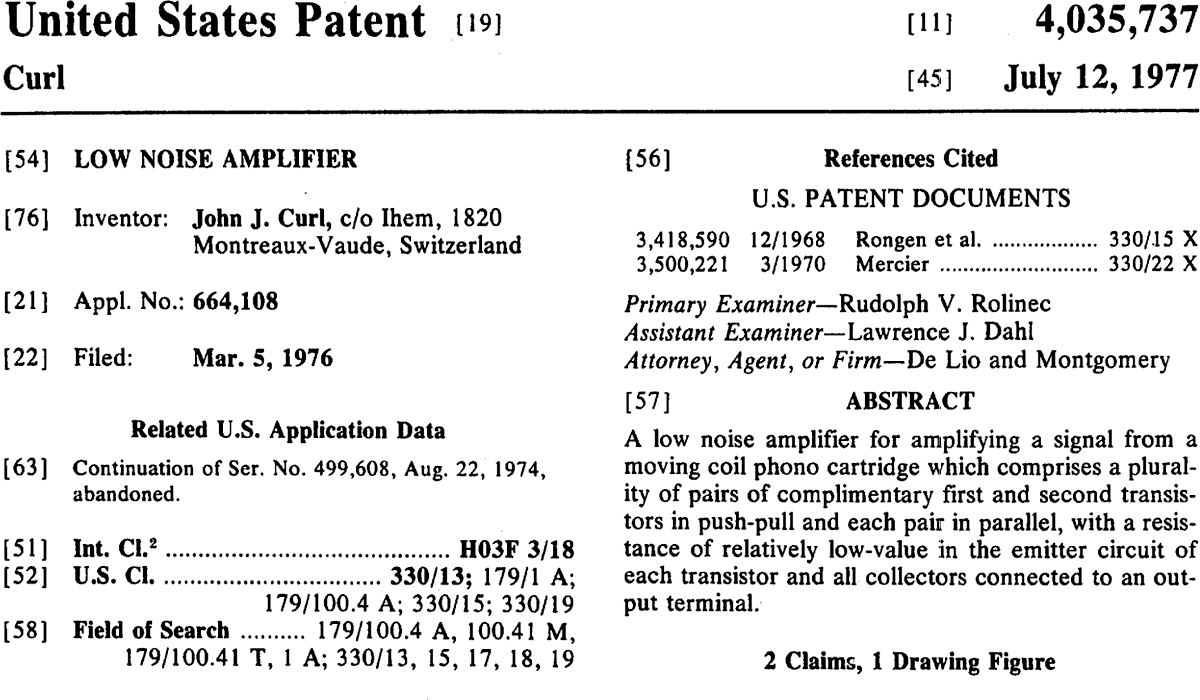
FIGURE 22-6 A low-noise preamplifier with paralleled transistors.
For audio situations, paralleling transistors for low-noise applications works very well. The “side effect” is increasing capacitance across the collector, base, and emitter terminals, but for audio, this is generally fine. The paralleled transistors also can be coupled at their collectors to a common-base amplifier to form a cascode circuit. In this way, the Miller effect is minimized, and for RF applications, the input capacitances of the paralleled transistors can be tuned or resonated with an inductor.
Note that paralleling JFETs also can lower noise as well. For example, in a 1973 Ampex BC-230 studio color television camera, three JFETs were paralleled for the camera tube preamplifier. The drains of the three FETs then were connected to the emitter of a grounded base amplifier to form a cascode preamplifier. Figure 22-7 shows a simplified circuit diagram of n bipolar transistors connected in parallel. The transistors are all matched in terms of VBE turn-on voltage.
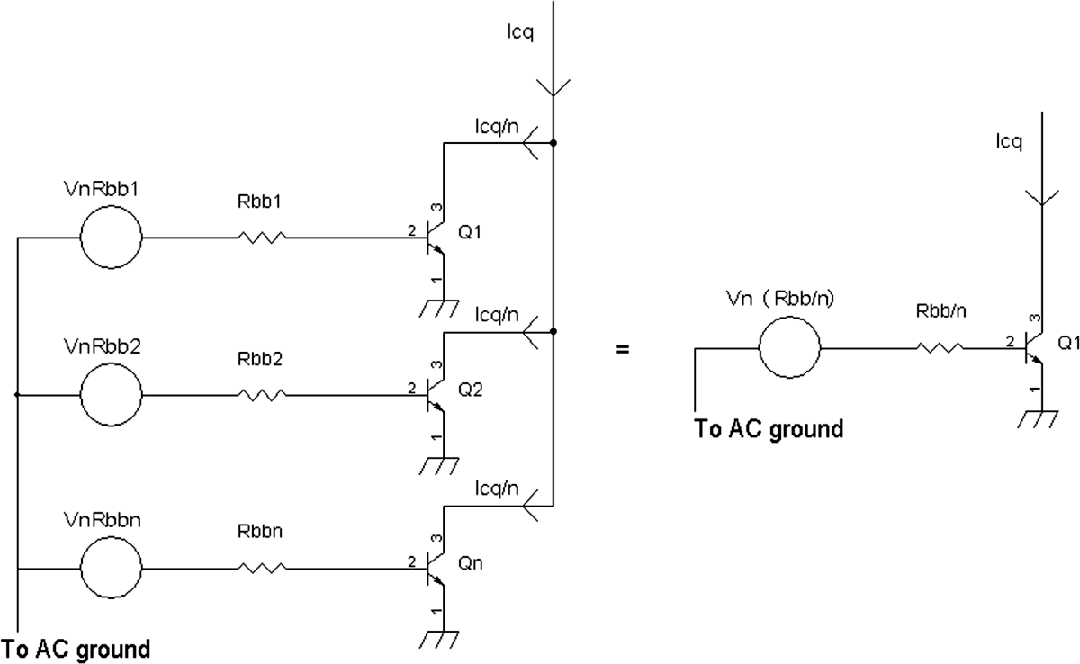
FIGURE 22-7 Multiple transistors paralleled with series base resistors to effectively reduce base resistance.
Figure 22-7 shows n transistors connected in parallel. For this analysis, the series base resistors Rbb1, Rbb2,…Rbbn all have the same resistance value. Thus Rbb1 = Rbb2… = Rbbn.
For a total DC collector current of ICQ where Icq is the sum of the quiescent collector currents for all the transistors Q1 to Qn, each transistor is operating at a DC collector current of Icq /n because there are n transistors, and the collector currents are evenly divided. Therefore, the transconductance of each transistor is gm/n, where gm is the tranconductance of a transistor operating at a collector current of Icq.
Also, for the analysis, the small signal input resistance of each transistor is β/(gm/n ) = n β/gm >> Rbb1. For example, if β = 100 and n = 2 with ICq = 1 mA, then n β/gm = 200/0.0384 mho = 5,200 ![]() . Typically, Rbb < 500
. Typically, Rbb < 500 ![]() , so the noise voltage formed by Rbb with Rbb in series is applied to the base emitter junction of the transistor with negligible loss. That is, the input resistance at the base of the transistor is typically much larger than Rbb.
, so the noise voltage formed by Rbb with Rbb in series is applied to the base emitter junction of the transistor with negligible loss. That is, the input resistance at the base of the transistor is typically much larger than Rbb.
The total noise from the n transistors thus is

![]()

![]()
from each series base resistor are independent random noise sources, squaring the sum of the noise voltages is just the sum of the squares of each noise voltage. That is, the independent sources are orthogonal such that each noise source can only multiply with itself to provide a finite number; other noise terms that multiply one noise source with a different independent noise source will amount to zero. And the square of
![]()
Therefore,

Let Rbb = Rbb1 = Rbb2 = …Rbbn because these are all the same resistance values. And since there are n series resistors,
![]()
Thus
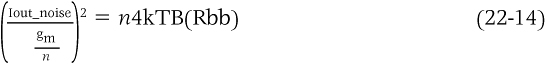

![]()
![]()
![]()
![]()
Note that gm = Icq/0.026 volt, where Icq is the summed DC collector currents of all n transistors.
Therefore, paralleling n transistors with each transistor having a series base resistor is equivalent to a single transistor with the series base resistor’s resistance divided by n.
Equation (22-19) thus represents the output noise current of a transistor that has a thermal noise voltage related to a series base resistor Rbb/n. See the right-hand side circuit of Figure 22-6. Therefore, the (series base resistor) noise voltage contributed by paralleling n transistors results in the noise of a single transistor multiplied by a factor of 1/![]() . For example, regarding noise from Rbb, paralleling four transistors or n = 4 results in 1/
. For example, regarding noise from Rbb, paralleling four transistors or n = 4 results in 1/![]() , the noise of a single transistor, or one-half the noise of a single transistor.
, the noise of a single transistor, or one-half the noise of a single transistor.
![]()
Note that the collector shot-noise current does not change when the transistors are paralleled, and it is still = ![]()
Differential-Pair Amplifier Noise
A differential-pair amplifier with no series emitter resistors gives about 3 dB (1.41 = ![]() ) more noise than a grounded emitter amplifier. The differential-pair amplifier compared with a grounded emitter amplifier has 1.41 more input referred noise voltage from the collector-to-emitter shot-noise current generators. If one factors in the series base resistors, in a differential-pair amplifier there is twice the series base resistance, which comes from a series base resistor from each of the two transistors. As a result of the two series base resistors in the differential-pair amplifier, the thermal noise generated by them yields 1.41 times the noise voltage from a single series base resistor of a grounded emitter amplifier. Recall that the thermal noise voltage has a square-root function of resistance (see Figures 22-8, 22-9, and 22-10).
) more noise than a grounded emitter amplifier. The differential-pair amplifier compared with a grounded emitter amplifier has 1.41 more input referred noise voltage from the collector-to-emitter shot-noise current generators. If one factors in the series base resistors, in a differential-pair amplifier there is twice the series base resistance, which comes from a series base resistor from each of the two transistors. As a result of the two series base resistors in the differential-pair amplifier, the thermal noise generated by them yields 1.41 times the noise voltage from a single series base resistor of a grounded emitter amplifier. Recall that the thermal noise voltage has a square-root function of resistance (see Figures 22-8, 22-9, and 22-10).
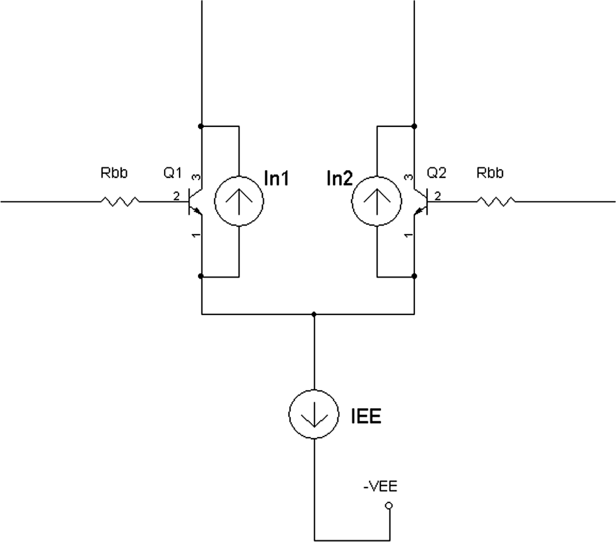
FIGURE 22-8 A differential-pair amplifier with collector-to-emitter shot-noise generators and series base resistors.
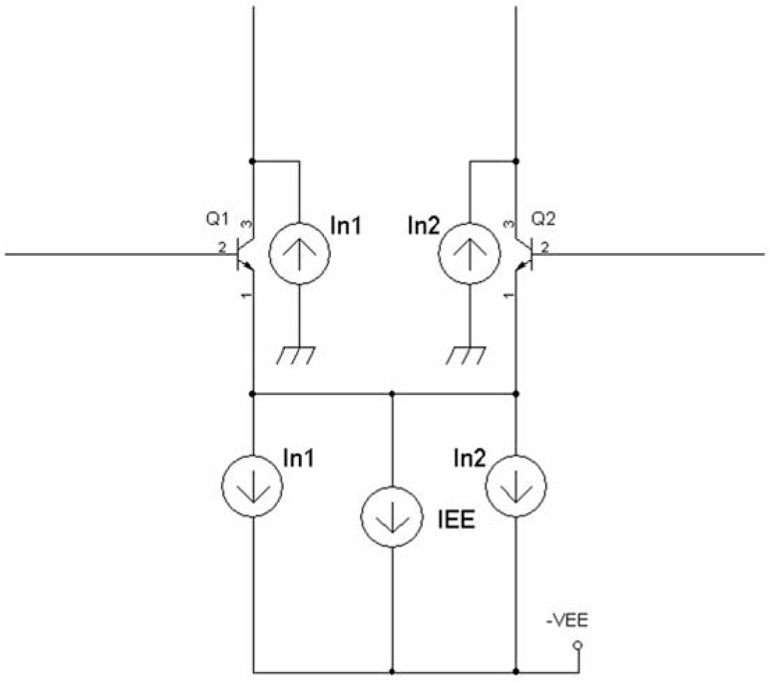
FIGURE 22-9 Collector-to-emitter shot-noise generators redrawn as current-source generators at the emitters and collectors of Q1 and Q2.
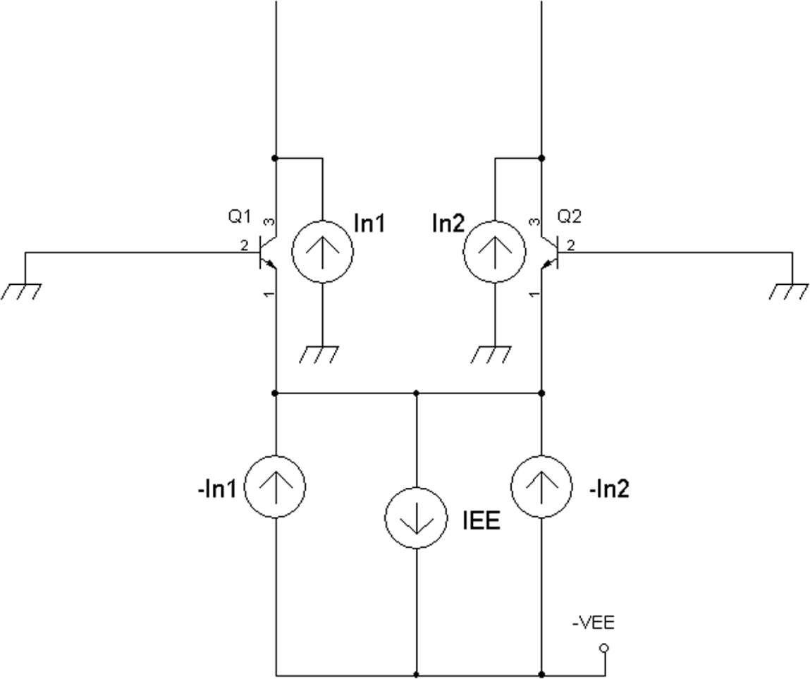
FIGURE 22-10 Collector-to-emitter shot-noise generators shown as opposing current sources at the emitters of Q1 and Q2.
Figure 22-8 shows a differential-pair amplifier with Q1 and Q2 transistors that have series base resistors Rbb1 and Rbb2 along with collector-to-emitter shot-noise generators In1 and In2. For the noise analysis, the base-current shot-noise components will be considered “small.” The signal source across the bases of Q1 and Q2 has sufficiently low source resistance that the base-current shot-noise generators are insignificant in the noise performance of the differential-pair amplifier.
Since Q1 and Q2 are matched transistors, the total series base resistance is just 2 × Rbb1 or 2 × Rbb2, twice the series base resistance, thereby increasing the thermal noise voltage by a single series base resistor Rbb, where Rbb = Rbb1 = Rbbb2. Thus
![]()
Thus, for noise owing to series base resistance, the differential-pair amplifier has twice the noise resistance of a single-ended grounded emitter amplifier.
Also seen in Figure 22-8 is the emitter DC current source IEE, that evenly divides the emitter currents for Q1 and Q2 when both bases are tied to the same voltage, such as a ground (0 V). For that matter, any current source connected to the emitters of Q1 and Q2 will have its current evenly split to half the current flowing out of the collector of Q1 and the other half flowing out of Q2, for a current gain of the transistors of β>> 10. Recall that for large β (>>10), the collector current is equal to the emitter current.
In Figure 22-8, the collector-to-base shot-noise generators In1 and In2 are “floating” in a sense that unlike the grounded emitter amplifier, where the collector-to-emitter noise current source is grounded at one end, the noise sources are not grounded in the differential-pair amplifier. For each transistor Q1 and Q2, there is a noise current source summing with the collector and the same noise current source flowing into the emitter of the respective transistor in an opposite direction (see Figure 22-9). For an analysis of the collector shot-noise current generators, the series base resistors have been omitted in Figures 22-9 and 22-10.
Thus Figure 22-9 shows each “floating” noise source as a combination of two current noise sources, one flowing noise current with the collector and another current noise source flowing in the opposite direction into the emitters. These two current sources are correlated, which means that they are not independent of each other, and their noise voltages add like other voltages. For example, The In1 noise current source at the collector will be partially canceled out by the In1 noise current source flowing into the emitter because the In1 noise current source flowing into the emitter is flowing in the opposite direction as the noise current source In1 at the collector. However, In1 and In2 are still independent of each other and add by the sum of the squares and then taking the square root (see Figure 22-10).
Figure 22-10 thus shows noise current sources flowing into the emitters of Q1 and Q2 as –In1 and –In2. The differential-pair amplifier is configured to evenly split both the emitter noise current sources (–In1 and –In2) in half going to the collectors of Q1 and Q2. To analyze shot-noise components and refer them back to the input of the differential-pair amplifier as an equivalent input noise voltage, see Figure 22-10.
Therefore, the total noise current at the collector of Q1 is
![]()
and the total noise current at the collector of Q2 is
![]()
Because the shot-noise currents In1 and In2 are independent sources,
![]()
and,
![]()
![]()
and
![]()
![]()
Icq = quiescent collector current of Q1 = quiescent collector current of Q2.

and

To find the equivalent input noise owing to shot-noise current generators from Q1 and Q2, we have
![]()
Then
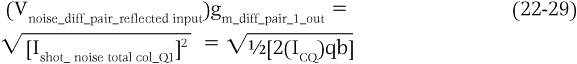
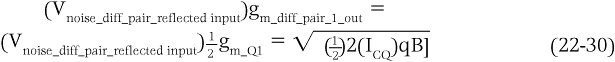
However, gm_diff_pair_1_out = (½)gm_Q1 because the transconductance of a differential-pair amplifier is reduced by half as a result of the output signal being taken at one collector output.
![]()
If the output signal is taken differentially from the collector of Q1 and the collector of Q2, then gm_diff_pair_1_out = gm_Q1.
Therefore,
Squaring both sides of the equation yields
![]()
![]()
Multiplying by 4 on both sides, we get
![]()
![]()
But
![]()
so
![]()
When the square root is taken on both sides,
![]()
Equation (22-36) relates to an equivalent input noise resistance of 1/gm_Q1, which is twice the input noise resistance of a single-ended ground emitter amplifier whose equivalent input noise resistance is 1/2gm, as shown in Equation (22-9). Thus, for the same collector current, a differential-pair amplifier has twice the equivalent noise resistance at the input than a single-ended grounded emitter amplifier pertaining to shot-noise currents across the collector to the emitter. This twice noise resistance thus relates to an equivalent input noise voltage of 1.41 or = ![]() of the equivalent input noise voltage of the grounded emitter amplifier in terms of shot noise.
of the equivalent input noise voltage of the grounded emitter amplifier in terms of shot noise.
In practice, since there is also an extra series base resistor in the differential-pair amplifier, the equivalent input noise in a differential amplifier is increased by 1.41 owing to both shot noise and series base resistors over a single-ended grounded emitter amplifier.
Before we leave the noise analysis for a differential-pair amplifier, what if we take the output differentially from the collectors of Q1 and Q2 in Figure 22-10? Would the equivalent input noise due to the shot noise currents In1 and In2 for a differential output be different from a single ended output? The answer is no, the equivalent input noise is still the same for both cases. That is, the noise currents taken differentially at the outputs will be
![]()
or
![]()
Thus the noise current is increased by a factor of 2 when taken differentially as opposed to being taken from a single-ended output. The reason why the output noise current is increased by 2 and not by = ![]() is because the collector noise currents from Q1 and Q2 are correlated but out of phase. Also see equations (22-21) and (22-22) for the shot noise from the collector of Q1 and Q2, single ended output.
is because the collector noise currents from Q1 and Q2 are correlated but out of phase. Also see equations (22-21) and (22-22) for the shot noise from the collector of Q1 and Q2, single ended output.
However, the transconductance also increases by a factor of 2 in a differential-pair amplifier when the two output currents from Q1 and Q2 are taken differentially as opposed to an output current taken in a single-ended manner (e.g., collector current from either Q1 or Q2). Note that the equivalent input noise voltage is the ratio of the output noise current to the transconductance of the differential-pair amplifier. So, therefore, although the noise increases by a factor of 2 (in differential mode), so does the transconductance (in differential mode), which results in no change in equivalent input noise between the differential mode output and the single ended output.
Typically, the main contribution to noise in a differential-pair amplifier is the series base resistor for Q1 and Q2. Therefore, to lower noise in a differential-pair amplifier, one can use the technique of paralleling transistors. For example, Q1 and Q2 would consist of multiple paralleled, matched transistors.
Cascode Amplifier Noise
In a cascode amplifier, most of the noise is contributed by the common-emitter stage or bottom transistor (Q1). The top transistor or common-base transistor amplifier (Q2) contributes negligible amounts of noise. Figure 22-11 shows the noise sources for a cascode amplifier.
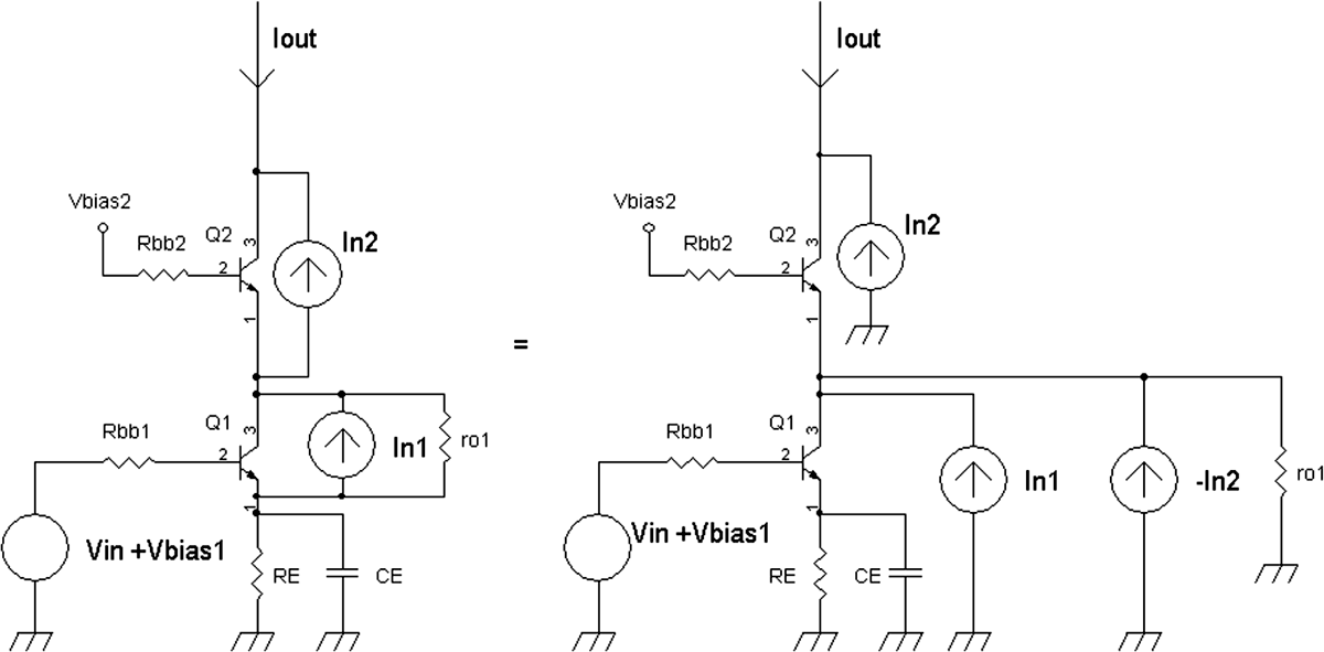
FIGURE 22-11 Cascode amplifier with thermal and shot-noise sources.
Figure 22-11 shows series base resistors Rbb1 and Rbb2 for the common-emitter amplifier Q1 and common-base amplifier Q2. Because the emitter of Q2 is loading into a current source Q1 with very high output resistance, the series base resistor of Q2 does generate a noise signal at the collector of Q2. When there is a noise voltage at the base of Q2, the emitter of Q2 is loaded to ground by the output resistance of Q1 r01, which does not contribute noise. Thus r01 is an emitter resistor to ground for Q2, and r01 is a local feedback resistor that lowers the transconductance in terms of Q2 for voltage at the base of Q2 and output current at the base of Q2. Typically, r01 > 10 k![]() .
.
The transconductance from the viewpoint of a noise voltage at the base of Q2 then is
Therefore, noise voltages at the base of Q2 do not appear at the output of Q2’s collector terminal. If there are appreciable capacitances from the emitter of Q2 to ground, then there will be a noise contribution from the noise voltage at the base of Q2. But generally at lower frequencies, this is not the case.
In terms of shot-noise contribution from the collector to the emitter of Q2, the shot-noise current generator In2 cancels out at the output of Q2’s collector. That is, at Q2’s collector, there is In2, but at Q2’s emitter, there is -In2. Since the emitter current is the same as the collector current for a large current gain β(>>1) of Q2, the -In2 noise-current source appears at the collector of Q2 and sums with the In2 noise source to cancel noise related to Q2.
Therefore, most of the noise in a cascode amplifier comes from the noise sources of the bottom transistor Q1. The series base resistor noise and the shot noise from the collector to the emitter of Q1 appear at the output of Q2 because the collector current of Q1 equals the collector current of Q2 for the current gain β >> 1 of Q2. Intuitively, it makes sense that the main noise contributions in a cascode amplifier come from the bottom transistor because it is the collector current of Q1 that “controls” the collector current of Q2.
Selecting Op Amps
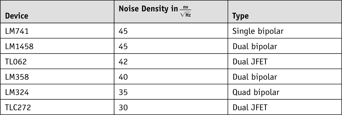
In terms of selecting for low-noise to ultralow-noise op amps, see Table 22-2.
TABLE 22-2 Equivalent Input Noise Densities for Low Noise Op Amps

Table 22-3 illustrates the noise performance of some general-purpose op amps.
TABLE 22-3 Equivalent Noise Densities for General Purpose Op Amps
To maintain noise performance with op amps, the selection of feedback resistor values is important. High-value resistors generally degrade noise performance (see Figure 22-12).
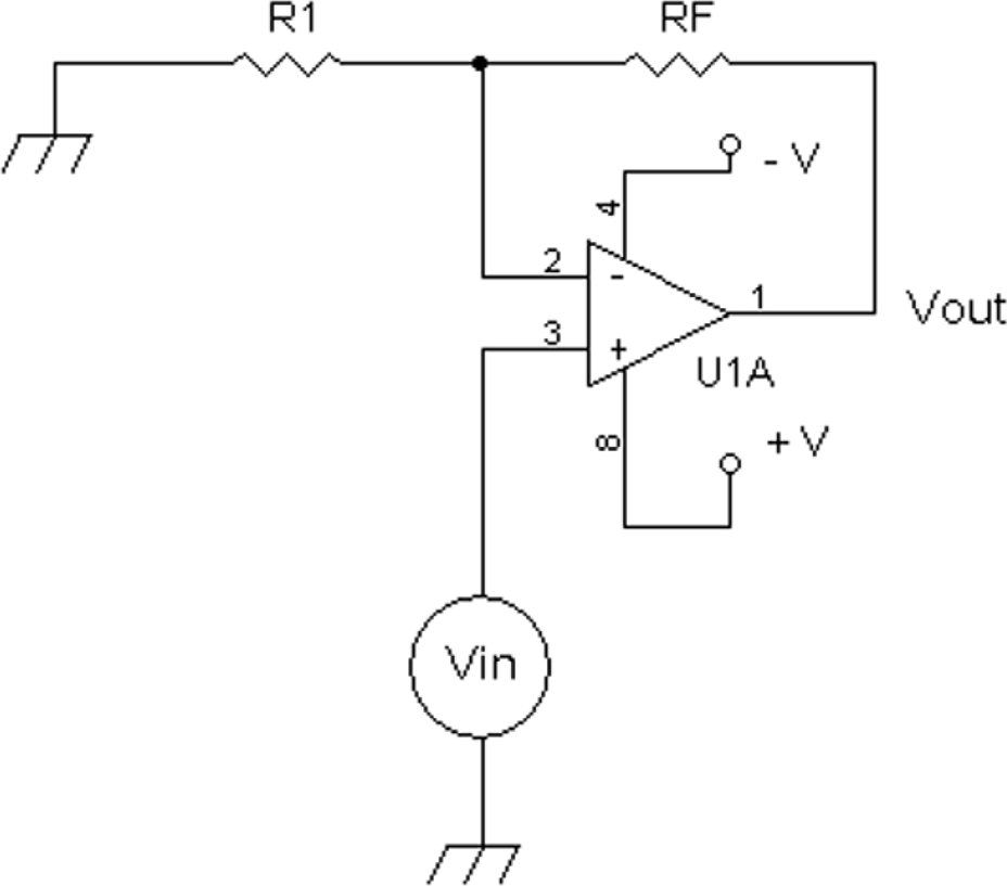
FIGURE 22-12 A noninverting amplifier.
Generally, a rule of thumb is to have the parallel combination of R1 and RF = (R1 × RF)/(R1 + RF) maintain the low noise capability of the op amp by having
![]()
where Y nV/![]() and Y is the scalar for nanovolts per square root of hertz. Then
and Y is the scalar for nanovolts per square root of hertz. Then
Equivalent noise resistance = (Y2)61 ![]()
For example, if the gain is greater than 10 and RF >> R1, then (R1 × RF)/(R1 + RF) ≈ R1, and if an AD797 op amp is chosen, then the equivalent noise resistance is (0.92)61 ![]() = 49
= 49 ![]() , which means that R1 < 24.5
, which means that R1 < 24.5 ![]() . Once the gain is known, the value of RF can be determined. For example, for a noninverting gain of 100, RF = 99(R1), where the gain = (R1 + RF)/R1.
. Once the gain is known, the value of RF can be determined. For example, for a noninverting gain of 100, RF = 99(R1), where the gain = (R1 + RF)/R1.
Under the same conditions of gain > 10, if an RC4558 is selected, then the equivalent noise resistance is (82)61 ![]() = 3,900
= 3,900 ![]() , which means that R1 < 1,850
, which means that R1 < 1,850 ![]() . Again, the value of RF can be determined when the gain = (R1 + RF)/R1 is known.
. Again, the value of RF can be determined when the gain = (R1 + RF)/R1 is known.
References
1. Class Notes EE141, Paul R. Gray and Robert G. Meyer, UC Berkeley, Spring 1975.
2. Class Notes EE241, Paul R. Gray and Robert G. Meyer, UC Berkeley, Fall 1975.
3. Class Notes EE140, Robert G. Meyer, UC Berkeley, Fall 1975.
4. Class Notes EE240, Robert G. Meyer, UC Berkeley, Spring 1976.
5. Paul R. Gray and Robert G. Meyer, Analysis and Design of Analog Integrated Circuits, 3rd ed. New York: John Wiley & Sons, 1993.
6. Kenneth K. Clarke and Donald T. Hess, Communication Circuits: Analysis and Design. Reading: Addison-Wesley, 1971.
7. National Semiconductor, Audio/Radio Handbook. Santa Clara: National Semiconductor Corporation, 1980.
8. R. E. Zeimer and W. H. Tranter, Principles of Communications. Boston: Houghton Mifflin Company, 1976.
9. William G. Oldham and Steven E. Schwarz, An Introduction to Electronics. New York: Holt, Reinhart and Winston, Inc., 1972.
10. Allan R. Hambley, Electrical Engineering Principles and Applications, 2nd ed. Upper Saddle River: Prentice Hall, 2002.
11. Texas Instruments, Linear Circuits Amplifiers, Comparators, and Special Functions, Data Book 1. Dallas: Texas Instruments, 1989.
12. Motorola Semiconductor Products, Inc., Linear Integrated Circuits, Vol. 6, Series B., 1976.
13. Thomas M. Frederiksen, Intuitive IC Op Amps from Basics to Useful Applications (National’s Semiconductor Technology Series). Santa Clara: National Semiconductor Corporation, 1984.
14. Alan B. Grebene, Bipolar and MOS Analog Circuit Design. New York: John Wiley & Sons, 1984.
15. U.S. Patent 4,035,737, “Low-Noise Amplifier,” John J. Curl, filed on March 5, 1976.
16. U.S. Patent 5,471,531, “Method and Apparatus for Low-Cost Audio Scrambling and Descrambling,” Ronald Quan, filed on December 14, 1993.
17. U.S. Patent 4,963,764, “Low-Noise Current Mirror Active Load Circuit,” Ronald Quan, filed on March 23, 1989.
18. U.S. Patent 6,617,910, “Low-Noise Analog Multiplier Utilizing Nonlinear Local Feedback Elements,” Ronald Quan, filed on August 10, 2001.
19. High Fidelity’s Test Reports. Great Barrington: Billboard Publications, Inc., 1973.
20. High Fidelity. New York: ABC Consumer Magazines, Inc. May 1987, pgs. 20–21.
21. Home Theater. New York: Source Interlink Media,), December 2009, pgs. 60–62.
22. Victor Company of Japan, Ltd., JVC Service Manual HR-D140U. Elmwood Park: JVC Company of America, 1985.