Chapter 11
Digital Upconversion and Downconversion
Abstract
Digital upconversion is the process of moving the frequency content of a baseband signal to a much high frequency. Digital downconversion is the opposite process. The process is described intuitively as well as mathematically using previously developed concepts. In addition, the role of analog-to-digital convertor and digital-to-analog convertor in this process is discussed.
Keywords
Baseband; Downconversion; Intermediate frequency; Sinc compensation; Upconversion
Previously, we talked about complex modulation and baseband signals. The whole point of this is to create a signal that can be used to carry the information bits from one location to another, whether over copper wire, a fiber optic cable, or electromagnetically through the air. In nearly all cases, the signal needs to ride on a carrier frequency to be efficiently sent from one location to another. To do this, the signal frequency spectrum needs the ability to be moved up and down the frequency axis, at will. This is a process of up and down (frequency) conversion. All early methods used analog circuits to accomplish this. In the last couple of decades, digital circuits, particularly FPGAs, have developed the computational capacity to perform these functions in many cases and offer important advantages over analog methods. This is known as digital upconversion and downconversion (also known by acronyms of DUC and DDC within the industry).
The process of upconversion is to take a signal that is at baseband (this means the frequency representation of the signal) and move or shift that frequency spectrum up to a carrier frequency. The width of the signal's frequency spectrum does not change; it is just moved to another part of the frequency spectrum. One common area of confusion is what happens to the negative part of the frequency spectrum. In a baseband signal, the negative frequency components overlay the positive components. Positive and negative frequencies are distinguished using complex representation. When the signal is upconverted, the positive and negative components are “unfolded” from on top of each, with the negative components below the carrier and the positive components above the carrier frequency.
A common example is speech. When you speak into a microphone, the sound waves create an electrical baseband signal, with frequency content from near 0 to about 3 kHz. With music, the frequency range can be much greater, up to 20 kHz. When we hear, the vibrations our ears detect are within this frequency range (in fact, our ears cannot hear frequencies beyond this range). This signal can be sampled and converted into a digital baseband signal or remain as an analog signal. To transmit this signal over the air using electromagnetic radio waves, the frequency needs to be increased. For example, the commercial AM radio system in the United States operates between 540 and 1600 kHz. The baseband speech signal is multiplied, or “mixed” with the much higher frequency carrier signal. This process superimposes the baseband signal on top of the carrier. For example, if the carrier frequency is 600 kHz, the upconverted 3 kHz speech signal will now ideally have a frequency or spectral content between 600 − 3 and 600 + 3 kHz. This process also allows for multiple users to transmit and receive signals simultaneously, as each user can be assigned a different carrier frequency, and occupy different portions of the frequency spectrum. The up and downconversion process can place the baseband signal at any desired “channel” frequency, allowing many different signals to occupy a common frequency band or range without interference. In the AM radio example, the carrier frequencies are spaced 10 kHz apart. This frequency separation is sufficient to prevent interference between stations.
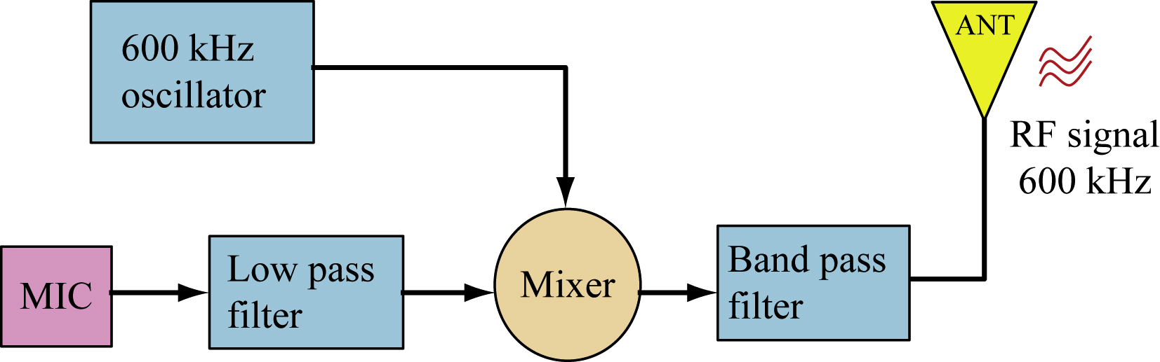
The process of mixing a baseband signal onto a carrier frequency is called upconversion and is performed in the radio transmitter. In the radio receiver, the signal is brought back down to baseband in a process called downconversion. Traditionally, this up and downconversion process was done using analog signals and analog circuits. Analog upconversion with real (not complex) signals is depicted in Fig. 11.1 below.
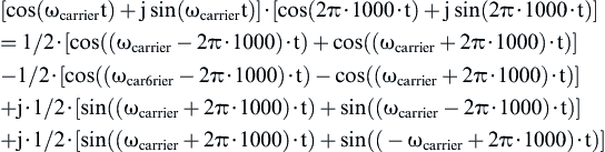
To see why a mixer works, let us consider a simple baseband signal of 1 kHz tone and a carrier frequency of 600 kHz. Each can be represented as a sinusoid. A real signal, such as a baseband cosine, has both a positive and negative frequency component. At baseband, these overlay each other, so this is not obvious. But once upconverted, the two components can be readily seen both above and below the carrier frequency.
The equation for the upconversion mixer is
or
The result is two tones, of half amplitude, at 599 and 601 kHz.
11.1. Digital Upconversion
Alternately, this process can also be done digitally. Let us assume that the information content, whether it is voice, music, or data, is in a sampled digital form. In fact, as we covered in the earlier chapter on modulation, this digital signal is often in a complex constellation form, such as QPSK or QAM, for example.
To transmit this information signal, at some point, it must be converted to analog domain. In the past, the conversion from digital to analog occurred while the signal was in baseband form, because the data converters could not handle higher frequencies. As the speeds and capabilities of analog-to-digital converters (ADC) and digital-to-analog converters (DAC) improved, it has became possible to perform the up and downconversion digitally, using a digital carrier frequency. The upconverted signal, which has much higher frequency content, can then be converted to analog form using a high speed DAC.
Upconversion is accomplished by multiplying the complex baseband signal (with I and Q quadrature signals) with a complex exponential of frequency equal to the desired carrier frequency.
The complex carrier sinusoid can be generated using a lookup table, or implemented using any circuit capable of generating two sampled sinusoids offset by 90°degrees (Fig. 11.2). To do this digitally, the sample rates of the baseband and carrier sinusoid signal must be equal. Since the carrier signal will usually be of much higher frequency than the baseband signal, the baseband signal will have to be interpolated, or upsampled, to match the sample frequency of the carrier signal. Then the mixing or upconversion process will result in the frequency spectrum shift depicted in Fig. 11.3 below.
To simplify things, let us assume the output of the modulator is a complex sinusoid of 1 kHz. The equation for this upconversion process is
After simplifying, this becomes
We can discard the imaginary portion. It is not needed because at carrier frequencies, both positive and negative baseband frequency components can be represented by spectrum above and below the carrier frequency.
The final result at the output of the DAC is
Note that there is only a frequency component above the carrier frequency. This is because the input was a complex sinusoid rotating in the positive (counterclockwise) direction—there was no negative frequency component in this baseband signal.


Normally, baseband signal will have both positive and negative frequency components. For example, the complex QPSK modulator output can jump both clockwise and counterclockwise depending upon the input data sequence. When upconverted, the positive and negative baseband components will no longer overlay each other, but be unfolded on either side of the carrier frequency. The baseband signal with a frequency spectrum of 0–10 kHz will occupy a total of 20 kHz, with 10 kHz on either side of the carrier frequency. But keep in mind that the baseband signal represents the positive and negative frequencies using quadrature form, so it is in the form of an I and Q signal, each with a frequency spectrum from 0 to 10 kHz.
Frequently, there are several steps in upconverting to the final frequency used for transmission, as shown in Fig. 11.4. There are several advantages in upconverting in steps, which is known as superheterodyne. Generally, the DAC must operate at least 2 ½ times the carrier frequency. For signals in the GHz range, this exceeds the capacity of most DACs (although very high performance DACs can now operate at several GHz conversion rates). Another consideration is filtering. If several upconverting steps are used, filtering can be applied at each step. Often, multiple stages of filtering are required to meet the system requirements in terms of meeting the spectral emission requirements in the transmitted RF signal, to ensure no interference with other users. A typical digital upconverting circuits is shown below (Fig 11.4).

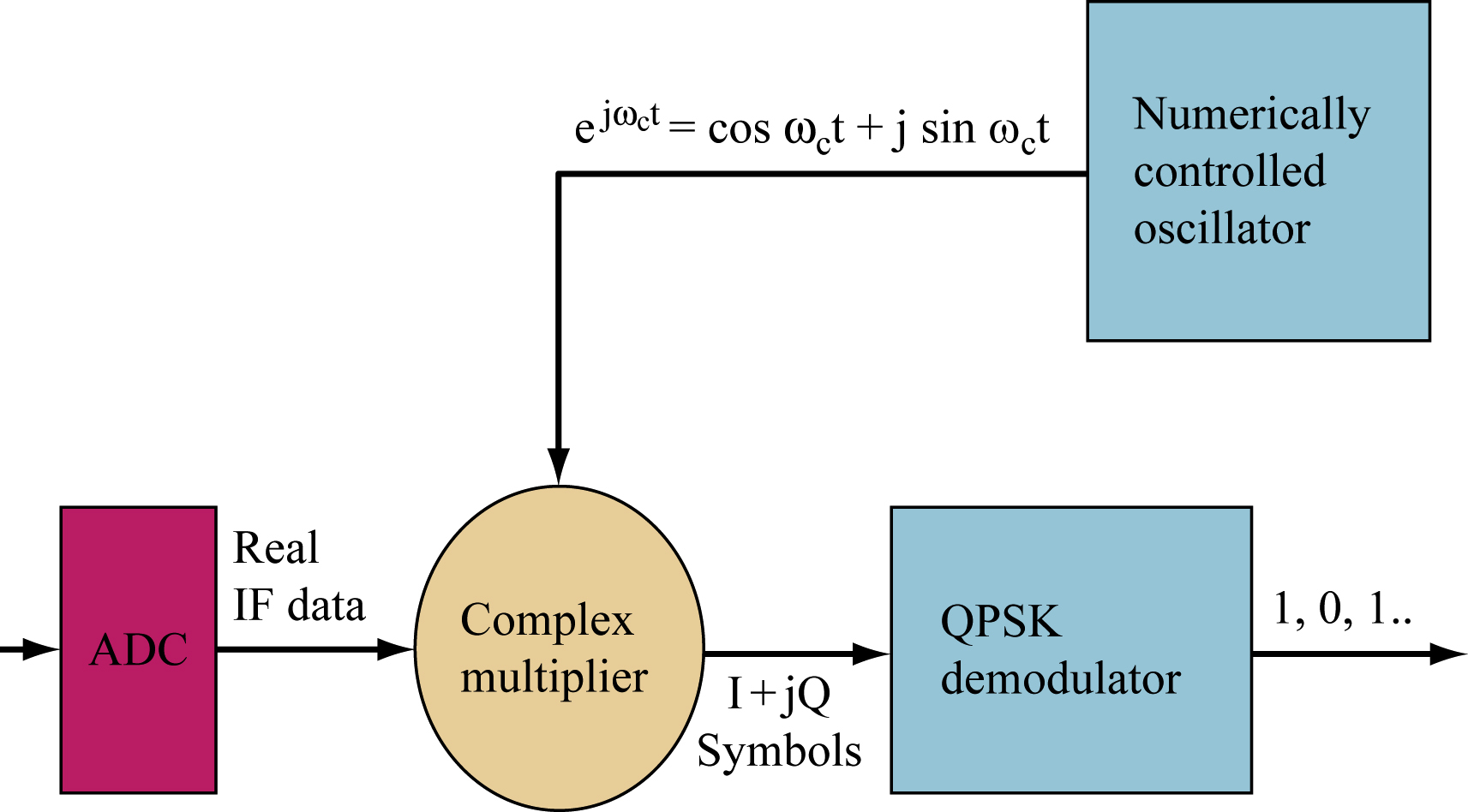
11.2. Digital Downconversion
Digital downconversion is the opposite of upconversion. The circuit diagram looks similar (Fig 11.5).
Digital downconversion involves sampling, so naturally aliasing needs to be considered. The Nyquist sampling rule states that the sampling frequency must be at least twice the highest frequency of signal being sampled. In practice, usually the sampling frequency is at least 2 ½ times the rate of signal frequency, to allow extra margin for the transition band of the digital low-pass filters following.
But this is not quite true. It is possible to sample a signal at frequency lower than its carrier frequency. The Nyquist rule applies to the actual bandwidth of the signal, not the frequency of the carrier.
11.3. Intermediate Frequency Subsampling
Using a technique called intermediate frequency (IF) subsampling, it is possible to sample at a much lower frequency than the carrier frequency. The term IF subsampling is used, as the frequencies typically used in this technique lie somewhere between baseband and RF. The term “IF” refers to intermediate frequency. In this case, we are going to deliberately take advantage of an alias of the signal of interest. This is best illustrated using an example.
We will use a 4G (fourth generation) wireless example. The signal of interest lies at 2500 MHz. Analog circuits are used to downconvert the signal to an IF or intermediate frequency. We will assume that we have an ADC sampling at 200 MHz. Further, let us also assume we have 20 MHz BW IF signal centered at 60 MHz in Fig. 11.6, which we are trying to sample and downconvert for baseband processing. By the Nyquist rule, we can sample up to ½ the sample rate, or 100 MHz. To allow easier postsampling filtering, we may want to limit this to 80 MHz instead. Our signal here lies between 50 and 70 MHz, so these conditions are met.


This should be familiar from the chapter on sampling. Now, let us consider what happens if the IF signal is centered at 460 MHz in Fig. 11.7, rather than 60 MHz.
As we discussed in the earlier chapter on sampling and aliasing, there is no way to distinguish between a signal and an alias at a multiple of the sample frequency. When IF subsampling is performed, this aliasing can be used to our advantage.
In our examples, any signal that aliases to a baseband frequency from −80 MHz to +80 MHz can work. Remember, the digital downconversion multiplies by a complex exponential, which can be rotating either counterclockwise or negative, thereby either shifting the spectrum left or right. Below in Fig. 11.8 is another example, showing downconversion from 340 MHz carrier frequency.
The signal at 340 MHz will be aliased as if it was at −60 MHz, and then can be shifted to baseband (the complex NCO runs in opposite rotational direction, to shift alias to right instead of left). The only areas of the spectrum that cannot be properly aliased down are those which alias to the region near the Nyquist frequency, in our case, 100 MHz. So signals close to 300, 500, and 700 MHz cannot be sampled in this way. But the rest of the spectrum can be sampled, so long as the sampling frequency meets the requirement of being more than twice the bandwidth of the signal of interest. In practice, the sampling frequency is often much higher than the signal bandwidth, which offers the additional advantage of allowing an increase in signal to noise ratio (SNR) when the baseband signal is decimated to a lower frequency for baseband processing.

In our example, the downconverted signal has a spectrum from −10 to +10 MHz. This requires a sampling frequency of at least 20 MHz for both I and Q. If a decimate-by-four finite impulse response (FIR) filter is used to low-pass filter the downconverted signal, and then further complex symbol processing can take place at 25 MHz. By sampling at a much higher rate and then low-pass filtering, a much greater percentage of the sampling quantization noise can be eliminated. Quantization noise, as discussed in an earlier chapter, is due to the effect of the signal being sampled and mapped to specific amplitude levels, which is limited by how many bits of resolution are available in the ADC. This noise is broadband, meaning that is distributed evenly across the frequency spectrum. The effect of the low-pass filter is to attenuate much of this quantization sampling noise, along with unwanted signals, in the stopband region. The net effect is the equivalent of adding 1 bit of precision or 6 dB to the SNR, for every factor of two in decimation and filtering.
In our example, if we used a 12-bit ADC at 200 MHz Fs, and performed the digital downconversion, low-pass filtering and decimate by four, it is the equivalent as if we had sampled at 50 MHz Fs using a 14-bit ADC. The decimation filter has in essence added 2 bits of resolution to the ADC, or 12 dB to the SNR of the sampled signal. This concept can be taken to extremes. There is a class of ADCs, called sigma-delta converters, which run at very high frequencies relative to the signal they are sampling, but only use a 1 bit sampler. An effective 10 or 12 bit ADC can be built using a single-bit sampling front end running at extremely high frequencies followed by decimation filtering stages.
Now let us go back to IF subsampling. In theory, one could sample a signal at any arbitrary frequency, but there must be some practical limitations. So far, we have only discussed the limitation of not sampling signals that alias to near the Nyquist frequency. But there are other limitations, and we will discuss two of these.
First, one must consider the performance of the ADC. There are two principle characteristics that are of concern here. Of course, the first is the maximum sampling rate at which the ADC operates. In our example, we assumed an ADC that could sample at 200 MHz. When IF subsampling, we must also consider the analog bandwidth of the sampling circuit in the ADC. Ideally, the ADC samples the signal for an infinitely small instant of time and converts that measurement into a digital number. In practice, this circuit has a sampling window or period of time in which it samples. The narrower this window, the higher signal frequencies it can sample. This specification is given in the data sheets provided by ADC manufacturers. In our example, we sampled a signal at 460 MHz. So we should check that our ADC has an analog front end bandwidth of 500 MHz or higher.
Another factor that must be considered is clock jitter. Clock jitter is the amount of timing variability of the edge of the ADC sampling clock from cycle to cycle. It can be readily seen on an oscilloscope of sufficient quality. It is more easily seen as clock phase noise on a spectrum analyzer. Jitter shows up as spectral noise tapering off on either side of the clock frequency component. The less jitter, the more closely the clock appears as simply a vertical line in the frequency response. The effect of clock jitter will be proportional to the frequency of the signal being sampled. It will limit the SNR according to the following relationship.
An example may make this clearer. In our example, the ADC clock was 200 MHz, which has a period of 5 nanoseconds (ns). Let us assume this clock has jitter of 5 picoseconds (ps). This does not sound like too much—only 0.1% of the clock period. First we will compute the SNR limitation due to clock jitter with an input signal at 60 MHz and then with at 460 MHz.
60 MHz IF signal:
460 MHz IF signal:
This level of clock jitter will limit the ADC performance for a 60 MHz signal at any level of precision beyond 10 bits. For a 460 MHz signal, the clock jitter will limit the SNR to 36 dB, or about 6 bits. Clearly, this level of clock jitter is excessive in this IF subsampling application.
An analogy can be the same strobe light concept used in the Sampling and Aliasing chapter. The strobe light is assumed to flash at exact intervals. Any variance, or jitter, in the flashing intervals, will cause distortion in the position of the red dot on the wheel. The IF subsampling process would be as if the wheel made multiple rotations between strobe flashs, though it would appear that the wheel was rotating at a slower speed. But as the wheel is actually rotating much faster, any sampling errors due to jitter in the strobe flash will be magnified, making the red dot appear blurred.
A very reasonable question to ask is if we can do something similar with a DAC to utilize aliased versions of the digitally upconverted signal. The answer is yes, but with an important limitation that discourages use of this technique in practice.
A major difference between an ADC and DAC is that while an ADC converts the signal to a digital representation, the DAC converts the digital samples to analog form and performs a “sample and hold” function of the analog signal between clocks. It is this sample and hold function which is a critical difference.
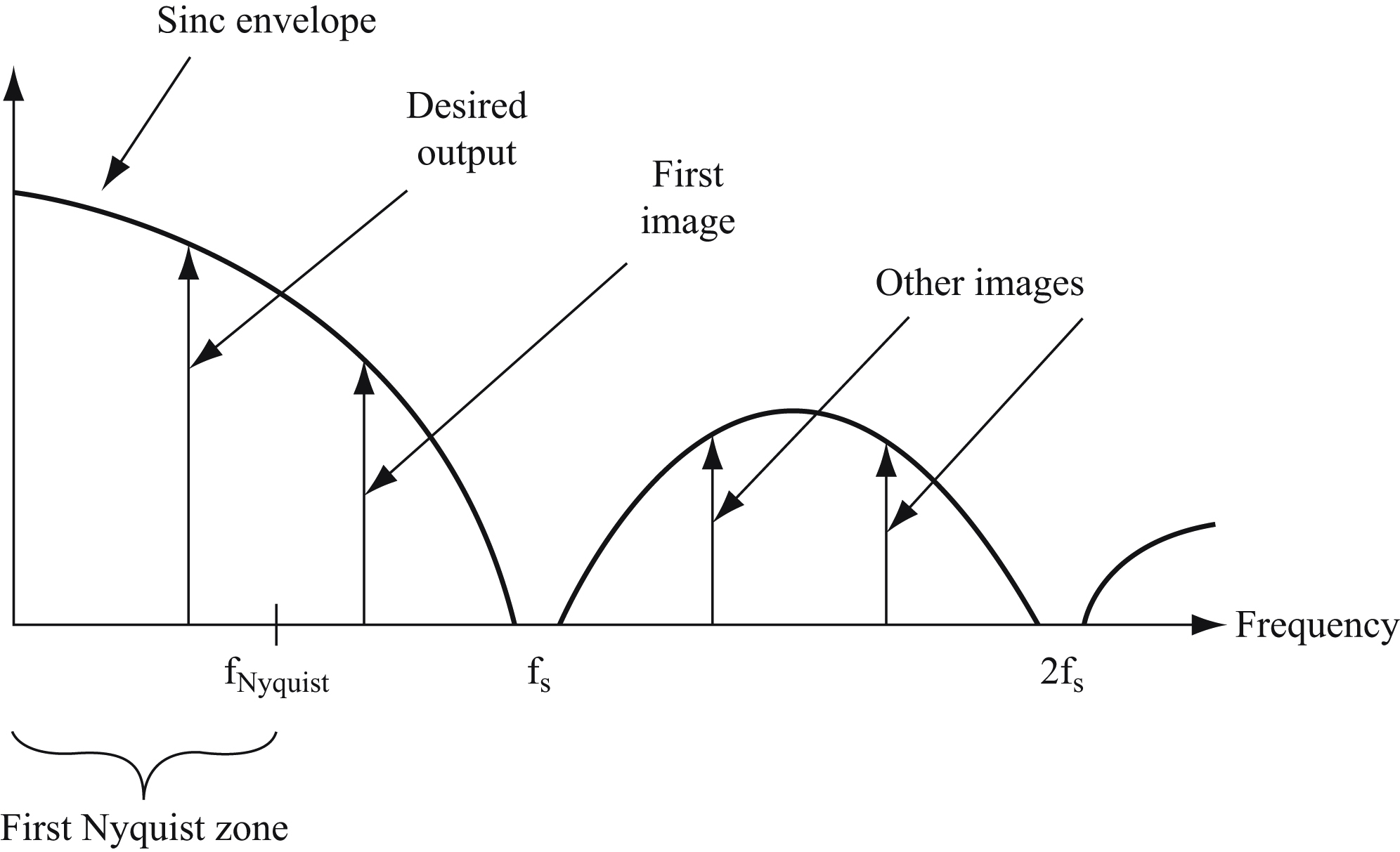
The sample and hold function is rectangular filter in the time domain. Each digital sample input is an impulse of a given magnitude. The output is a rectangular shape of the input magnitude. The DAC impulse response, just like in any filter, will define the frequency response. In this case, the rectangular impulse response yields a sinc function (sin(x)/x) response in the frequency domain. This is shown in the below, with the nulls in the frequency response corresponding to multiples of the DAC conversion or clock frequency (Fs) (Fig 11.9).
What this means in practice is that there will be a reduction in signal level at higher frequencies. By the time the DAC frequency response reaches the Nyquist frequency (½ Fs), it will have a droop of nearly 4 dB. The peak of the first lobe is 6 dB below the DC response, and second lobe peak a further 6 dB lower. Due to this attenuation, usefulness of the DAC output at frequencies well above the DAC Fs limited. Moreover, as the frequency response is not flat, it often needs to be compensated for. The closer the IF signal lies to multiples of the DAC Fs, the more distorted the frequency response is. Therefore, the IF frequency is usually limited the first Nyquist zone. Furthermore, it is usually limited to about 80% of the Nyquist frequency or to 40% of the DAC Fs. For a DAC being clocked at 250 MHz, the upconverted IF signal should be at 100 MHz or less. For example, if the IF carrier is chosen to be 70 MHz with complex baseband signal extending to 10 MHz, the IF signal will occupy a spectrum from 60 to 80 MHz. After the DAC, the analog output will need to be filtered using an analog filter to remove the higher frequency DAC images and the DAC clock harmonics. Often, a SAW (surface acoustic wave) bandpass filter is used, and the choice of IF frequency is often determined in part by the frequencies where the SAW filters are commercially available.
Many systems, particularly if the IF signals have fairly wide bandwidth (like our 4G wireless example with an IF signal BW of 20 MHz), will need to compensate for the frequency response droop due to the sinc response of the DAC even at these low IF frequencies. To do this, a sinc compensation FIR filter is used, after the NCO and complex multiplier performing the digital upconversion.
Below in Fig. 11.10 is the frequency response of a typical sinc compensation FIR filter, calculated using a popular digital signal processing design tool called Matlab (available from The Mathworks). It will compensate up to 80% of the Nyquist frequency. This digital filter would immediately preced the DAC and be placed after the digital upconversion process. It would have a data throughput rate equal to the DAC conversion rate. The associated coefficients are shown in Fig. 11.11.


..................Content has been hidden....................
You can't read the all page of ebook, please click here login for view all page.