
15
Manufacturing Processes in the Electronics Industry
15.1 Introduction
Almost every manufactured product we use today either contains electronic components, or has been designed and made by processes utilising electronics. The wordprocessor being used to write this sentence contains semiconductor based technology, the plastic for the keyboard was made by electronically controlled moulding processes and the assembly of the individual components was done by microprocessor‐controlled machines. Motor cars are designed using electronic computers, they are assembled using microprocessor‐controlled robots and often they contain such items as electronic ignition, instrumentation and fuel management systems. Our complex and varied telecommunication systems utilising land lines, microwaves and satellites would not operate without electronics. To supply this ubiquitous hardware we rely on the electronics manufacturing industry.
At the beginning of the twentieth century no electronics industry existed. Then in 1904 the thermionic valve was invented and this was followed in 1906 by the triode. These components made possible the construction of many of the electronic devices we know today, albeit in a relatively slow and cumbersome manner. For example, 40 years after the invention of the triode the electronic computer ENIAC required approximately 1400 m2 of floor space, weighed around 30 500 kg and contained 18 000 vacuum tubes. However, 1947 saw the invention of the transistor; this semiconductor technology was rapidly developed and by the 1960s many transistors, diodes, resistors and capacitors could be produced on the one ‘chip’ of silicon material; these were called integrated circuits (ICs). In 1970, an IC that could carry out many of the activities associated with computing was produced; this was the microprocessor. By the middle of the 1980s a million components could be created on a single chip, that is, very large scale integration or VLSI. Today, we have computers that can fit in our pockets whose power would amaze those who worked on ENIAC. At the time of writing there are chips with 15–30 billion transistors using 16, 14 and 10 nm (nanometre) technology. Difficulties arise with the commonly used silicon base as the transistor size approaches 7 nm. This is because as the 7 nm point is reached the electrons can begin to experience quantum tunnelling that normally occurs with barriers of around 3 nm and under. However, work is ongoing to achieve practical sub 7 nm sizes by using nanotechnology and materials other than silicon.
This chapter is concerned with the manufacturing processes used to produce semiconductor electronic components and the printed circuit boards (PCBs) on which they are assembled. The assembly process itself will also be briefly examined. Though not included here, other discrete components are found in electronic systems. For example, resistors may have a wound wire, conducting metal oxide film or carbon powder construction, and capacitors can be made from sheets of metal foil and insulating material wound into a compact canned package. Also to be found may be components such as potentiometers, switches and liquid crystal displays.
15.2 Semiconductor Component Manufacture
Semiconductor materials are so called because they have electrical properties that lie between those of conductors and insulators. However, what makes them useful is that their electrical properties can be altered by adding carefully controlled amounts of impurity atoms, called dopants, to their crystal structure. There are two types of dopant – the ‘n’ type that makes the material electron rich and the ‘p’ type that makes the material electron deficient. A component is constructed on a crystal of semiconductor material by selective doping. For example, by creating an n‐type element in contact with a p‐type element, a p–n junction is produced. This creates a diode junction since the configuration will conduct current only in one direction see Figure 15.1.
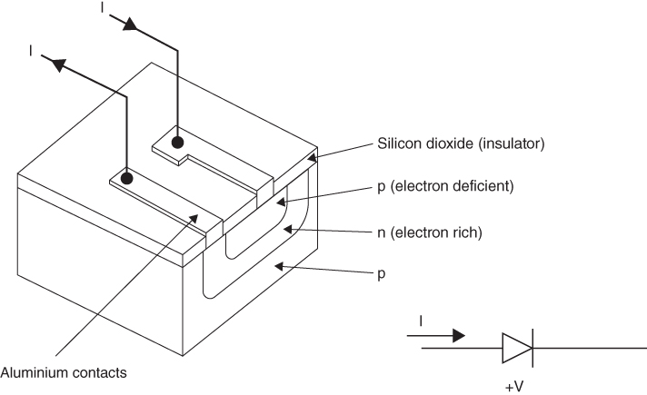
Figure 15.1 A semiconductor diode configuration.
Semiconductor components such as transistors and diodes can be manufactured as discrete items for use in a multitude of products such as radios and televisions. They are also used as discrete components in power handling applications where relatively large currents are being manipulated. However, although the basic technology is the same, the most complex conditions occur when large numbers of them are being created on a single chip, that is, the IC mentioned in the previous section. It is this situation, the manufacture of an IC chip, that is considered here.
The chip manufacturing process comprises a number of steps; these are shown in a very simplified form in Figure 15.2.

Figure 15.2 An integrated circuit manufacturing sequence.
15.2.1 Crystal Growing
The most widely used material for semiconductor component manufacture is monocrystalline silicon. This is because of its special atomic structure, its oxide (silicon dioxide) that is a very good insulator and can therefore be used for isolating components and component elements on a chip and its abundance in nature. Other materials used are cadmium sulfide for photo‐electric cells, lead sulfide for infrared sensors and gallium nitride for LEDs. Another more expensive material is gallium arsenide, ICs fabricated on gallium arsenide operate much faster than silicon based devices and they also have the ability to transmit light; this allows lasers and light emitting diodes to be constructed. However, the fact that the processing of gallium arsenide is relatively complex and that it is expensive means that silicon retains its popularity as a substrate material.
Silicon occurs in quartzite sand, that is, silicon dioxide. It must be purified before it becomes the flawless single crystal needed for chip manufacture. First it is heated with carbon, that is, coal or coke, in an electric arc furnace to produce polycrystalline silicon that is about 97% pure. It is then further processed by heating, fractional distillation as a chloride and vapour deposition to eventually produce polycrystalline silicon that is virtually 100% pure. This is now melted in a quartz crucible; dopant material may also be added at this stage. A seed crystal of silicon is dipped into the melt and then withdrawn very slowly while also being rotated. The melt material solidifies onto the seed crystal so forming a larger crystal, called a ‘boule’, which is eventually about 0.15 m diameter and 1 m long. This crystal growing is called the ‘Czochralski process’. The boule is then inspected for flaws, its electrical properties tested and defective parts removed. Since the crystal growing process does not allow tight control of the diameter size the boule is now turned and ground to produce a precise cylindrical shape between 50 and 150 mm in diameter and 1 m in length. It is then sliced into wafers about 0.5 mm thick using a diamond saw. These are polished to a mirror finish and inspected to ensure that any damage caused by the sawing process has been removed. Crystal growing and wafer production is carried out by companies specialising in this work. Therefore, the final stage is to pack the wafers and despatch them to the component manufacturer's factory.
15.2.2 Integrated Circuit Production
Although the following steps are the basic ones used in IC production, it should be remembered that the actual manufacturing process will involve repetitive implementation of these steps to produce a number of different levels, doped regions and electrical interconnections on the one chip.
15.2.2.1 Photolithography
None of the conventional machining processes are capable of producing the fine definition required to produce billions of transistors on, for example, a 400 mm2 chip of silicon. Resort has to be made to photographic techniques. Even here, visible light cannot be used as its wavelength, from about 0.4 μm to just under 0.8 μm, is too coarse for the definition required in these circuits. For this reason deep ultraviolet light lasers or electron beams with much smaller wavelengths are used to provide very fine resolution.
Photolithography involves printing patterns of the circuits and their elements onto a mask. Since each wafer of silicon is used to produce a large number of ICs the pattern is repeated many times on the one mask. The mask itself is produced photographically on glass from information produced by a CAD system. An image of the patterns is projected from the mask onto the wafer, which will have been previously coated with a photosensitive film. This film, called a photoresist, when exposed to ultraviolet light or electron beams becomes either more (‘positive resist’) or less (‘negative resist’) soluble to an etchant solution. Thus, after exposure the wafer can be treated with the etchant to leave the appropriate parts of its surface exposed. Layer fabrication can now take place, these exposed surfaces being subjected to processes such as oxidation, dopant diffusion, vapour deposition or further etching. The design of the IC will determine how often, and in what order, these processes are carried out. Between each step, the photolithography process will be used to produce new patterns.
15.2.2.2 Oxidation
As noted earlier, silicon dioxide is an excellent insulator; it also effectively blocks the dopant diffusion process, adheres strongly to the silicon substrate and is able to be removed by an etchant that does not attack the substrate. It is therefore used to create masks on the chip surface and to separate individual ICs on the wafer; it is also used as an integral part of the circuits and components themselves.
To create an oxide pattern on a silicon substrate the following procedure is carried out. In ‘dry oxidation’ the silicon substrate is exposed to an oxygen rich atmosphere in a furnace at a temperature of between 900 and 1200°C. This simple process causes oxidation of the silicon surface. When carried out in an atmosphere containing steam the process is called ‘wet oxidation’; this produces a higher oxide growth rate but with lower density. Thus a combination of both the dry and wet processes are often used. After cleaning, the oxide surface is coated in a photoresist material that is then pre‐baked in an oven at about 100°C. The photolithography process is now implemented as described earlier. Assuming that a positive resist has been used and the exposed resist has been removed by an etchant solution, the remaining resist is toughened by a post‐baking operation. This now allows the uncovered oxides to be removed down to the substrate level by another etchant, thus creating the desired pattern. Finally, the remaining photoresist is removed by dipping in a dissolving solution such as acetone.
15.2.2.3 Chemical Vapour Deposition and Dopant Diffusion
This is the process that is used to create the p‐ and n‐type semiconductor regions on a substrate. It is carried out by placing the substrate in an atmosphere of chemical vapours that deposit the dopant. The process is carried out in a furnace at a temperature between 800 and 1200°C. While in the furnace, atoms from the dopant material diffuse into the silicon substrate, thus causing displacement of the silicon atoms.
15.2.2.4 Metal Vapour Deposition
The devices produced by the foregoing processes all need to be interconnected by metal conductors to allow the IC to operate; vapour deposition is the process used to create these conductors. Normally aluminium or aluminium alloy is used, but for higher device densities tungsten may be necessary: again, photolithography and etching are used to create the connector paths. In vacuum deposition the wafer is placed in a vacuum where the metal to be deposited is melted. Under these vacuum conditions the metal boils and deposits itself on adjacent surfaces. The process is therefore so organised that the metal vapour, which propagates out from the melt in a straight line, coats the desired surfaces. Chemical vapour deposition is also used for depositing thin films of non‐metallic materials onto a substrate.
After all these processes have been carried out on the wafer a number of times and the ICs have been created, they have to be tested then separated. Testing is carried out automatically by needle probes contacting appropriate points on the circuits. Computer programs run the tests and flawed ICs are automatically marked with an ink dot. The ICs are then separated by either diamond sawing or scribing along lines between the ICs and snapping them off rather like tile cutting. At this stage in the process the ICs are usually called ‘dies’.
15.2.3 Packaging of Integrated Circuits
Since the individual dies are fragile and easily damaged they must be given a protective casing. They also need to be provided with connections of a practical size to enable them to be connected into circuits on PCBs and soon. The die may be attached to its protective casing or package by metallising the back then soldering it onto a metal plate in the package, or it may simply be epoxied into place. The package will have metal leads to allow connection to the outside world. The die will have metallised contact pads created by the vapour deposition process mentioned earlier. These contact pads are connected to the package leads by pressure or ultrasonic bonding techniques. The package is then closed and sealed while ensuring that no moisture or contaminants are included, see Figure 15.3.

Figure 15.3 An integrated circuit in a dual in‐line package.
The package is now given its final tests. Those that must exhibit very high reliability, for example, for aerospace and military use, are given high temperature, temperature cycling, vibration and other tests to ensure that the circuits that would fail early in their service life are identified.
15.3 Clean Rooms
With component dimensions in ICs being much less than 1 μm in size it is apparent that contamination by foreign particles during manufacture could be a serious problem. For example, human hair is between 30 and 100 μm in diameter, bacteria between 0.3 and 30 μm, and tobacco smoke between 0.01 and 1 μm. To avoid contamination by foreign particles special rooms are built for semiconductor manufacture and other fine assembly work; these are called ‘clean rooms’, and incorporate a number of techniques for ensuring a clean environment.
To prevent contaminated air entering the room, air has to pass through high efficiency filters; these must be almost 100% efficient at removing particles which under the most stringent conditions would be less than 0.1 μm. Charcoal filters may also be used to remove chemical contaminants from the air. To make sure that only cleaned air is present in the room a positive air pressure differential is created between the room and the outside factory. This pressurisation ensures that air will only escape from the room and outside air can enter only through the filtering system.
Although air into the clean room can be filtered, humans inside the clean room present a major source of contaminants. Although eating, drinking and smoking are prohibited, humans still constantly introduce contaminants from breathing, skin particles, hair and clothing. To eliminate this contamination surgical masks, gloves, hair caps and gowns are worn by operators. For ultra clean rooms, the workers may be completely isolated from the environment by wearing one‐piece overalls and visored helmets that drape over the shoulders and are connected by tube to an external air supply. A differential air pressure is again created between the inside of the suit and the clean room to ensure that air travels from the room into the suit and not vice versa. Airlocks are used by the personnel when moving in or out of the clean room.
Clean rooms are classified by a number that indicates the number and size of particles that are permitted per m3 in ISO (International Organisation for Standardisation) standards or per ft3 in US Federal standards. Ambient city air can contain 35 000 000 particles of 5 μm and larger per m3. In extreme cases clean rooms can provide atmospheres containing less than 12 particles of 0.3 μm m−3 although most clean rooms will be considerably less stringent than this.
15.4 Printed Circuit Board Manufacture
The individual ICs are seldom used on their own in electronic products. Usually discrete components with operating characteristics that prevent their miniaturisation are also required: for example, components that cannot be integrated such as inductors, large resistors that require extra heat dissipation, large capacitors, power transistors, potentiometers, mechanical switches and other ICs. A means of holding all of these components that will allow them to be connected to each other and to the outside world is necessary. This means is usually provided by a printed circuit board – often abbreviated to PCB. A block diagram of the steps involved in PCB manufacture is shown in Figure 15.4.
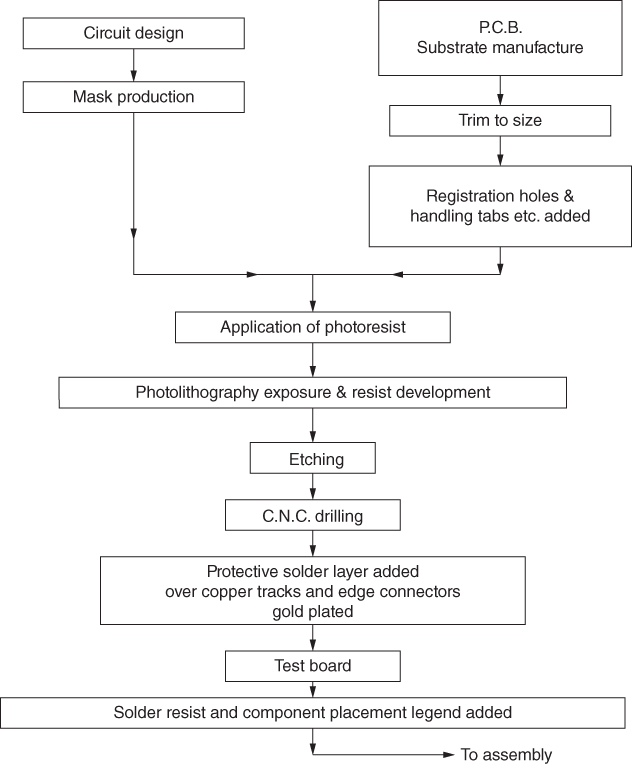
Figure 15.4 Single‐sided PCB manufacturing sequence.
PCBs are available in a variety of types and complexities. They are usually rigid, though some are flexible, and they are made from a paper or glass reinforced plastic resin coated with a copper foil. The conductive tracks on the surface of the board are created by screen printing or photolithography and etching. The boards may be single sided, that is, conductive tracks on only one side or double sided. Multi‐layered boards are also used. These are equivalent to a number of single or double sided PCBs made into a sandwich, each layer being separated by glass reinforced plastic and interconnected by conductive ‘via’ holes.
- Substrate manufacture. The board substrate is made under clean room conditions since any contaminants on the copper surfaces could prevent proper functioning of the board in service. For single‐ and double‐sided boards the copper foil, usually produced by electroplating, is placed on the highly polished surface of a steel plate resting in a press. Assuming that a glass reinforced plastic substrate is being created, layers of glass cloth impregnated with an epoxy resin are placed in layers on top of the copper foil until the desired thickness is obtained. Finally, either a release film is added for single sided boards or another sheet of copper foil for double sided boards. Another highly polished steel plate is attached to the press ram. By using high pressures and steam heating of the steel plates the boards are compressed and the resin cured. After cooling, the boards are trimmed to remove excess resin. Usually one press has many plates and can therefore produce many boards at each pressing. Boards are usually produced in standard sizes to allow them to be easily used with automated equipment at later stages. For simplicity, the following stages refer to single sided board manufacture.
- Pre‐processing. At this stage the boards are prepared for processing by adding certain features. Registration holes have to be created to assist with board location in subsequent processes; these will enable, for example, the board to be located properly while component holes are drilled automatically at appropriate positions on the tracks. Handling tabs may also be added by stamping to facilitate later automated handling. The board may also be given a unique identification at this stage by adding a bar code or alphanumeric characters. The board is then thoroughly cleaned before passing to the next stages.
- Photolithography. This process is very similar to that described earlier for IC manufacture. In this case, the photoresist is usually added in the form of a photosensitive polymer. The polymer is held between two dry cover films and supplied in rolls. By removing one of the films the polymer can be applied directly to the board surface. The second film may be removed at this stage or kept in place until later. The board is now exposed to ultraviolet light projected through a mask containing an image of the required track layout. It is then developed by chemical removal of the exposed resist, usually by using a solvent.
- Etching. The exposed copper surfaces can now be removed by etching with a solution such as ferric chloride or copper chloride and hydrochloric acid. This is usually done by spraying the board with the etchant, as this provides greater control than total immersion. After all the exposed copper has been etched away, the remaining resist material is removed. This produces the desired copper tracks on the PCB surface.
- Drilling. This is carried out to create the holes for component leads and pins, and also for bolting and screwing holes to take larger components such as transformers and heat sinks. The precision with which these drill holes are located is extremely important since automated component insertion methods may be used. A number of boards may be drilled at the same time by creating a stack and drilling through. The drilling will probably be carried out by a CNC, that is, a computer controlled drilling machine. These machines will automatically drill the required pattern of holes based on instructions received from the CAD system used to design the board layout. Drilling is also used to create the ‘via’ holes in double sided and multi‐layer boards. The boards are passed between abrasive rollers to remove the rough edges created around the drilled holes; this is referred to as deburring.
- Board finishing. The board now has bare copper tracks and ‘lands’ (these are the local areas where the track is widened around the lead holes or surface mounted device (SMD) contact points). To prevent the copper oxidising, which would give problems later at component assembly, it is given a coating of solder. This is done by plating or a process known as roller tinning. Edge connectors are usually gold plated for reliability. The board is then tested for continuity of the tracks and inspected for flaws. Finally, the component locations are identified by means of a printed legend and, with the exception of the lands, the board is coated in solder resist.
15.4.1 Assembling Components to Printed Circuit Boards
Having considered electronic component and PCB manufacture, we will now examine how they are assembled together to produce a finished ‘populated’ PCB. Component configuration and presentation are considered before looking at the final assembly process.
15.4.1.1 Component Configurations
Electronic components can be classified as: (i) leaded, these may have axial, radial, or dual in line (DIP) leads; (ii) surface mounted, these have no leads and (iii) non‐standard. Sketches of these configurations are shown in Figure 15.5. Non‐standard components may be edge connectors, switches, transformers and so on. Discrete resistors often have an axial lead configuration, transistors have a radial and ICs a DIP. Components produced in leaded configurations can also be produced as surface mounted devices; that is, SMDs. In comparison to leaded components. SMDs allow the production of more densely populated boards, that is boards can be made smaller yet perform the same functions; they have a physical construction ideally suited to automated PCB manufacture, they can be mounted on both sides of the PCB and therefore the only holes needed to be drilled in the board are ‘via’ holes for electrical connections between each side. However, they may be more expensive than the leaded type and difficult to assemble manually. Because of this and difficulties in making some leaded components in SMD form, PCBs are usually populated by a mixture of leaded, SMD and non‐standard components.

Figure 15.5 Component configurations.
Axial and radial leaded components are usually packaged in edge tape bandoliers or sprocket feedable tapes, DIPs in linear stick magazines and SMDs in blister tapes or stick tubes. These are shown in Figure 15.6. In some systems, many bandoliers, each carrying one type of component, are used automatically to create a new bandolier that will have all components sequenced in the correct order for automatic assembly in a special component insertion machine. DIPs can be provided in magazine packages. These can be mounted at the workstation in such a manner as to allow the DIPs to slide out of the magazine onto a rail where they can easily be picked up manually or automatically for assembly. For SMDs, stick tubes are similarly used, or by peeling off a retaining tape, blister packages can be fed past the component pick up points at an assembly station.
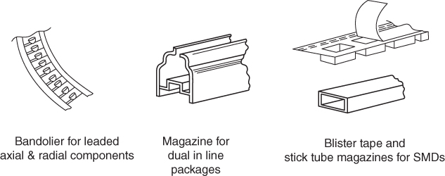
Figure 15.6 Component delivery packages.
15.4.1.2 Assembly Methods for Leaded Components
Electronic components are assembled to PCBs manually, automatically or by a combination of manual and automatic methods.
Manual assembly methods are used for shorter production runs, where relatively slow production rates of up to say 500 components per hour are to be placed or where the components are difficult to assemble by other means. Leaded components need to have their leads cut to length and pre‐formed before insertion, see Figure 15.7a. In manual assembly this can be done by the operator using pliers or by using a special die (in automatic assembly the pre‐forming is done automatically using special tooling). The operator lifts the component from a bin or presentation point and places it into the CNC drilled holes in the PCB. These holes will have been marked at the PCB manufacturing stage with identification numbers to assist the operator. A further refinement is to use a machine that presents the components to the operator in a specific sequence; this is synchronised with a projector placed over the board. The projector is supplied with a roll of film that is indexed to allow the position of each component to be illuminated on the board as the operator carries out the insertion. For very small volumes the assembled PCB may have each component individually hand soldered, but it is more likely that the board will move on to an automated soldering process such as wave soldering.

Figure 15.7 (a) Preformed axial and radial leads and (b) SMD onsertion using adhesive.
Automated assembly is used for higher volume production. Typically industrial robots will be used where the demand is for around 1800 components per hour to be assembled, since robots can be easily reprogrammed to cope with changing production requirements. For higher production rates, say up to 30 000 per hour, dedicated automated assembly machines are used. Axial and radial leaded components are automatically removed from their bandoliers or sprocket feedable tapes, their leads are preformed, they are inserted and then their leads are cropped and clinched ready for soldering. DIPs are gravity fed from their stick magazines to their appropriate pickup points.
After insertion the components must be soldered to provide the electrical connections between them and the PCB land areas (lands are the wider parts of the PCB tracks around the component holes). This operation requires the application of a flux to remove metal oxides and contaminants and to distribute the applied heat uniformly across the joint, and a molten solder. For large volumes, production techniques such as wave soldering are used. Here the boards are mounted on conveyor tracks which support them along two edges. The boards then have flux applied to them by one of three methods. They may pass through a bath of flux foam, over a wave of flux created in a bath or they may be sprayed with flux. They then pass through a pre‐heating operation that raises their temperature to about 90°C and activates the flux. The board then passes over the surface of a bath of molten solder. A wave of solder is created in the bath as the board passes such that all exposed conducting surfaces are coated in solder.
15.4.1.3 Assembly Methods for SMDs
Since surface mounted devices have no leads, different techniques for holding them in position on the PCB and soldering are needed. Two main methods are used, the first being adhesive and wave soldering. In this method adhesive is applied to the PCB at appropriate points see Figure 15.7 b. The adhesive can be applied by a screen printing process or by dispensing from a syringe. The SMD is then placed onto the board, probably using an automated pick and place unit in such a manner as to ensure it is making contact with the PCB lands and the adhesive coated areas. The adhesives used are curable and depending on type the adhesive is now cured by exposing it to ultraviolet light or heat. The components are finally soldered to the board using the flow solder process. This differs from the soldering of the leaded components in that the SMDs themselves have to pass through the solder wave, therefore particular care has to be taken to ensure proper adhesion of the components before soldering begins.
The second method is called the solder paste and reflow solder method. In this, the solder paste acts as both the adhesive and the conductor. The paste is actually a suspension of powdered solder particles in a flux. Just as in the previous technique the paste is applied by either screen printing or syringe. The SMDs are then inserted by automatic pick and place devices. It is apparent that one of the qualities of the solder paste must be that it has a high enough viscosity to ensure that components stay in their positions throughout the process. The boards are then passed through the reflow stage in which the solder is melted and cooled to form the finished conductive joint. Various methods of melting the solder are used, two of which are the infrared and vapour phase. In infrared reflow soldering, the boards are carried on a conveyor past a series of infrared lamps or heaters. It is relatively inexpensive and can handle high quantities, but consistent quality is more difficult to maintain. In the vapour phase method a suitable inert liquid is heated and vaporised in a tank. The PCBs are then placed in the tank where the vapour condenses onto their surfaces. During condensation the latent heat of the vapour is transferred to the solder, causing it to melt. The process can be made continuous by passing the boards through the tank on a conveyor. This method produces good quality joints, but is relatively expensive and slow.
15.5 Conclusion
The manufacture of electronic components and assemblies includes a wide variety of processes that require inputs from many different disciplines in science and engineering. The chapter is intended to provide only an indication of the depth of the subject. For example, one area not covered has been that of testing. Completed assemblies require to be tested in a variety of ways, for example, the operation of the individual components, the continuity of the electric circuit, the positioning and polarity of the components, and the functional performance of the complete assembly are all factors to be considered. Special test rigs, artificial vision systems and chambers where the boards can be subjected to thermal cycling, high humidity conditions, vibration and so on are all used to ensure that products are up to the high quality demanded by international markets.
Review Questions
- 1 Discuss the significance of the invention of semiconductor technology.
- 2 What is an IC chip? Sketch a block diagram of the steps involved in its manufacture.
- 3 Briefly outline the Czochralski process.
- 4 Describe the process of photolithography and discuss its use in the electronics industry.
- 5 Why is silicon dioxide an important material in IC manufacture; how is it obtained?
- 6 Briefly describe the processes of dopant diffusion and vapour deposition, and their use in IC manufacture.
- 7 Discuss why clean rooms are necessary in IC manufacture.
- 8 By the use of a block diagram, briefly outline the steps involved in the manufacture of printed circuit boards (PCBs).
- 9 Describe the differences between leaded components and SMDs, and discuss why the latter are increasing in popularity.
- 10 Briefly outline the operations involved in PCB assembly.
- 11 Describe the processes of ‘adhesive and wave soldering’ and ‘solder paste and reflow soldering’, and state where they are used.