
1.2
How Lithography Enables Moore's Law
J. P. H. Benschop
ASML, Veldhoven, The Netherlands
1 Introduction
Over the last 50 years, Moore's Law has set the pace for the electronics industry, delivering increasing computing capabilities at stable cost. This was driven by the steady pace of the increase of components in an integrated circuit (IC), which has to a large extent been enabled by optical lithography printing increasingly smaller electronic features on a silicon wafer.
We will quantify what the contribution of lithography to Moore's Law has been in the past and then discuss the future lithography options to extend Moore's Law into the future.
2 Moore's Law and the contribution of lithography
In 1965, Moore observed that the number of components in an IC or (micro)chip, doubled every year1 and he predicted this would continue. Due to the high fixed costs to produce a single chip, increasing density would lead to lower cost per component. This empirical observation of economics became later known as “Moore's Law.”
In a later paper, Moore quantified the contributions to a doubling of components per year2: die size reduction (∼30%), dimension reduction (∼30%), and “device and circuit cleverness” (∼40%). Lithography, enabling the dimension reduction, thus contributed to a doubling of components per chip every 3.3 years. In that same paper Moore predicted that the components per chip would double every 2 years, compared with his previous prediction of 1 year. This revised “shrink” rate has since continued and has set the pace for the semiconductor industry over the past 40 years.
In a 1995 paper3 by Moore, the contribution of lithography to the increased density was shown. From this graph, it can be concluded that lithography leads to a doubling of components per square centimeter every 2.8 years. Hence the contribution of lithography to Moore's Law has been fairly constant from the beginning, see Fig. 1.
Table 1 The evolution of wavelength, NA and k1 over the years
| David Mann (GCA) 4800 | ASML/40 | ASML/300 | ASML/1100 | ASML 19×0i | ASML 3100 | ASML 3300 | |
| Year of 1st prototype | 1975 | 1987 | 1995 | 2000 | 2007 | 2009 | 2012 |
| Wavelength (nm) | 436 | 365 | 248 | 193 | 193 | 13.5 | 13.5 |
| NA | 0.28 | 0.4 | 0.57 | 0.75 | 1.35 | 0.25 | 0.33 |
| k1 | 0.90 | 0.77 | 0.57 | 0.39 | 0.27 | 0.50 | 0.44 |
| CD (nm) | 1400 | 700 | 250 | 100 | 38 | 27 | 18 |
| Step/scan field (mm) | 10 × 10 | 14 × 14 | 22 × 27 | 26 × 33 | 26 × 33 | 26 × 33 | 26 × 33 |
| Pixels per field | 50 × 106 | 400 × 106 | 10 × 109 | 86 × 109 | 600 × 109 | 1.2 × 10¹² | 2.6 × 10¹² |
| Weight (kg) | 2 | 20 | 250 | 400 | 1080 | 700 | 1600 |

Figure 1 Contribution of lithography to Moore's Law: (a) 1960–1975 “dimensional reduction” doubles component density every 3.3 years; (b) 1970–1995 “minimum dimension” doubles component density every 2.8 years.
3 Lithography technology: past and present
Optical lithography has always been the workhorse for integrated circuit manufacturing. Since the late 1970s, optical projection has been used where a mask (containing the pattern to be printed) is demagnified and repeatedly imaged on a silicon wafer.
The resolution of the optical lithography tool is usually expressed by
where R is the half pitch, k1 is a process factor, λ0 is the wavelength in vacuum, and NA is the numerical aperture, given by the product of the refractive index n and sin(α) where α is the opening angle: ![]() . Note that the minimum k1 for a single exposure equals 0.25. This corresponds to two plane waves interfering from opposite sites, as illustrated in Fig. 2.
. Note that the minimum k1 for a single exposure equals 0.25. This corresponds to two plane waves interfering from opposite sites, as illustrated in Fig. 2.

Figure 2 Resolution is defined as the half pitch of a dense pattern of repeated lines and spaces. Minimum resolution R, resulting from two waves interfering from the opposite sides is given by 0.25λ0/NA.
To improve the resolution, and thus enable Moore's Law, all three parameters in Eq. (1) have been improved over time. Thus, for the process factor k1 the main developments have been as follows:
- Pushing the single exposure as close as possible to physical limit of 0.25 using image enhancement4 (e.g., source mask optimization5) and feedback loops (metrology to measure printed patterns feeding back to many actuators in the lithography tool, such as focus, dose, and illuminator mode,6 bring IC printing closer to the physical limit);
- Frequency doubling by multiple exposure7 or spacer technologies8 that enable a k1 < 0.25.9
Progress in the wavelength and numerical aperture parameters is summarized in Table 1. We observe that over the years the wavelength λ0 has decreased from 436 nm (g-line of mercury) to 365 nm (i-line of mercury) to 248 nm (KrF laser) to 193 nm (ArF laser). It also shows that the NA was increased from 0.28 to 1.35 (using a water-based “immersion”-extension of the lens to replace the air between the lens and the wafer). The most recent step to extreme ultraviolet (EUV) wavelength (EUV of 13.5 nm using a plasma source) is so significant (15× improvement) that the NA could be relaxed to 0.33 from 1.35.
Table 1 shows how decreases in wavelength and improvements in NA, in combination with a decrease in k1, have led to an increase of the pixels per field by a factor of over 105 over the last decades.
4 Lithography technology: future
Here we review the leading lithography candidates to extend Moore's Law.
• Multiple patterning immersion lithography
There is no fundamental limit to frequency multiplication. Octuple patterning has resulted in 5.5 nm lines,10 35× smaller than the wavelength of the light used to print the pattern. There are, however, practical limitations:11 increased process complexity leads to increased cost and cycle time and there is the overlay/edge placement challenge.12
• Directed self-assembly
Block copolymers are two different types of polymer chains (e.g., PS and PMMA) connected at one end. The polymer blocks phase-separate as a result of the chemical differences between the polymers and self-assemble in regular patterns at the molecular scale, see Fig. 3. The size (from a few to tens of nanometer) and shape (cylinders, lamellae, etc.) depend on the molecular weight and composition of the copolymer.

Figure 3 Principle and practical results for directed self-assembly (DSA). (a) Ordered state energetically more favorable; (b) SEM picture of contact holes created by ArFi before (left) and after (right) DSA.
Lithography or any other top-down prepatterning technique is needed to induce a long-range ordering.13–15 Directed self-assembly (DSA) should therefore be seen as a technology complimentary to optical lithography. It enables a smaller feature size16 and/or better line edge roughness. It has been demonstrated that a 71–83 nm diameter contact hole printed with immersion lithography can be shrunk to a 29 nm diameter hole while reducing the three-sigma uniformity of the hole diameter from 3.5 nm (immersion) to 1.3 nm (DSA).17
The critical issues with DSA are defect density18 (compared to immersion lithography standard of tens per square centimeter) and placement error17 (which adds ∼2 nm additional error).
• Electron beam
Electron beam lithography offers excellent resolution but at very low productivity. It has been used for many years to write the masks used in optical lithography.
Multiple direct write e-beam lithography concepts are being pursued. In order to increase productivity, various concepts, leading to many beams used in parallel, are being pursued – see Fig. 4 for progress in recent years. These include the following:
- MAPPER,19 a 5 kV raster wafer writer with a single source, multiple lenses (target 13,000), and multiple spots per lens (49 realized);
- IMS,20 50 kV raster mask writer, single source, many spots (262,144 realized) in single lens field;
- multibeam21 wafer writer, vector scan, multiple column, one beam per column.
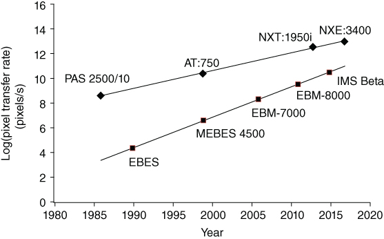
Figure 4 Pixel transfer rate of optical and e-beam lithography tools over the years.
These concepts each have their own pros and cons. However, a critical factor for any e-beam system is the extendibility. Next to the fact that shot noise will mandate an increased dose to reach smaller resolution (a factor e-beam has in common with optical photon-based lithography), electron–electron interaction makes it extremely difficult, if not impossible, to maintain productivity for smaller resolutions. Without concept changes, the estimated productivity decrease can be as large as a factor eight per node.22
• Imprint
The “step and flash” imprint technology is being pursued for use in IC lithography.
A master template is written with e-beam, inspected, and repaired. Imprint is used to replicate this master; the replica templates are used to imprint a wafer.23
The 1X mask is inherently difficult to write, inspect, and repair. The fact that it is repeatedly used in contact with the wafer makes lifetime a critical issue.
Another critical issue is overlay. In particular, mix and match to optical systems is more difficult since deforming the mask has limited correction capability compared to the many parameters officered in an optical lens.
Despite significant progress over the recent years,24 the achievable numbers for defect density, contamination, and overlay need significant improvement before this technology can be used in volume IC production (see Table 2 in Section 5).
Table 2 Comparison of state-of-the-art lithography results as of the time of writing
| ArFi25 | EUVL26 | DSA17 18 | e-Beam19 27 | Imprint23 | |
| Resolution | 38 nm L/S 19 nm SADP 10 nm SAQP |
13 nm L/S at 0.33NA 9 nm SADP |
14 nm L/S with PS-PMMA <10 nm L/S with high chi materials |
16 nm L/S trade-offs in dose and throughput | Can reproduce e-beam resolution: <15 nm L/S |
| Overlay (mixed machine) | <2.3 nm Mixed machines |
<2 nm Single machine |
2 nm added to ArFi overlay (RSS) | 10 nm | 4.8 nm Single machine |
| Throughput | >250 wafers/hour | Current: ∼55 wafers/hour at 80 W Target: 125 wafers/hour at 250 W |
∼150 wafers/hour track process with 5 min anneal time | 1 wafers/hour 10 wafers/hour with 49 × 13 K beams |
10 wafers/hour Per station |
| Defect density | <1 cm−2 | <1 cm−2 mask <1 cm−2 wafer |
24 cm−2 | <1 cm−2 mask | 9 cm−2 |
• Extreme ultraviolet (EUV)
EUV lithography uses 13.5 nm light and multilayer reflective optics. It has been intensively pursued since the 1980s, as illustrated in Fig. 5.28–30

Figure 5 History of EUV lithography.
(Source: Courtesy of ASML).
Over the last decade, several generations of full-field EUV scanners have been shipped.31–33 The latest NA = 0.33 EUV scanner has demonstrated excellent imaging and overlay,26 see Fig. 6. Throughput of 1000 wafers/day has been reached using an 80 W source. Yet consistently high productivity remains a critical issue. Availability needs further improvement, followed by a 4× increase in source power.
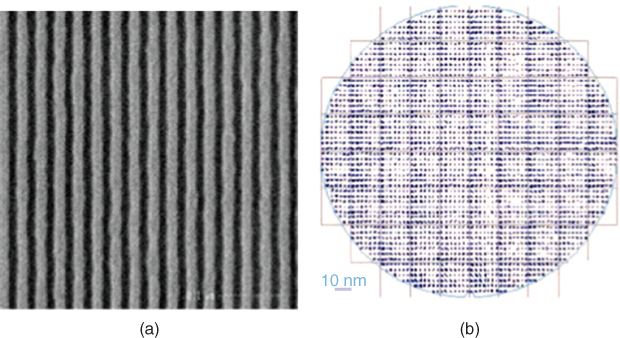
Figure 6 State-of-the-art imaging and overlay results: 13 nm dense lines and spaces (a); <2 nm overlay μ + 3σ in a single EUV tool (b).
Once EUV is inserted into high-volume manufacturing, it will extend Moore's Law by resolution-enhancing techniques34 (lower k1) and by introducing high NA.35
Another wavelength reduction to ∼6 nm has been explored and proof-of-principle of source36 and coatings37 have been demonstrated. Any wavelength change comes with significant challenges to the tool, as well as to the mask and resist infrastructures, and therefore it is not expected to happen anytime soon.
5 Summary
Status of today's and potential future lithography solutions is summarized in Table 2.
6 Conclusion
Optical lithography has enabled Moore's Law to continue for the last 50 years by a combination of wavelength decrease, numerical aperture increase, and process improvements (k1 factor decrease).
Optical lithography has been extended over the last decade by immersion lithography and multiple patterning. As such, it is today's workhorse for the semiconductor industry.
The next step for optical lithography is EUV, which will greatly simplify patterning and thus promises faster yield ramp and lower cost. It has far more industry support than alternative patterning techniques and is the leading candidate to succeed immersion lithography. Significant progress in EUV lithography has been made, yet sources need further improvement, as well as the tool availability.
As for the alternative patterning techniques, DSA still needs optical lithography to guide the patterns and should thus be seen as a complementary technology; e-beam is the technology of choice for mask writing but lacks the speed to compete in high-volume wafer patterning, whereas imprint is unlikely to overcome the challenges inherent to a 1X contact mask.
Acknowledgments
To all lithographers worldwide whose innovations enabled Moore's Law.
References
- 1. G. E. Moore, “Cramming more components onto integrated circuits,” Electronics 38(8), 114–117 (1965).
- 2. G. E. Moore, “Progress in digital integrated electronics,” Tech. Dig. IEDM (1975), pp. 11–13.
- 3. G. E. Moore, “Lithography and the future of Moore's Law,” Proc. SPIE 2438, 2–17 (1995).
- 4. J. Finders, M. Eurlings, K. V. I. Schenau, M. Dusa, and P. Jenkins, “Low-k1 imaging: How low can we go?,” Proc. SPIE 4226, 1–15 (2000).
- 5. R. Socha, X. Shi, and D. LeHoty, “Simultaneous source mask optimization (SMO),” Proc. SPIE 5853, 180–193 (2005).
- 6. J. Mulkens, P. Hinnen, M. Kubis, A. Padiy, and J. Benschop, “Holistic optimization architecture enabling sub-14-nm projection lithography,” J. Micro/Nanolith. MEMS MOEMS 13, 011006 (2014).
- 7. M. Dusa, J. Quaedackers, O. F. A. Larsen, et al., “Pitch doubling through dual patterning lithography challenges in integration and litho budgets,” Proc. SPIE 6520, 65200G (2007).
- 8. W.-Y. Jung, C.-D. Kim, J.-D. Eom, et al., “Patterning with spacer for expanding the resolution limit of current lithography tool,” Proc. SPIE 6156, 61561J (2006).
- 9. G. Capetti, P. Cantu, E. Galassini, et al., “Sub k1 = 0.25 lithography with double patterning technique for 45 nm technology node flash memory devices at λ = 193 nm,” Proc. SPIE 6520, article no. 011006 (2007).
- 10. K. Oyama, S. Yamauchi, S. Natori, A. Hara, M. Yamato, and H. Yaegashi, “Robust complementary technique with multiple-patterning for sub-10 nm node device,” Proc. SPIE 9051, 90510V (2014).
- 11. W. Arnold, M. Dusa, and J. Finders, “Manufacturing challenges in double patterning lithography,” IEEE Intern. Symp. Semicond. Manufacturing (ISSM-2006), paper MC-233.
- 12. J. Mulkens, M. Hanna, H. Wei, V. Vaenkatesan, H. Megens, and D. Slotboom, “Overlay and edge placement control strategies for the 7-nm node using EUV and ArF lithography,” Proc. SPIE 9422, 94221Q (2015).
- 13. M. P. Stoykovich and P. F. Nealey, “Block copolymers and conventional lithography,” Mater. Today 9, 20–29 (2006).
- 14. C. T. Black, “Polymer self-assembly as a novel extension to optical lithography,” ACS Nano 1, 147–150 (2007).
- 15. I. Bita, J. K. W. Yang, S. J. Yeon, C. A. Ross, E. L. Thomas, and K. K. Berggren, “Graphoepitaxy of self-assembled block copolymers on 2D periodic patterned templates,” Science 321, 939–943 (2008).
- 16. R. Ruiz, H. Kang, F. A. Detcheverry, et al., “Density multiplication and improved lithography by directed block copolymer assembly,” Science 321, 936–939 (2008).
- 17. S. F. Wuister, D. Ambesi, T. S. Druzhinina, et al., “Fundamental study of placement errors in directed self-assembly,” J. Micro/Nanolith. MEMS MOEMS 13, 033005 (2014).
- 18. H. Pathangi, B. T. Chan, H. Bayana, et al., “Defect mitigation and root cause studies in 14 nm half-pitch chemoepitaxy directed self-assembly LiNe flow,” J. Micro/Nanolith. MEMS MOEMS 14, 031204 (2015).
- 19. G. de Boer, M. P. Dansberg, R. Jager, et al., “MAPPER: Progress towards a high volume manufacturing system,” Proc. SPIE 8680, 86800O (2013).
- 20. E. Platzgummer, E. Klein, and H. Loeschner, “Electron multi-beam technology for mask and wafer writing at 0.1 nm address grid,” Proc. SPIE 8680, 868001 (2013).
- 21. D. Lam, D. Liu, and T. Prescop, “E-beam direct write (EBDW) as complementary lithography,” Proc. SPIE 7823, 78231C (2010).
- 22. M. Wieland, “Progress towards a manufacturing system,” Presented at Lithography Workshop (2015), available at www.lithoworkshop.org/2015-Lithography-Workshop-Program-Book-v1-2.pdf.
- 23. H. Takeishi and S. V. Sreenivasan, “Nanoimprint system development and status for high volume semiconductor manufacturing,” Proc. SPIE 9423, 94230C (2015).
- 24. K. Ichimura, K. Yoshida, S. Harada, T. Nagai, M. Kurihara, and N. Hayashi, “HVM readiness of nanoimprint lithography templates: Defects, CD, and overlay,” Proc. SPIE 9423, 94230D (2015).
- 25. S. Weichselbaum, F. Bornebroek, T. De Kort, et al., “Immersion and dry scanner extensions for sub-10 nm production nodes,” Proc. SPIE 9426, 942616 (2015).
- 26. A. Pirati, R. Peeters, D. Smith, et al., “Performance overview and outlook of EUV lithography systems,” Proc. SPIE 9422, 94221P (2015).
- 27. I. Servin, N. A. Thiam, P. Pimenta-Barros, et al., “Ready for multi-beam exposure at 5 kV on MAPPER tool: Lithographic and process integration performances of advanced resists/stack,” Proc. SPIE 9423, 94231C (2015).
- 28. H. Kinoshita, T. Kaneko, H. Takei, N. Takeuchi, and S. Ishihara, “Study on X-ray reduction projection lithography,” Presented at 47th Autumn Meeting Japan Soc. Appl. Phys. (1986), paper no. 28-ZF-15.
- 29. W. T. Silfvast and O. R. Wood II “Tenth micron lithography with a 10 Hz 37.2 nm sodium laser,” Microelectron. Eng. 8, 3–11 (1988).
- 30. A. M. Hawryluk and L. G. Seppala, “Soft X-ray projection lithography using an X-ray reduction camera,” J. Vac. Sci. Technol. B 6, 2162–2166 (1988).
- 31. H. Meiling, H. Meijer, V. Y. Banine, et al., “First performance results of the ASML alpha demo tool,” Proc. SPIE 6151, 651508 (2006).
- 32. C. Wagner, J. Bacelar, N. Harned, et al., “EUV lithography at chipmakers has started: Performance validation of ASML's NXE:3100,” Proc. SPIE 7969, 79691F (2011).
- 33. R. Peeters, S. Lok, J. Mallman, et al., “EUV lithography: NXE platform performance overview,” Proc. SPIE 9048, 90481J (2014).
- 34. S. Hsu, R. Howell, J. Jia, et al., “EUV resolution enhancement techniques (RETs) for k1 = 0.4 and below,” Proc. SPIE 9422, 94221I (2015).
- 35. B. Kneer, S. Migura, W. Kaiser, J. T. Neumann, and J. Van Schoot, “EUV lithography optics for sub 9 nm resolution,” Proc. SPIE 9422, 94221G (2015).
- 36. K. Koshelev, V. Krivtsun, R. Gayasov, et al., “Experimental study of laser produced gadolinium plasma emitting at 6.7 nm,” Presented at Intern. Workshop EUV Sources, Dublin, Ireland (2010).
- 37. T. Tsarfati, R. W. E. van de Kruijs, E. Zoethout, E. Louis, and F. Bijkerk, “Reflective multilayer optics for 6.7 nm wavelength radiation sources and next generation lithography,” Thin Solid Films 518, 1365–1368 (2009).