
2.5
Group IV Alloys for Advanced Nano- and Optoelectronic Applications
Detlev Grützmacher
Peter Grünberg Institut-9 and JARA-FIT, Forschungszentrum Jülich GmbH, 52425 Jülich, Germany
1 Introduction
Mainstream semiconductor technology builds on elements of group IV within the periodic table. Crystalline silicon remains the principal base material, whereas germanium and carbon have entered the mainstream in the embedded source/drain technology, as well as in heterojunction bipolar transistors (HBTs) used in BiCMOS technology. Tin, the next group IV element in the periodic table, is a semimetal in its α-Sn phase with a negative bandgap of about 0.4 eV. Most interestingly, group IV alloys containing Sn, in particular Ge1−xSnx alloys, have been predicted to be direct bandgap semiconductors.1
Recently, it has been shown that alloying Ge with Sn enables the fabrication of fundamental direct bandgap group IV semiconductors, as well as optically pumped GeSn lasers grown on Si(001).2 This achievement might pave the route toward efficient and monolithically integrated group IV light emitters, that is, lasers, for electronic–photonic integrated circuits (EPICs) that could solve the emerging power consumption crisis in complementary metal-oxide semiconductor (CMOS) technology by enabling optical on-chip and chip-to-chip data transfer. The clock distribution via copper lines takes about 30% of the energy consumption of modern CPU's and the limited bandwidths and delay times are problematic for further scaling. The large parasitic capacitances introduced by various layers of Cu interconnects demand high transistor ION currents, which could be reduced if some of the Cu lines are replaced by optical interconnects. Changing from electrons to photons for the data transfer would lead to a tremendous reduction in energy consumption of ICs.3
In addition, reducing the parasitic capacitances and thus relaxing the demands for high ION currents might be beneficial for the implementation of steep slope devices operating at very low supply voltages VDD < 0.4 V. To this end, GeSn being a direct bandgap semiconductor with a small ∼0.5 eV bandgap might be attractive as well, due to the small effective electron masses and predicted electron mobility and injection velocity exceeding that of InAs.
2 Epitaxial growth of GeSn layers by reactive gas source epitaxy
Chemical vapor deposition (CVD) is the method of choice to grow alloys in the group IV Si–Ge–C material system. Alloys in the Si–C–Ge–Sn material system are of substantial technological relevance since they allow for strain and bandgap engineering based on the mature Si technology. Alloys such as GeSn1, SiGeSn4, and CSiGeSn5 have been predicted to have a direct bandgap for Sn and C concentrations exceeding the solid solubility limit. In particular, Sn concentrations above 8–10% are required for relaxed Ge1−xSnx alloys in order to achieve a direct bandgap. At these high Sn concentrations, it becomes increasingly difficult to avoid the formation of Sn precipitates. The large >4% lattice mismatch between GeSn and SiGeSn alloys and the technologically relevant Si substrates increases the challenge to design suitable growth processes.
To avoid phase separation via the formation of precipitates, low substrate temperatures are required.6 These precipitates can form either via Sn diffusion in the bulk of the crystal or via surface diffusion during the epitaxial growth. To avoid the latter, high growth rates proved to be successful, since it shortens the time available for surface diffusion of adatoms that are rapidly incorporated into the crystal. It has been shown that Sn precipitates occur in molecular beam epitaxy (MBE) grown films if the growth temperatures exceed 150 °C.7 The combination of very low growth temperatures and high growth rates in conventional CVD systems typically yields compromised crystal quality and even though GeSn alloys with high Sn concentration have been fabricated, no efficient photoluminescence was reported until recently. To overcome this problem, reactive gas source epitaxy (RGSE) has been developed. The basic idea is to use highly reactive molecules and radicals, thereby leading to strongly exothermic reactions at the crystal surface, resulting in a “hot” substrate surface without affecting the low substrate temperatures in the bulk. The combination of halogenides with hydride radicals has proved promising for the epitaxial growth of a wide range of materials combining low temperature processing, high growth rates, and excellent material properties. Here we focus on the growth of Sn-containing alloyed materials with compositions far beyond the solid solubility limit. The RGSE technique combines three key ingredients: highly reactive components leading to exothermic surface reactions, controlled suppression of gas phase reactions, and low substrate temperatures.
We use Ge2H6 and SnCl4 as precursors to deposit GeSn alloys. The reactor base pressure was kept at 200 mbar. The growth temperature was adjusted between 425 and 325 °C, depending on the desired Sn concentration; higher Sn concentrations require lower deposition temperatures. Figure 1 shows the growth rate of Ge on Si(100) substrates as a function of deposition temperature in an Arrhenius plot to elucidate the basic principles of the growth process. The standard Ge growth rate using GeH4 as a precursor is also shown for comparison. The GeH4 precursor rate shows a strong dependence on the temperature, typical for a CVD process controlled by surface kinetics, with an activation energy of 1.3 ± 0.1 eV. Replacing the GeH4 with a Ge2H6 precursor leads to a reduction of the activation energy to 0.7 ± 0.1 eV and consequently to substantially increased growth rates at low temperatures – see Fig. 1. Remarkably, if the Ge2H6 partial pressure is reduced from 15 to 5 Pa, the growth rate drops by a factor of 3 (triangles), despite the fact that in the kinetically controlled CVD regime the growth rate dependence usually does not depend on the precursor partial pressure. This leads to the assumption that the growth rate in the kinetically controlled regime for this growth process depends on the amount of GeHx (x = 1, 2, 3) radicals on the surface. Since Ge2H6 is a rather unstable molecule, it is rather likely that Ge2H6 dissociates in the gas phase, similar to earlier experiments performed using Si2H6.8 However, it was also shown8 that in the presence of an H2 ambient, these radicals will react to form SiH4 in the gas phase, which is a rather stable molecule and not suitable for low temperature growth. Accordingly, we can assume that also in the case discussed here the following reactions may occur:

To suppress the reactions forming GeH4 and to prove that GeHx radicals play an important role in the growth process the H2 ambient was replaced by N2. The result is presented in Fig. 1. The activation energy is further reduced to ∼0.5 eV and the growth rate increases substantially below 400 °C. These findings indicate that GeHx radicals play a dominant role in the growth process. The radicals are supplied to the surface and deliver excess energy to overcome energy barriers in the surface kinetic reactions. It is important to realize that the reactor geometry with a gas supply via a showerhead very close to the substrate surface is crucial to the efficient supply of radicals to the surface due to the short retention time of the molecules in the gas phase. Also, in order to achieve high growth rates, a large density of radicals is necessary, that is, a high Ge2H6 partial pressure. At the same time, a high dilution is beneficial to avoid unwanted gas reactions. These conditions require minimizing the gas phase making the process substantially different from conventional CVD. Similar experiments using conventional CVD showed much less impact on the growth rate, that is, an activation energy of 1.3 eV for a Ge2H6 process and little dependence on the carrier gas (H2 or N2).9

Figure 1 Arrhenius plots for the growth rate of Ge on Si using GeH4 and Ge2H6 precursors at different partial pressures, and using H2 as well N2 as carrier gas.
In the next step, SnCl4 is added to the gas phase as a precursor for Sn allowing the formation of GeSn alloys. Previously, SnCl4 was shown to be a suitable precursor for the growth of GeSn alloys by conventional CVD with Sn concentrations up to 8%.9 In combination with GeHx radicals on the surface, SnCl4 might be of particular interest, because exothermic reaction releasing HCl and chlorine appear very attractive. Excess energy of the exothermic reactions at the surface may allow for high growth rate at low deposition temperatures while maintaining good crystallinity. Moreover, chlorine-mediated chain reactions with hydride radicals might be beneficial to achieve high growth rates at low temperatures. Again it will be crucial to limit the reactions to the surface and to avoid reactions in the gas phase in order to make use of the excess energy at the surface.
Figure 2 shows the dependence of the GeSn growth rate and of the Sn concentration in the GeSn alloy on the deposition temperature for two different SnCl4 partial pressures, pSnCl4 = 0.6 and 1.3 Pa. At both partial pressures, a monotonic decrease in growth rate and an increase in Sn concentration are observed with decreasing deposition temperatures. The growth rate at pSnCl4 = 1.3 Pa is generally lower and the temperature dependence weaker than at pSnCl4 = 0.6 Pa. Apparently, a higher SnCl4 partial pressure leads to an increased HCl concentration at the surface, which in turn etches the GeSn film at a rate that increases with temperature. At 375 °C, the etch rate is negligible and a remarkable growth rate of about 40 nm/min in observed, almost independent of the SnCl4 partial pressure. However, the Sn concentration in the films grown at 375 °C with pSnCl4 = 1.3 Pa is 10% compared to 4% at pSnCl4 = 0.6 Pa. The Sn concentration of the films grown at pSnCl4 = 1.3 Pa drops much faster with increasing temperatures than those grown at 0.6 Pa. At 450 °C, the Sn concentration is even smaller for the film grown at the higher pSnCl4 of 1.3 Pa, indicating that Sn is etched faster by HCl than Ge.

Figure 2 Dependence of growth rate (a) and Sn concentration (b) on the deposition temperature for GeSn films grown on Si with a SnCl4 partial pressure of 0.6 Pa (-▴-) and 1.3 Pa (-▾-). Inset: Rutherford backscattering (RBS) indicating a high density of lattice defects in GeSn grown directly on Si.
Since the films were grown directly on Si(100) substrates, they contain a large number of misfit dislocations degrading the crystalline quality. Accordingly, the Rutherford backscattering (RBS) data shown in the inset of Fig. 2 shows a poor minimum scattering yield as a result of a high defect concentration. Thus, in the next optimization step, the GeSn films were deposited on strain-relaxed Ge buffer layers deposited on Si(100) substrates. The growth of GeSn on these virtual substrates followed the same growth kinetics as directly on Si films. However, the RBS data exhibits a drastically improved minimum yield, manifesting pristine crystalline quality. The TEM image in Fig. 3 shows no extended defects in the bulk of a GeSn film with 12.6% Sn content, whereas we do observe a dense array of misfit dislocations at the Ge/GeSn interface, as well as dislocations penetrating into the Ge buffer layer. A close inspection of the misfit dislocations at the interface reveals that these are 90° Lomer dislocations, indicated by arrows in Fig. 3, that are expected to efficiently relax the strain.

Figure 3 Cross-sectional transmission electron microscope (TEM) image of a GeSn film deposited on a relaxed Ge buffer, with 90° Lomer partial dislocations (angled arrows) relaxing the strain at the interface.
A further reduction of the growth temperature to 325 °C enabled the deposition of films with Sn concentrations up to 14.5%. By adjusting the total and partial pressures carefully, a growth rate of around 30 nm/min could be maintained even at these low deposition temperatures. As a result, the chosen growth methodology, using highly reactive gas sources that form radicals at the surface leading to subsequent chain reactions, can be fully employed to grow high-quality crystalline GeSn films with Sn concentration far beyond the solid solubility limit.
3 Optically pumped GeSn laser
The prediction of a direct bandgap in GeSn dates back to 1982.1 However, there was considerable uncertainty about the amount of Sn required in a GeSn alloy to obtain a direct bandgap. Recently, it was demonstrated that about 8.5% Sn is required to obtain a direct bandgap for relaxed GeSn alloys,2 10 whereas about 20% would be needed for a completely strained film pseudomorphically grown on Ge. In our approach, the GeSn films of several hundred nanometer thickness were grown on Ge virtual substrates. Our GeSn films are predominantly relaxed with some residual strain on the order of 10–20%, depending on the film thickness and Sn concentration. For these conditions, the indirect to direct bandgap transition was found to occur around ∼10% Sn content.2 10 Optically pumped lasers were fabricated from GeSn films with 12.6% of Sn, using the simplest geometry of etching mesa structures into the GeSn. The mirror and waveguide losses, as well as the limited mode overlap, resulted in rather high pumping power threshold values and lasing was only observed at low temperatures up to 90 K was feasible to obtain lasing.
In order to improve the device, the Ge buffer layer was partly removed underneath the GeSn mesa structure as shown in Fig. 4. This conferred several substantial advantages. First, the GeSn film will further relax in the underetched area, leading to an increase of the energy separation between the direct and indirect bandgap for a given Sn concentration (>8.5%) since the direct bandgap shrinks. Second, due to the reduced bandgap, the optical mode is confined in the underetched area, leading to an improved mode overlap of Γ = 95%. Finally, the dislocated GeSn/Ge interface is removed and waveguide losses are reduced.

Figure 4 SEM micrograph of an underetched Fabry–Perot waveguide laser (left) and the calculated intensity of the fundamental TE mode (right).
As a result, the performance of the optically pumped laser is substantially improved, as shown in Fig. 5 that compares the characteristics of an optically pumped laser prior and subsequent to the underetching of the mesa. Clearly, both devices show a distinct threshold behavior with an increase by more than a factor of 8000 in intensity as soon as the threshold pumping power is surpassed. At the same time, the linewidth of the emission spectra is reduced by a factor of 10. Detailed analysis of the spectra in Fig. 5 unambiguously proves lasing. After underetching, the pump power required to reach the lasing threshold was reduced by more than a factor of 2 from 430 to 206 kW/cm2 and the efficiency is improved by a factor of 2.3. Lasing was obtained up to 135 K, compared to 90 K for the simple mesa structure.
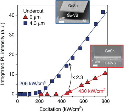
Figure 5 Integrated PL intensity versus optical excitation power (L–L curve) for etched mesa Fabry–Perot laser before (triangles) and after (squares) partial underetching of the mesa. The insets show SEM micrographs illustrating the two configurations.
The latter is remarkable since the underetched mesa structure has an inferior thermal contact to the substrate due to the narrow GeSn film and the remaining part of the Ge virtual substrate (marked as Ge-VS in Fig. 4). Rough estimates of the actual temperature of the GeSn laser due to the high pumping power suggest a realistic temperature of more than 100 K above the measured temperature, indicating operation close to room temperature.
Due to the lattice relaxation of the underetched mesa structures, lasing was obtained for GeSn films having a Sn concentration of 8.5%. Changing the Sn concentration from 8.5% to 14% gives a tuning range of the emission wavelength from 2 to 2.6 µm, as illustrated in Fig. 6. Generally, the emission spectra of the underetched devices are slightly shifted toward longer wavelengths compared to those of the simple mesa type Fabry–Perot waveguide devices. This shift is attributed to relaxation of the residual strain in the freestanding parts of the underetched structures. The lattice relaxation was also detected in micro-Raman measurements.

Figure 6 Emission spectra of optically pumped GeSn laser. Fabry Perot cavities were fabricated by defining mesa structures in the GeSn film and subsequent underetching. The emission wavelength shifts from 2 to 2.6 µm for increasing the Sn concentration from 8.5% to 14%.
The temperature dependence of the emission intensity and of emission wavelength has been measured.2 11 The band structure around the Γ point was calculated using the 8-band k·p method including strain effects. Details can be found in the supplementary information of Ref. 2. The temperature dependence of the PL intensity was simulated, which includes the calculation of the joint density of states, with the band offset ΔE between the minima of Γ and L valleys being the key fitting parameter. By fitting a large amount of experimental PL data from GeSn samples with different Sn concentrations and residual strain, measured by RBS and X-ray diffraction (XRD), a set of parameters used in the 8-band k·p method was established. Figure 7 shows the key results of this self-consistent band structure calculation. Figure 7(a) shows the dependence of the Sn concentration required to obtain a direct bandgap on the residual compressive strain in the GeSn film. Accordingly, a Sn concentration of 8.5% is required in order to obtain a fundamental direct bandgap in fully relaxed GeSn films. Figure 7(b) shows the calculated electronic band structure as function of compressive strain for a specific Ge0.875Sn0.125 alloy. Here the maximum ΔE of about 80 meV is obtained for zero strain and the material becomes indirect once the compressive strain exceeds −1%.
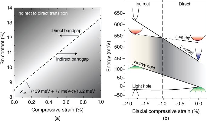
Figure 7 Image (a) shows the dependence of the Sn concentration required to obtain a direct bandgap on the residual compressive strain in the GeSn film. Image (b) shows the calculated electronic band structure as function of compressive strain for a Ge0.875Sn0.125 alloy.
4 Potential of GeSn alloys for electronic devices
The above-described fitting methodology to obtain band structure parameter for the 8-band k·p method was in turn used to calculate the effective mass of electrons in GeSn. Figure 7 shows that for relaxed GeSn with a direct bandgap (Sn content >8.5%), the Γ valley forms the conduction band edge, which is expected to harbor low effective mass electrons and a low density of states. For relaxed GeSn the valence band is degenerate. Adding compressive strain shifts the heavy holes up in energy, whereas tensile strain does the same to the light holes. Tensile strain is accessible by applying a SiNx stressor material to the GeSn film. Figure 8 depicts the calculated effective mass for electrons in the GeSn alloys as a function of residual compressive strain for three Sn concentrations: 8.5%, 12.5%, and 14%. In calculating the in-plane mass mX* (open symbols) and out-of-plane mass mZ*, we find the lowest masses for relaxed GeSn with higher Sn content. Interestingly, the m* for relaxed Ge0.86Sn0.14 is 0.024m0, close to the effective electron mass of InAs.

Figure 8 Effective mass of electrons in the Γ valley versus Sn concentration and compressive strain.
Figure 9(a) shows the calculated room-temperature mobility of electrons in the Γ valley of relaxed GeSn with 12.5% Sn content, including band nonparabolicity as well as phonon scattering. The calculation reveals extremely high mobilities, up to 250,000 cm2/V·s for relaxed GeSn. However, due to the small separation of Γ and L valleys, electrons in both valleys have to be considered. The higher mass and lower mobility of electrons in the L valley, shown in Fig. 9(b), reduce the overall mobility to about 80,000 cm2/V·s – see Fig. 9(c). These calculations do not include alloy scattering, which may have an impact even at room temperature for very high-mobility electrons. Still, it appears likely that GeSn may have electron mobilities competitive with InAs and hole mobilities comparable to Ge. Hence GeSn may offer high-mobility p- and n-MOS circuitry within the same layer and may thus be a strong alternative for the combination of III/V n-MOS with Ge p-MOS, especially since electronic and optoelectronic devices can be integrated as well. Finally, the combination of a group IV alloy having a direct bandgap and very low effective charge carrier masses might be a viable route for high-performance, ultralow-power TFET devices.12 In addition to improved tunneling currents compared to Si TFETs,13 the problem of deep traps due to anti-side defects in III/V compounds, which leads to trap-assisted tunneling, is not present in group IV alloys.

Figure 9 Electron mobility of electrons in the Γ and L valleys versus residual compressive strain for a GeSn alloy containing 12.5% Sn.
5 Conclusion
RGSE was employed to grow GeSn alloys up to 14%, thus far beyond the solid solubility limit of 1% Sn in Ge. The RGSE technique enables growth at high rates and low deposition temperatures while maintaining pristine crystallographic quality. Optically pumped lasers were fabricated from GeSn films deposited on Ge virtual substrates. Underetching of the waveguide structures led to drastic improvement of the laser performance, cutting the threshold pump power by half and increasing the efficiency by a factor of 2.3. Lasing was observed up to 135 K. The experimental data on the optical properties were used to fine-tune the parameter set for k·p bandstructure calculations. Relaxed GeSn alloys with Sn concentrations exceeding 8.5% exhibit a direct fundamental bandgap. The electrons in the Γ valley are predicted to have very low effective masses and high mobilities, making GeSn a potential alternative material for high-speed, low-power electronics. Hence, GeSn may offer a versatile platform for EPIC.
Acknowledgments
The above-presented work summarizes the in-depth collaboration with a large number of scientists. S. Wirths and N. von den Driesch (PGI-9, FZJ) grew the samples by RGSE. R. Geiger and H. Sigg (Paul Scherrer Institute, CH) and S. Wirths performed PL and optical pumping measurements. D. Stange and T. Stoica performed PL investigations at FZJ. J.-M. Hartmann (CEA-LETI, France) supplied the Ge virtual substrates. M. Luysberg (ER-C and PGI-5, FZJ) performed TEM measurements. J. Faist (ETH-Zürich) calculated the optical waveguide properties. Z. Ikonic (Leeds University) led the effort in bandstructure calculations of GeSn alloys (Figs. 7–9). G. Mussler and B. Holländer (PGI-9, FZJ) did extensive XRD and RBS measurements. D. Buca and S. Mantl scientifically supervised and coordinated the GeSn team at PGI-9, FZJ.
References
- 1. C. H. L. Goodman, “Direct-gap group IV semiconductors based on tin,” IEE Proc. I: Solid State Electron Dev. 129, 189–192 (1982).
- 2. S. Wirths, R. Geiger, N. von den Driesch, et al., “Lasing in direct-bandgap GeSn alloy grown on Si,” Nature Photonics 9, 88–92 (2015).
- 3. K.-H. Koo and K. C. Saraswat, “Study of performances of low-κ Cu, CNTs, and optical interconnects,” chapter in: N. K. Jha and D. Chen, eds., Nanoelectronic Circuit Design, New York: Springer, 2011, pp. 377–407.
- 4. P. Moontragoon, R. A. Soref, and Z. Ikonic, “The direct and indirect bandgaps of unstrained SixGe1−x−ySny and their photonic device applications,” J. Appl. Phys. 112, 073106 (2012)
- 5. R. Soref, “Direct-bandgap compositions of the CSiGeSn group-IV alloy,” Opt. Mater. Express 4, 836–842 (2014).
- 6. S. Wirths, D. Buca, G. Mussler, et al., “Reduced pressure CVD growth of Ge and Ge1−xSnx alloys,” ECS J. Solid State Sci. Technol. 2, N99–N102 (2013).
- 7. Y. Shimura, N. Tsutsui, O. Nakatsuka, A. Sakai, and S. Zaima, “Low temperature growth of Ge1−xSnx buffer layers for tensile-strained Ge layers,” Thin Solid Films 518, S2–S5 (2010).
- 8. S. M. Gates and C. M. Chiang, “Dissociative chemisorption mechanisms of disilane on Si(100)-(2×1) and H-terminated Si(100) surfaces,” Chem. Phys. Lett. 184, 448–454 (1991).
- 9. F. Gencarelli, B. Vincent, L. Souriau, et al., “Low-temperature Ge and GeSn chemical vapor deposition using Ge2H6,” Thin Solid Films 520, 3211–3215 (2012).
- 10. N. von den Driesch, D. Stange, S. Wirths, et al., “Direct bandgap group IV epitaxy on Si for laser applications,” Chem. Mater. 27, 4693–4702 (2015).
- 11. D. Stange, S. Wirths, N. von den Driesch, et al., “Optical transitions in direct bandgap Ge1−xSnx alloys,” ACS Photonics 2, 1539–1545 (2015).
- 12. S. Wirths, A. T. Tiedemann, Z. Ikonic, et al., “Band engineering and growth of tensile strained Ge/(Si)GeSn heterostructures for tunnel field effect transistors,” Appl. Phys. Lett. 102, 192103 (2013).
- 13. L. Knoll, Q.-T. Zhao, A. Nichau, et al., “Inverters with strained Si nanowire complementary tunnel field-effect transistors,” IEEE Electron Device Lett. 34, 813–815 (2013).