
1.8
Nanomanufacturing for Electronics or Optoelectronics
M. J. Kelly
Department of Engineering, Centre for Advanced Photonics and Electronics, University of Cambridge, 9 JJ Thomson Avenue, CB3 0FA, Cambridge, United Kingdom; MacDiarmid Institute for Advanced Materials and Nanotechnology, Victoria University of Wellington, Wellington, 6140, New Zealand
1 Introduction
Artefacts in widespread use in electronic and optoelectronic systems have been manufactured by low-cost, high-volume processes. To get to that stage, the understanding and design of the artefact and the choice of materials are such that several key attributes apply1:
- The artefacts exhibit performance that is superior to what went before, or are otherwise much cheaper for the same performance.
- A high yield to an acceptable tolerance is achieved, with in-batch uniformity and interbatch reproducibility.
- A functional simulator is available for reverse engineering during development and right-first-time design in production.
- The artefacts are reliable and have an adequate service lifetime.
While we recognize these features, for example, in products for mainstream applications, we also note their absence in many, but not all, nanoscale artefacts made with comparable fabrication technologies such as deposition, etching, and lithography.
In practice, one can apply also this argument to complex molecules as nanoscale artefacts. If one translates six-sigma quality into four or five-nines purity, only a few relatively simple molecules are available at >99.99% purity, the level one would require if one were to make integrated circuits from such molecules in some bottom-up process, such as laying out a memory array based on such molecules as storage nodes. Here we are considering just the starting ingredients, before any considerations of a defect-free array of such molecules.
While the move from three-dimensional electronic systems to two-dimensional (2D) systems (the quantum well, the 2D electron gas, etc.) has produced new physics and a wide range of new devices in widespread applications, the same is not true for one- or zero-dimensional electronic systems, and this insignificant part is because the level of reproducibility is inadequate for low-cost, high-volume production. In this chapter, we review recent progress and lack of progress on manufacturability of several nanoscale systems using the above criteria: tunnel devices, split-gate transistors/quantum point contacts, and other nanoscale systems.
2 Nano-LEGO®
A good test example2 is to consider a conventional LEGO® brick, typically a few tens of mm on each side, when scaled down by a factor of 10N for N < 7. In Fig. 1, we show typical brick sizes as a function of the center-to-center pitch, P, of the pillars on the topside. We will assume a simplified underside where just the hole to receive the cylinders is retained, leaving the brick otherwise solid, rather than hollow as in conventional LEGO. A brick with a skin of only a few nanometers thickness would be too fragile. The manufacturing tolerance for conventional bricks is 10 µm, or typically of order 1/1000 of the brick size. This is used to allow tight mating of adjacent ricks and the possibility of building a tall vertical stack. Relaxing this tolerance at smaller scales is essential and compromising the ability to use the resulting bricks for assembling structures. At each scale we can consider the methods for (i) one-off fabrication, (ii) volume production, and (iii) the assembly and disassembly of structures, comprising on the order of 103 bricks, such as a scale model of the Eiffel Tower. Table 1 shows how first the practical use is constrained by the decreased size, then the reliability of manufacture and ultimately the reliability of even one-off fabrication.
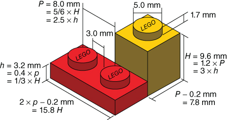
Figure 1 Dimensions of standard Lego® bricks,
(Source: see http://www.lucasbrouwers.nl/blog/2011/05/why-life-is-like-lego/ CC BY-SA 3.0).
Table 1 Milli-, micro-, and nanobricks. The scale is set in comparison with real LEGO® bricks of Fig. 1; fabrication and manufacture techniques include IM(p) as injection molding of plastic, IS(p) as imprint stamping of plastic, and DLE(s) as deposition, lithography, and etching of semiconductors
| Scale | Fabricate | Manufacture | Can use/user tool | Comment on use |
| 1 (mm) | IM(p) | IM(p) | Yes/hands | Easy |
| 10−1 | IM(p) | IM(p) | Yes/tweezers | Straightforward |
| 10−2 | IS(p) | IS(p) | Yes/microtweezers | Tricky |
| 10−3 (µm) | IS(p), DLE(s) | IS(p), DLE(s) | Yes/microtweezers, AFM | Demanding |
| 10−4 | IS(p), DLE(s) | IS(p), DLE(s) | Yes/AFM | Only at relaxed tolerances |
| 10−5 | IS(p), DLE(s) | None | None | Impossible |
| 10−6 (nm) | AFM | None | None | Impossible |
As the downscaling proceeds, the ability to use fails first, to manufacture fails second, and to fabricate fails last. The use fails for several reasons, one being the tolerance at 1/1000 is less easily scaled, another being the inability to construct a stable tower 100 bricks high at the 1 µm scale. Note that there are at least two technologies – (i) imprint stamping and (ii) deposition, lithography, and etching –that persist as fabrication technologies scale down to the nanoscale. There are many further aspects that can be considered instructively at each scale: yield, reproducibility, wear and tear, etc.
This exercise is one that all candidate artefacts for nanoscale manufacture must undertake successfully.
3 Tunnel devices
Over the 40 years since tunneling and resonant tunneling was observed in thin barriers in semiconductor multilayers, there have been many device prototypes exploiting tunneling that exhibit superior figures of merit for switching and amplifying in both electronics and optoelectronics. There are functional simulators that can be used to model tunneling in devices and to reverse-engineer experimental results. The only problem has been the lack of in-wafer uniformity and wafer-to-wafer reproducibility, within and between growth runs, of the basic device characteristics.
Over the last 23 years, I have worked with various collaborators on this issue and we have recently made progress that achieves the required uniformity and reproducibility for a single AlAs barrier in GaAs designed for use as a millimeter-wave detector. Tunnel currents are very sensitive to the height and thickness of the tunnel barrier, with a 270% variation for a change in thickness of a single monolayer. It is exceedingly difficult to reach a prespecified target current–voltage characteristics with a <5% spread and with wafer-to-wafer reproducibility within 5%. Figure 2 presents maps3 of the current for a fixed forward bias across 100 µm square diodes from two wafers grown that the same time in a RIBER V100HU MBE production growth machine that have a standard deviation in the electrical properties of 1% or less and a wafer average that differs by less than 1%. This result was achieved by taking a growth process that includes very slow growth of integer monolayer barriers proven on a research machine, where the interwafer and intergrowth uniformity for devices on the same part of a wafer were the same within a few percent,4 but with a remaining cross-wafer linear trend of 20% in the current–voltage characteristics that remains from the off-axis geometry of the MBE aluminum source in the growth chamber. The process is now being examined in the context of double-barrier structures, as together with the detector diode, we have the elements of a high-efficiency but low-power communication system for operation up to 0.5 THz.

Figure 2 Wafer maps showing the current measured on (∼320) 100 µm square diodes at a forward bias of 0.5 V. Note the extreme uniformity compared with previous reports.5 6 For both wafers, the standard deviation of the currents across the wafer is ∼1% of the average current, and the average currents from the two wafers agree within 1%. Note: seven wafers were grown on a platen at a time in a configuration of a central wafer (D) and six around it (of which A is one): hence the claim of uniformity equivalent to a single 8 in. wafer. The black spaces are fields protected for further use. The mask has 10 subfields each with 32 100-µm square diodes, all of which have been measured: there is one mesa measured per pixel in the diagrams.
4 Split-gate transistors
Since the invention of the split-gate transistor (or quantum point contact) in 1986 and its subsequent use to discover the quantization of the one-dimensional ballistic resistance, most studies have used single gates or a few gates to investigate physics in 1D wires and laterally confined quantum dots. In terms of manufacturability, only one heroic study of 540 split-gate devices made in batches of 36 of different wafers gave any insight into the reproducibility of the quantization phenomenon in and between devices.7 A part of the problem is the limited number of wires that can be taken from the cryostat for external measurements.
We have developed a first-generation multiplexing geometry that allows an array of 256 devices to be addressed with less than 20 wires – see Fig. 3(a).8 We can distinguish between fabrication yield (94%), which can be improved to 100% with greater experience and attention to detail, and quantum yield (76% going to 84% when illuminated) of actual ballistic quantization steps. This yield reflects something of the detailed distribution of donor atoms in the supply layer of the transistor, and various forms of disorder or interference that can mask the clear steps. We have been able to collect and evaluate the average and standard deviation of the pinch-off voltage (Fig. 3(b)) and the voltage at which the 1D/2D transition takes place. The average slope of the ladder of 1D steps is a measure of the local density of the 2D electron gas, and this has a standard deviation of 4% for devices that are typically a 100 µm apart. This places limitations on inferences from simple Hall bar measurements on the actual local electron density for 1D phenomena.

Figure 3 (a) The principle of the multiplexer where the nontrivial addition to the standard split-gate geometry is the layer of dielectric under some gates, shown as a gray area, that allows a bias to be applied to various lines without the underlying 2DEG being pinched off. (b) Normalized plots of the spatial distribution of the pinch-off voltage VP of the split-gate transistors on two successive cooldowns showing the level of continuity of properties of each gate. Black areas denote failed devices. The vertical (horizontal) pitch of the actual devices is 130 µm (100 µm).
This initial multiplexer is used for gathering statistics of the device operation, which are now being used to try to distinguish between various explanations of the so-called 0.7 spin phenomenon.9 A second generation of multiplexer allows each gate to be biased and charge to be held on each gate before an experiment is undertaken. The first application is to investigate phenomena in a 2 × 7 array of closely coupled quantum dots.10
For any real-world applications, such as in charge pumps for quantum metrology or specific quantum information processing systems, one needs a strategy to narrow the standard deviation of the device parameters. One intriguing possibility is to zero every gate to the pinch-off condition before starting any experiment, and an algorithm to achieve this has been developed. Of the attributes specific to manufacturability, reproducibility needs further improvement, simple simulations are available, and reliability and service life can be inferred from earlier cryogenic experiments.
5 Other nanoscale systems
Unlike the case of tunneling, consideration of quantum dot manufacturing has not advanced in the 3 years since the last FTM conference.11 In the case of such applications as quantum key sources of single photons, one must search the surface for the particular dot at the required wavelength without guaranteeing its optimum positioning in any subsequent cavity.12
There are many examples of papers working on the new forms of carbon, fullerenes, nanotubes, and graphene, but these are still in the realms of one-offs in terms of individual or few devices, or very small and primitive integrated circuits. Issues such as yield and reproducibility to a prespecified performance remain as yet unstudied. The same applies to other quasi-monolayer electron systems.
6 Conclusion
In selected areas, there has been some progress toward the manufacturing of nanoscale artefacts. The remaining concern is living with the intrinsic fluctuations from one nanoscale artefact to the next, and whether there can be any design-around to cope these fluctuations.
Acknowledgments
This work is done with several teams of collaborators, listed as coauthors of the referenced papers, and funded by the Engineering and Physical Science Research Council of the United Kingdom over 20 years, and the Royal Society's Mercer Innovation Fund more recently.
References
- 1. M. J. Kelly, “Intrinsic top-down unmanufacturability,” Nanotechnology 22 234303 (2011).
- 2. M. J. Kelly and M. C. Dean, “A specific nanomanufacturing challenge,” Nanotechnology 27, 112501 (2016).
- 3. M. Missous, M. J. Kelly, and J. Sexton, “Extremely uniform tunnel barriers for low-cost device manufacture,” IEEE Electron Device Lett. 36, 543–545 (2015).
- 4. C. Shao, J. Sexton, M. Missous, and M. J. Kelly, “Achieving reproducibility needed for manufacturing semiconductor tunnel devices,” Electronics Lett. 49, 669–671 (2013).
- 5. V. A. Wilkinson, M. J. Kelly, and M. Carr, “Tunnel devices are not yet manufacturable,” Semicond. Sci. Technol. 12, 91–99 (1997).
- 6. R. K. Hayden, A. E. Gunnaes, M. Missous, R. Khan, M. J. Kelly, and M. J. Goringe, “Ex-situ re-calibration method for low-cost precision epitaxial growth of heterostructure devices,” Semicond. Sci. Technol. 17, 135–140 (2002).
- 7. Q. Z. Yang, M. J. Kelly, H. Beere, I. Farrer, and G. A. C. Jones, “The potential of split-gate transistors as one-dimensional electron waveguides revealed through the testing and analysis of yield and reproducibility,” Appl. Phys. Lett. 94, article no. 033502 (2009).
- 8. H. Al-Taie, L. W. Smith, B. Xu, et al., “Cryogenic on-chip multiplexer for the study of quantum transport in 256 split-gate devices,” Appl. Phys. Lett. 102, 243102 (2013).
- 9. L. W. Smith, H. Al-Taie, F. Sfigakis, et al., “Statistical study of conductance properties in one-dimensional quantum wires focusing on the 0.7 anomaly,” Phys. Rev. B 90, 045426 (2014).
- 10. R. K. Puddy, L. W. Smith, H. Al-Taie, et al., “Multiplexed charge-locking device for large arrays of quantum devices,” Appl. Phys. Lett. 107, 143501 (2015).
- 11. M. J. Kelly, “Manufacturability and nanoelectronic performance,” chapter in: S. Luryi, J. Xu, and A. Zaslavsky, eds., Future Trends in Microelectronics: Frontiers and Innovations, New York: Wiley, 2013, pp. 133–138.
- 12. M. C. Dean and M. J. Kelly, “The manufacturability of self-assembled quantum-dot-based devices,” unpublished.