
1.6
A Universal Nonvolatile Processing Environment
T. Windbacher, A. Makarov, V. Sverdlov and S. Selberherr
Institute for Microelectronics, TU Wien, 1040 Vienna, Austria
1 Introduction
After many decades of stunning progress in the shrinking of complementary metal-oxide-semiconductor (CMOS) devices, the steadily increasing difficulty in handling physical limitations as well as the rapidly increasing production and investment costs for each new technology generation will stop CMOS scaling in the not-too-distant future. Among the most challenging problems for further performance gains today are the static power dissipation as well as the interconnection delay and the associated energy for information transport.1 2 A very efficient solution to the static leakage power problem is to simply turn off unused parts of a circuit. However, this causes the previously stored information to vanish and requires energy- and time-wasting recovery cycles, when the dormant circuit parts are powered up. Thus, in order to avoid information loss during shutdown, nonvolatile elements must be incorporated.
Due to its CMOS compatibility, nonvolatility, high endurance, and fast operation, spintronics is a promising avenue for adding nonvolatility to circuits.3 The term spintronics is very general and covers a vast number of devices with an extreme variety in operating principles and practical feasibility for commercial applications.3 4 In this chapter, we concentrate on what, in our opinion, appears to be the most feasible technology for large-scale integration in the next few years: the combination of CMOS with nonvolatile magnetoresistive random-access memory (MRAM). Indeed, the integration of CMOS and magnetic tunnel junctions (MTJs) is not only likely but already available in the form of nonvolatile stand-alone MRAM arrays and embedded DRAM,5 and the introduction of further commercial products will surely follow.6–9
Importantly, the all-electrical magnetization manipulation in modern MRAM by spin transfer torque (STT) renders the wires for separate magnetic field generation superfluous and also significantly reduces the MTJ switching energy. Technological advances, such as the exploitation of free-layer perpendicular magnetic anisotropy and use of MgO tunnel barriers, have led to a further reduction in switching energy, as well as improved scalability.10 Promising spintronic solutions with respect to speed and power consumption have been able to compete with CMOS-only solutions.9 11
However, the usual CMOS/MTJ hybrid structures use MTJs only for storage, while the actual computation is still carried out via CMOS logic. The addition of MTJs also increases circuit complexity and footprint, as extra transistors are needed to read and write the MTJs to access the stored memory data.
2 Universal nonvolatile processing environment
Shifting the actual computation into the magnetic domain would help not only to simplify the layout but also increase the integration density. We propose a universal nonvolatile processing environment, schematically illustrated in Fig. 1, consisting of spin torque majority gates (STMGs)12 and nonvolatile magnetic flip-flops,13 illustrated in Figs 2 and 3, respectively. By arranging the STMGs and flip-flops in an array, the flip-flops can be exploited as shared buffers available for neighboring STMGs. In order to elaborate the concept further, a possible realization of an easily extendable 1-bit full adder with the aid of just a single STMG and three nonvolatile flip-flops is explained in the following section.

Figure 1 The spin torque majority gates (crosses) perform the computation, while the nonvolatile flip-flops (rectangles) act as shared buffers. A single STMG and three flip-flops are sufficient to realize a concatenated 1-bit full adder.

Figure 2 The nonvolatile magnetic flip-flop comprises three synthetic antiferro-magnetic polarizer stacks with perpendicular magnetization orientation. Two polarizer stacks, A and B, are for inputs and one polarizer stack Q is for readout. They are connected via nonmagnetic interconnection layers to a common free magnetic layer featuring a uniaxial perpendicular magnetic anisotropy.

Figure 3 The STMG shares the basic structural features with the nonvolatile flip-flop but exhibits a cross-like common free layer and four polarizer stacks (A, B, C for input and Q for readout). The device is operated via polarity-encoded current pulses and the result of an operation is stored by the magnetization orientation of the free layer. The stored information can be accessed either by using the TMR or GMR effect or by employing the common free layer as a polarizer for a neighboring device.
To fully understand the operation of the nonvolatile processing environment, one has to address first the operation principle of the devices as well as how the information is transferred between them. As illustrated in Figs 2 and 3, the devices are basically spin valves (nonmagnetic metal interconnection layers) or MTJs (oxide interconnection layers) with a common free layer. Thus, these devices are operated via current pulses and the polarities of the applied pulse represent the two logic states “0” and “1,” respectively. The flip-flop has two inputs A and B. Four input combinations are possible. Depending on the applied pulse polarity in relation to the free layer orientation, the acting torque either drives growing precessions, which may lead to a change in the magnetization orientation, or it damps the magnetization movement and tries to keep it in its current position. In the case of two synchronous input pulses with the same polarity, two spin-polarized currents enter the free layer and cause two STTs acting in the same fashion. They add up and cause either the set or the reset of the common free layer orientation. On the other hand, if two synchronous input pulses with opposing polarities are applied, the two torques compensate each other and the initial magnetization orientation is preserved (hold operation). The STMG has the same operation principle, but instead of two input pulses there are always three synchronous pulses. Thus, for any input combination there is always at least one uncompensated STT contribution that prevails and determines the final state of the common free layer. This behavior replicates the majority function12 and can facilitate combinational logic. One has to note that the majority function requires additionally the logic negation to form a computationally complete basis. The simplest solution for this is to assume that the not operation is carried out by inverting the polarity of the corresponding input pulse.
Finally, it is necessary to elucidate how information is transferred between these devices. As already pointed out above, the key to the operation is the orientation and interaction of the applied torques. Therefore, by applying a current pulse to one of the overlapping regions between neighboring devices, the electrons entering the first common free layer are polarized along the first layer's magnetization orientation – see Fig. 4. When they cross over into the second free layer, they relax to the magnetization orientation in the second free layer and by that create an STT encoded with the information stored in the first free layer. Since it takes much longer for a free layer to switch with one active input compared to the case when all inputs are active, there is a safe time window for copying information from a free layer without switching its magnetization.

Figure 4 By performing a well-defined set of majority, not, and copy operations, an easily concatenable 1-bit full adder is realized. The overlapping region between the common free layers of the flip-flops and the STMG can be employed to first polarize electrons entering a free layer and then, when crossing over to an adjacent free layer of a neighboring device, to create a spin transfer torque orientation encoded with the information stored in the previous layer.
The assumed 1-bit full adder exhibits three inputs A, B, and CIN and two outputs Sum and COUT. Furthermore, the logic function for the sum is given by14
and the carry-out bit COUT is defined as
Due to the computational completeness of the proposed processing environment, any logic function can be transformed into a sequence of well-defined majority and not operations. For instance, in a first step one calculates majority[A, B, CIN], with the resulting carry-out bit COUT subsequently copied into one of the adjacent flip-flops (e.g., FF1). In the next step, majority[A, B, not(CIN)] is performed and stored in another flip-flop (FF2). Finally, the sum bit is obtained by executing majority[not(FF1), FF2, CIN] and moving the result into FF3. Thus, COUT and Sum are stored and accessible via FF1 and FF3, respectively. Since we chose to perform the calculation of COUT in the very first step, it can be already used by FF1's neighboring STMG as CIN even before the calculation of sum is finished. In this way, the calculation is parallelizable and the exploitation of the flip-flops as shared local buffers reduces significantly information transport over the global bus.
3 Bias-field-free spin-torque oscillator
A further essential building block in modern electronics is the oscillator.14 Unfortunately, spin-torque oscillators often require an external magnetic field or operate only at relatively low frequencies, which limits their practical implementation. Previously, we demonstrated that the nonvolatile magnetic flip-flop device intrinsically provides a spin-torque oscillator.15 It operates without an external magnetic field at high frequencies and complements perfectly the proposed nonvolatile processing environment, thereby boosting the achievable integration density. In direct comparison to a CMOS ring oscillator (see Fig. 5) at an assumed half pitch of 15 nm, our proposed structure is approximately 30 times smaller.3 15

Figure 5 Circuit diagram for a minimal ring oscillator. The ring oscillator comprises an odd number of inverter stages (in this case three), where each output is fed to the input of the following stage. Above a certain supply voltage VDD the circuit starts to oscillate.
In order to boost the output power as well as the operation frequency, a structure comprising two three-layer MTJ stacks with a shared free layer was proposed – see Fig. 6.16 The oscillation frequency of the structure can be tuned by varying the amplitude of the applied current density of one of the MTJs, while the other one is kept fixed, as shown in Fig. 7. In this way, frequencies of up to 30 GHz can be excited.17

Figure 6 Schematic illustration of a spin-torque oscillator based on two MTJs. The arrows indicate the direction of the current for each of the MTJs.
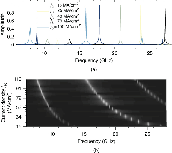
Figure 7 Illustration of the signal spectral density with normalized peak values. The length of the shared free layer has been set to 40 nm and the current density through MTJB was changed between 1.5 × 10⁷ and 1.1 × 10⁸ A/cm2, while keeping the current density for MTJA fixed at jA = 2.05 × 10⁸ A/cm2.
Furthermore, the oscillation spectrum contains a primary mode at frequency f and a secondary mode at frequency f/2. By increasing the applied current density jB through MTJB, the amplitude of the secondary mode starts to increase and eventually reaches more than half the maximum amplitude of the primary mode, whereas the output power of the primary mode decreases. There is also a significant dependence of the excited modes on the geometry of the free layer, shown in Fig. 8. Structures with free layer lengths ranging from 40 to 60 nm and current density combinations between 107 and 2.05 × 10⁸ A/cm2 have been investigated.

Figure 8 The geometrical dependence of the oscillation regime versus applied current density jA through MTJA (jB ≤ jA/2) for free layers of 40, 45, 50, 55, and 60 nm. Current density combinations for which the secondary oscillation mode f/2 reaches more than 50% of the primary mode f are shown in light gray.
Increasing the length of the free layer and thereby the distance between the MgO-MTJs shifts the region where the additional large-amplitude oscillation mode appears in the direction of larger jA/jB ratios. Thus, the largest variation in the current density at which the additional mode does not reach large amplitudes is observed in the structure with a 40 nm free layer length.
4 Summary
The resulting nonvolatile processing environment features a highly regular structure, is computationally complete, and reduces the information transport due to its shared buffers. Thus, it is viable for a universal post-CMOS logic technology. The flip-flop is very versatile. The same device can be used stand alone or stacked for even higher integration density. It also offers the possibility of being used as a bias-field-free oscillator while preserving an extremely small footprint. For these reasons, we believe the presented processing environment and its components are very promising candidates for pushing the achievable integration density beyond the state-of-the-art CMOS-MTJ hybrids, while keeping the dissipated power and interconnection delay in check.
Acknowledgments
This research is supported by the European Research Council through the Grant #247056 MOSILSPIN.
References
- 1. International Technology Roadmap for Semiconductors, chapter PIDS (2013) available at http://www.itrs.net (accessed on Apr. 11, 2016).
- 2. R. Marculescu, U. Ogras, L.-S. Peh, N. Jerger, and Y. Hoskote, “Outstanding research problems in NoC design: System, microarchitecture, and circuit perspectives,” IEEE Trans. CAD Integr. Circ. Syst. 28, 3–21 (2009).
- 3. D. Nikonov and I. Young, “Overview of beyond-CMOS devices and a uniform methodology for their benchmarking,” Proc. IEEE 101, 2498–2533 (2013).
- 4. W. Zhao and G. Prenat, eds., Spintronics-Based Computing, New York: Springer, 2015.
- 5. See Everspin website (2015) available at www.everspin.com/mram-replaces-dram (accessed on Apr. 11, 2016).
- 6. Y. Zhang, W. Zhao, W. Kang, E. Deng, J.-O. Klein, and D. Revelosona, “Current-induced magnetic switching for high performance computing,” chapter in: W. Zhao and G. Prenat, eds., Spintronics-Based Computing, New York: Springer, 2015, pp. 1–51.
- 7. E. Deng, Y. Zhang, W. Kang, B. Dieny, J.-O. Klein, G. Prenat, and W. Zhao, “Synchronous 8-bit non-volatile full-adder based on spin transfer torque magnetic tunnel junction,” IEEE Trans. Circ. Syst. I 62, 1757–1765 (2015).
- 8. E. Deng, W. Kang, Y. Zhang, J.-O. Klein, C. Chappert, and W. Zhao, “Design optimization and analysis of multicontext STT-MTJ/CMOS logic circuits,” IEEE Trans. Nanotechnol. 14, 169–177 (2015).
- 9. W. Zhao, L. Torres, Y. Guillemenet, et al., “Design of MRAM based logic circuits and its applications,” ACM Great Lakes Symp. VLSI (2011), pp. 431–436.
- 10. S. Ikeda, J. Hayakawa, Y. Ashizawa, et al., “Tunnel magnetoresistance of 604% at 300 K by suppression of Ta diffusion in CoFeB/MgO/CoFeB pseudo-spin-valves annealed at high T,” Appl. Phys. Lett. 93, 082508 (2008).
- 11. D. Chabi, W. Zhao, E. Deng, Y. Zhang, N. B. Romdhane, J.-O. Klein, and C. Chappert, “Ultra low power magnetic flip-flop based on checkpointing/power gating and self-enable mechanisms,” IEEE Trans. Circ. Syst. I 61, 1755–1765 (2014).
- 12. D. E. Nikonov, G. I. Bourianoff, and T. Ghani, “Proposal of a spin torque majority gate logic,” IEEE Electron Device Lett. 32, 1128–1130 (2011).
- 13. T. Windbacher, H. Mahmoudi, V. Sverdlov, and S. Selberherr, “Spin torque magnetic integrated circuit,” WIPO WO 2014/154997 A1 (published Oct. 2, 2014).
- 14. U. Tietze and C. Schenk, Electronic Circuits – Handbook for Design and Applications, 2nd ed, New York: Springer, 2008.
- 15. T. Windbacher, A. Makarov, H. Mahmoudi, V. Sverdlov, and S. Selberherr, “Novel bias field-free spin transfer oscillator,” J. Appl. Phys. 115, 17C901 (2014).
- 16. A. Makarov, V. Sverdlov, and S. Selberherr, “Concept of a bias-field-free spin-torque oscillator based on two MgO-MTJs,” Extended Abstracts SSDM (2013), pp. 796–797.
- 17. A. Makarov, T. Windbacher, V. Sverdlov, and S. Selberherr, “Efficient high-frequency spin-torque oscillators composed of two three-layer MgO-MTJs with a common free layer,” Proc. 21st Iberchip Workshop (2015).