
1.5
Challenges to Ultralow-Power Semiconductor Device Operation
Francis Balestra
IMEP-LAHC, Minatec, Grenoble-Alpes University, 38016 Grenoble Cedex 1, France
1 Introduction
The historic trend in micro-/nanoelectronics over the last 40 years has been to increase both speed and density by scaling down the electronic devices, together with reduced energy dissipation per binary transition, and to develop many novel functionalities for future electronic systems. We are facing today dramatic challenges for “more Moore” and “more than Moore” applications: substantial increase of energy consumption and heating that can jeopardize future IC integration and performance, reduced performance due to limitation in traditional high-conductivity metal/low-κ dielectric interconnects, limit of optical lithography, heterogeneous integration of new functionalities for future nanosystems, and so on.
Therefore, many breakthroughs, disruptive technologies, novel materials, and innovative devices are needed in the next two decades.
With respect to the substantial reduction of the static and dynamic power of future high-performance/ultralow-power terascale integration logic and autonomous nanosystems, new materials and novel device architectures are mandatory for ultimate complementary metal-oxide-semiconductor (CMOS) and beyond-CMOS eras, as well as new circuit design techniques, architectures, and embedded software.
Alternative memories, especially PCRAM, RRAM, or MRAM will be useful for pushing the limit of integration and performance beyond those afforded by present nonvolatile, DRAM and SRAM memories.
In the interconnect area, optical and RF interconnects, carbon or other 2D materials can overcome the present limitations of copper interconnects for power consumption and performance.
Concerning ultimate processing technologies, extreme ultraviolet (EUV) lithography, immersion multiple patterning, multi-e-beam maskless or imprint lithography, as well as self-assembly of nanodevices could be used for different applications.
Future autonomous nanosystems will also need the development of nanoscale high-performance novel functionalities, which could be integrated on CMOS platforms. In this respect, nanostructures and nanodevices, especially nanowires (NWs), are of great interest, for instance, for improving the sensitivity, resolution, selectivity, energy consumption, and response time of nanosensors, and for solar, mechanical, and thermal energy harvesting.
Parallel or sequential processes could be used for the integration of these future high-performance and low-power sustainable, secure, ubiquitous and pervasive systems, which will be of high added value for many applications in the field of (autonomous) detection and communication of health problems, environment quality and security, secure transport, building and industrial monitoring, entertainment, education, and so on.1–14
This chapter focuses on the main trends, challenges, limits, and possible solutions for ultralow-power nanoscale devices in the CMOS and beyond-CMOS arena, including many novel materials, ultrathin films, multigates, nanowires, and small slope switches.
2 Ultimate MOS transistors
The slowdown of VDD scaling and the substantial increase of the subthreshold leakage lead to a dramatic enhancement of the dynamic and static power consumption. This power challenge is due to the subthreshold slope limit S, which is 60 mV/dec at room temperature for MOSFETs. A lower limit in energy per operation can be reached with minimum VDD ∼ S and minimum E ∼ CS2, where C is the device capacitance, as illustrated schematically in Fig. 1.15

Figure 1 Lower limit in energy per operation obtained for optimal drain bias VDD.
There are several ways of reducing the swing SS, given by
One can decrease of the transistor body factor m, using ultrathin body silicon-on-insulator (SOI), multigate or nanowire MOSFETs, carbon nanotube or 2D channels (leading to m ∼ 1), and negative capacitance field-effect transistors (FETs), or MEMS/NEMS structures (leading to m < 1). Alternatively, one can resort to low-temperature operation, which cannot be applied to traditional applications. Finally, one can modify the carrier injection mechanisms by turning to impact ionization or band-to-band tunneling (BTBT).
In the field of MOSFETs, several very interesting advances have been recently reported. Ultrathin semiconductor films and 3D-FETs can improve sub-20 nm CMOS node performance and substantially reduce supply voltage and short channel effects.
The best MOSFET devices leading to SS close to its minimum value are using fully depleted channels16–19 (e.g., FD-SOI with very thin buried oxide19) or fully inverted ones with volume inversion20 that is even more effective into optimizing electrostatic control21 of the structure (e.g., double-gate (DG), bulk, or SOI tri-gate/fin-FET, gate-all-around (GAA) MOSFET or nanowire FET).
The first fully depleted SOI MOSFETs have been fabricated on SOS materials16 but with Si films of poor quality. The first FD-SOI MOSFET with an ideal swing of about 60 mV/dec was demonstrated by numerical simulation in 1985 (see Fig. 2).17 The first experimental demonstration of an FD-SOI MOSFET with SS ∼ 60 mV/dec followed in 1986.18

Figure 2 Transfer ID(VG) characteristics obtained by numerical simulation for fully depleted n- and p-channel SOI MOSFETs showing a 60 mV/dec subthreshold swing (10−14 Si doping, 600 nm Si film).17
Short channel effects (DIBL and charge sharing) in multigate MOSFETs are also reduced with decreasing the silicon film thickness tSi (down to 5 nm) and doping, regardless of whether the architecture is single- or DG (see Fig. 3). Furthermore, a reduced sensitivity to tSi and doping is observed for the DG devices, which is promising for the optimization of their electrical properties.21

Figure 3 DIBL effect versus silicon film thickness tSi for LG = 50 nm devices: single-gate SOI MOSFETs (tOX1 = 380 nm; tOX2 = 3 nm) with high doping (NA = 5 × 1017 cm−3, VG2 = 0), low doping (NA = 1015 cm−3, VG2 = 0), back channel accumulation (NA = 1015 cm−3, VG2 = −40 V); and for double-gate SOI MOSFETs (tOX1 = tOX2 = 3 nm, NA = 1015 cm−3 and NA = 5 × 1017 cm−3 with VG1 = VG2).
DG devices with gate underlap have also shown to lead to a very good ID, a reduction in the drain-induced barrier lowering (DIBL) and drain-to-gate leakage current, and a decrease in propagation delay and power.22
Small diameter (3 nm) nanowire FETs have demonstrated experimentally very good ION/IOFF performance,23 with the best SS ∼ 75 mV/dec obtained by numerical simulation down to 5 nm gate length for both strained Si and InGaAs channel materials, as shown in Fig. 4.24
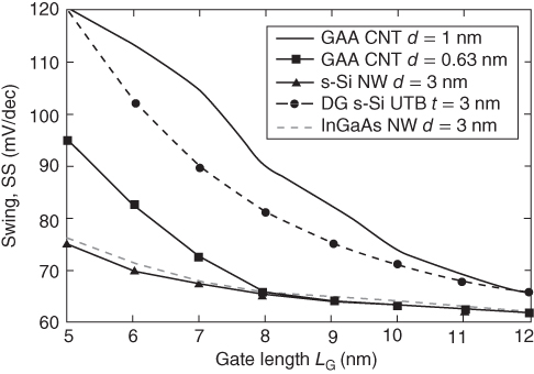
Figure 4 Subthreshold swing SS obtained by quantum transport numerical simulation as a function of device architecture for gate length LG down to 5 nm: double-gate strained-Si ultrathin-body MOSFET (tSi = 3 nm), Ω-gate strained-Si and InGaAs nanowires with 3 nm diameter, gate-all-around carbon nanotubes (GAA CNTs) with 1 and 0.63 nm diameters.
In addition to III–V materials, there are other high-mobility materials that may replace Si in future VLSI applications. In this respect, heterogeneous 2D atomic crystals, especially transition-metal dichalcogenides (TMDs), have atomically smooth surface without dangling bounds or thickness fluctuations, as well as good mobility in chemical vapor deposition (CVD)-deposited films. They are thus very attractive enablers of ultimately scaled transistors and 3D ICs. The first CMOS-compatible TMD 3D transistor technology using novel hybrid Si/MoS2 channel fin-FET and NW FET was demonstrated recently (see Fig. 5).

Figure 5 Si/MoS2/HfO2/TiN hybrid fin-FET (a) and nanowire transistor (b).
These 3D TMD transistors exhibit improved electron mobility compared to Si-based 3D FETs as well as higher drive current ION, as illustrated in Figs 6 and 7, respectively.25 It has also been shown that MoS2 FETs can meet high-performance (HP) requirement up to 6.6 nm node by employing bilayer MoS2 as the channel material, while low-standby-power (LSTP) requirements present significant challenges for sub-10 nm nodes. On the other hand, the high mobility and the low effective mass of tungsten diselenide (WSe2) may enable 2D FETs for both HP and LSTP applications down to the 5 nm node.

Figure 6 Field effect mobility of n-type Si/MoS2 fin-FET showing a substantial increase compared with Si fin-FET.

Figure 7 Improvement of ION current drive for hybrid Si/MoS2 devices compared with Si fin-FET and NW FETs as a function of the number of MoS2 layers.
The subthreshold swing and DIBL were evaluated for both DG and SOI structures from monolayer (1L) to three-layer (3L) MoS2, and compared to Si-based ultrathin-body (UTB) DG FETs. It was shown that MoS2 FETs generally have better electrostatics than Si devices. Single-gate SOI topology can only sustain good electrostatics for 1L TMDs, while DG topology can present interesting performance for up to 3L TMDs, as shown in Fig. 8.26

Figure 8 (a) Subthreshold swing and (b) DIBL versus LG scaling for MoS2 FETs realized with 1, 2, or 3 monolayers, compared to Si-based UTB DG FETs with a symmetrical top and bottom gate dielectric (in SOI the bottom dielectric is 50 nm thick SiO2 and the bottom gate is grounded).
Carbon nanotube FETs, with a very good control of short channel effects and with the highest current drive to-date (>100 µA/µm at 400 nm channel length and 1 V drain bias) have been demonstrated while simultaneously achieving reasonable ION/IOFF > 5000.27
On the other hand, silicon fin-FETs with silicided source/drain, exploiting biased Schottky barriers, have been demonstrated. By combining a positive feedback induced by weak impact ionization with a dynamic modulation of the Schottky barriers, the device achieves a minimal subthreshold slope of 3 mV/dec and an average subthreshold slope of 6.0 mV/dec over 5 dec of current at room temperature. However, a drain bias of several volts is needed.28
A comparative analysis of ring oscillators based on different channel materials, different spacer materials, and different transistor architectures suggests that the largest benefits of speed gain and power consumption reduction for MOSFET architectures is achieved by switching from 7 nm Si baseline fin-FET process to 5 nm vertical Si NWs.29
Another interesting possibility at the end of the roadmap could be to use semimetals for channel and source/drain. Indeed, for 1D devices, the band gap of semiconductors and semimetals increases with decreasing NW diameter. Therefore, a semimetal could become a semiconductor in the sub-10 nm range, as shown in Fig. 9. In this case, 1D structures could be used for the channel and thicker metallic source/drain regions could be made from the same material (e.g., Sn, Bi) without any extrinsic doping. Very good electrical properties have been shown by ab-initio simulations for 1 nm GAA Sn NWs with a 2.3 nm gate length, leading to a 72 mV/dec swing and ION ∼ 3 mA/µm at VD = 250 mV.30

Figure 9 Band gap versus NW diameter for various semiconductors and semimetals.
3 Small slope switches
In the domain of small slope switches, the tunneling field-effect transistors (TFETs) seem very promising. However, so far, no one has demonstrated experimentally a TFET that has simultaneously both an ION comparable to a CMOS FET and a subthreshold swing of less than 60 mV/dec for several decades. The highest current for which a subthreshold swing of 60 mV/dec is observed is approximately 10 nA/µm. While the experimentally observed ION are in reasonable agreement with theoretical predictions, there is disparity in the subthreshold characteristics due to the fact that simulations usually neglect nonidealities and defects and that these advanced technologies using novel materials, technologies, and device architectures have to be optimized.31
The originally studied TFET configurations also suffered from low ION current levels usually in the order of few µA/µm caused by the misalignment of the tunneling direction and the gate-induced electric field. A new class of TFETs was introduced in which both BTBT direction and gate electric field are kept parallel, which allows ION to be proportional to the gate length. Among such transistors, the electron–hole bilayer tunneling field-effect transistor (EHBTFET) was proposed to exploit BTBT between a 2D electron gas and a 2D hole gas. Tunneling between 2D regions was demonstrated to be the most advisable scenario to optimize switching behavior. Semiclassical simulations for Ge EHBTFET showed impressive results that later on needed to be corrected for quantum mechanical effects and parasitic lateral tunneling and its undesired implications for the device performance.
It has been demonstrated that the inclusion of quantum confinement in Ge EHBTFET gives rise to the appearance of tunneling paths misaligned with the gate electric field that were not present in the semiclassical framework. This unwanted leakage between the overlap and underlap regions of the device reduced the steepness of the I–V curves and degraded SS. To overcome this problem, a heterogate EHBTFET may provide a potential solution to suppress the lateral tunneling in the subthreshold region while maintaining the high ION due to vertical BTBT in the overlap region.32
Simulated DG TFETs with 2D layers using MoS2–WTe2 vertical tunneling, shown in Fig. 10, also showed very good subthreshold swing.33

Figure 10 Proposed MoS2–WTe2 double-gate TFET structure.
Finally, TFETs realized with III–V materials, for example, InAs, strained InAs, GaSb–InAs heterostructures, graded AlGaSb source H-TFET and quantum well (QW) InAs–GaSb source with InAs channel have been compared by quantum simulations. The best results were obtained for the QW-TFET, with graded source TFET coming second, and both significantly outperforming the reference MOSFET – see Fig. 11.34
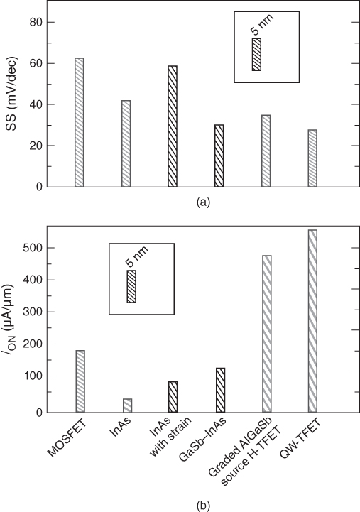
Figure 11 Comparison of MOSFETs performance (current drive ION and subthreshold swing SS) with InAs TFET, strained InAs TFET, GaSb–InAs heterostructure TFET, graded source AlGaSb–InAs HTFET, and QW InAs–GaSb–InAs TFET. In all cases, IOFF is set at 5 nA/µm.
4 Conclusion
We are facing dramatic challenges dealing with future nanoscale devices, including performance, power consumption, new materials, device integration, interconnects, ultimate technological processes, and novel functionalities, needing disruptive approaches and inducing fundamental trade-offs for future ICs and nanosystems. This chapter reviewed recent advances and promising solutions for future ultralow power devices combining novel materials and innovative device architectures, including 2D layers, TMDs, heterostructures and quantum wells using strained Si, Ge, and III–V thin films, as well as multigate, nanowire, CNT transistors, and tunnel FETs.
Acknowledgments
The author would like to thank the Sinano Institute Members and Partners of Nanosil and Nanofunction FP7 European Networks of Excellence.
References
- 1. F. Balestra, ed., Nanoscale CMOS: Innovative Materials, Modeling and Characterization, London: ISTE-Wiley, 2010.
- 2. F. Balestra, ed., Beyond CMOS Nanodevices, vols. 1 and 2, London: ISTE-Wiley, 2014.
- 3. J. Brini, M. Benachir, G. Ghibaudo, and F. Balestra, “Subthreshold slope and threshold voltage of the volume inversion MOS transistor,” Proc. IEE Part G: Circ. Devices Syst. 138, 133–136 (1991).
- 4. F. Balestra, M. Benachir, J. Brini, and G. Ghibaudo, “Analytical models of subthreshold swing and threshold voltage for thin and ultra-thin film SOI MOSFETs,” IEEE Trans. Electron Devices 37, 2303–2311 (1990).
- 5. F. Conzatti, M. G. Pala, D. Esseni, E. Bano, and L. Selmi, “A simulation study of strain induced performance enhancements in InAs nanowire tunnel-FETs,” Tech. Dig. IEDM (2011), p. 95.
- 6. G. Dewey, B. Chu-Kung, J. Boardman, and J. M. Fastenau, “Fabrication, characterization and physics of III–V heterojunction tunneling FET for steep subthreshold swing,” Tech. Dig. IEDM (2011), p. 785.
- 7. J. Appenzeller, Y.-M. Lin, J. Knoch, and Ph. Avouris, “Band-to-band tunneling in carbon nanotube field-effect transistors,” Phys. Rev. Lett. 93, 193805 (2004).
- 8. A. Padilla, C. W. Yeung, C. Shin, C. Hu, and T.-J. King Liu, “Feedback FET: A novel transistor exhibiting steep switching behavior at low bias voltages,” Tech. Dig. IEDM (2008), p. 171.
- 9. K. Boucart, A. M. Ionescu, and W. Riess, “Asymmetrically strained all-silicon tunnel FETs featuring 1 V operation,” Proc. ESSDERC (1989), p. 452.
- 10. F. Mayer, C. Le Royer, J.-F. Damlencourt, et al., “Impact of SOI, Si1−xGexOI and GeOI substrates on CMOS-compatible tunnel FET performance,” Tech. Dig. IEDM (2008), pp. 1–5.
- 11. D. Esseni and M. G. Pala, “Interface traps in InAs nanowire tunnel FETs and MOSFETs – Part II: Comparative analysis and trap-induced variability,” IEEE Trans. Electron Devices 60, 2802–2807 (2013).
- 12. S. Brocard, M. Pala, and D. Esseni, “Design options for hetero-junction tunnel FETs with high on current and steep sub-threshold voltage slope,” Tech. Dig. IEDM (2013), p. 5.4.1.
- 13. M. H. Lee, J.-C. Lin, Y.-T. Wei, et al., “Ferroelectric negative capacitance hetero-tunnel field-effect-transistors with internal voltage amplification,” Tech. Dig. IEDM (2013), p. 104.
- 14. S. Brocard, M. Pala, and D. Esseni, “Large on-current enhancement in hetero-junction tunnel-FETs via molar fraction grading,” IEEE Trans. Electron Devices 35, 184–186 (2014).
- 15. S. Hanson, M. Seok, D. Sylvester, and D. Blaauw, “Nanometer device scaling in subthreshold logic and SRAM,” IEEE Trans. Electron Devices 55, 175–185 (2008).
- 16. F. Balestra, J. Brini, and P. Gentil, “Deep depleted SOI MOSFETs with back potential control: A numerical simulation,” Solid State Electron. 28, 1031–1037 (1985).
- 17. F. Balestra, Characterization and Simulation of SOI MOSFETs with Back Potential Control, PhD thesis, INP-Grenoble, 1985.
- 18. J. P. Colinge, “Subthreshold slope of thin-film SOI MOSFETs,” IEEE Electron Device Lett. 7, 244–246 (1986).
- 19. F. Andrieu, O. Weber, J. Mazurier, O. Thomas, J.-P. Noel, and C. Fenouillet-Béranger, “Low leakage and low variability ultra-thin body and buried oxide (UT2B) SOI technology for 20 nm low-power CMOS and beyond,” Proc. VLSI Symp. (2010), pp. 57–58.
- 20. F. Balestra, S. Cristoloveanu, M. Benachir, J. Brini, and T. Elewa, “Double-gate silicon-on-insulator transistor with volume inversion: a new device with greatly enhanced performance,” IEEE Electron Device Lett. 8, 410–412 (1987).
- 21. E. Rauly, O. Potavin, F. Balestra, and C. Raynaud, “On the subthreshold swing and short channel effects in single and double gate deep submicron SOI MOSFETs,” Solid State Electron. 43, 2033–2037 (1999).
- 22. A. Bansal, B. C. Paul, and K. Roy, “Impact of gate underlap on gate capacitance and gate tunneling current in 16 nm DGMOS devices,” Proc. IEEE SOI Conf. (2004), pp. 94–95.
- 23. C. Dupré, A. Hubert, S. Becu, et al., “15 nm-diameter 3D stacked nanowires with independent gates operation: ΦFET,” Tech. Dig. IEDM (2008), p. 549.
- 24. M. Luisier, M. Lundstrom, D. A. Antoniadis, and J. Bokor, “Ultimate device scaling: Intrinsic performance comparisons of carbon-based, InGaAs, and Si FETs for 5 nm gate length,” Tech. Dig. IEDM (2011), p. 251.
- 25. M.-C. Chen, C.-Y. Lin, K.-H. Li, et al., “Hybrid Si/TMD 2D electronic double channels fabricated using solid CVD few-layer-MoS2 stacking for Vth matching and CMOS-compatible 3DFETs,” Tech. Dig. IEDM (2014), p. 808.
- 26. W. Cao, J. Kang, D. Sarkar, W. Liu, and K. Banerjee, “Performance evaluation and design considerations of 2D semiconductor based FETs for sub-10 nm VLSI,” Tech. Dig. IEDM (2014), p. 729.
- 27. M. M. Shulaker, T. F. Wu, A. Pal, et al., “Monolithic 3D integration of logic and memory: Carbon nanotube FETs, resistive RAM, and silicon FETs,” Tech. Dig. IEDM (2014), p. 812.
- 28. J. Zhang, M. De Marchi, P.-E. Gaillardon, and G. De Micheli, “A Schottky-barrier silicon FinFET with 6.0 mV/dec subthreshold slope over 5 decades of current,” Tech. Dig. IEDM (2014), p. 339.
- 29. V. Moroz, L. Smith, J. Huang, et al., “Modeling and optimization of group IV and III–V fin-FETs and nanowires,” Tech. Dig. IEDM (2014), p. 180.
- 30. L. Ansari, G. Fagas, J.-P. Colinge, and J. C. Greer, “A proposed confinement modulated gap nanowire transistor based on a metal (tin),” Nano Lett. 12, 2222–2227 (2012).
- 31. H. Lu and A. C. Seabaugh, “Tunnel field-effect transistors: State-of-the-art,” J. Electron Devices Soc. 2, 44–49 (2014).
- 32. J. L. Padilla, C. Alper, F. Gámiz, and A. M. Ionescu, “Assessment of pseudo-bilayer structures in the heterogate germanium electron-hole bilayer tunnel field-effect transistor,” Appl. Phys. Lett. 106, 262102 (2015).
- 33. K.-T. Lam, G. Seol, and J. Guo, “Performance evaluation of MoS2–WTe2 vertical tunneling transistor using real-space quantum simulator,” Tech. Dig. IEDM (2014), p. 721.
- 34. M. Pala and S. Brocard, “Exploiting heterojunctions to improve the performance of III–V nanowire tunnel-FETs,” IEEE J. Electron Devices Soc. 3, 115–121 (2015).