
2.2
Graphene and Atom-Thick 2D Materials: Device Application Prospects
Sungwoo Hwang, Jinseong Heo, Min-Hyun Lee, Kyung-Eun Byun, Yeonchoo Cho and Seongjun Park
Device Laboratory, Samsung Advanced Institute of Technology, Suwon, 443-803, South Korea
1 Introduction
The electronic properties of low-dimensional systems have long been an interesting topic in both physics and engineering societies. Silicon MOSFET and III–V HEMT devices, for example, not only have been the most essential elements in micro- and nanoelectronics since their early days but have also provided wonderful playgrounds for correlated 2D electron systems, leading to such fundamental discoveries as the integer and fractional quantum Hall effects. These traditional 2D electron systems have now reappeared in the form of atomic sheets, shedding light on entirely new physics originating from the orbital confinement, as well as new materials science aspects. The new physics, in turn, enables innovation in the 2D device realm. In this chapter, we consider these new opportunities and accompanying challenges, examining various aspects of potential device applications of graphene and atom-thick 2D materials, including optoelectronic devices, new types of transistors, and possible CMOS integration. Direct growth is the key technology to make all these applications realistic, so we will also address the prospects of wafer-scale graphene and 2D materials growth.
2 Conventional low-dimensional systems
Back in 1967,1 Stern and Howard considered the two-dimensional electron gas (2DEG) at the Si/SiO2 interface, where the electron wavefunction is confined within a few nanometers in the direction perpendicular to the interface. High-mobility 2DEG was then created in III–V HEMTs by Stormer et al. in 1979.2 Physicists utilized these 2DEGs as a wonderful playground for new types of electronic states. The integer quantum Hall effect,3 a manifestation of magnetic field-induced localization–delocalization transition, was observed at the Si/SiO2 interface. Subsequently, the fractional quantum Hall effect4 arising in strongly correlated 2D electron liquids was found in high-mobility HEMTs. These observations were only made possible by superb quality of the devices. In 1981, when integer quantum Hall effect was first observed, Intel was already manufacturing processors with more than 100,000 transistors. Advances in large-scale CMOS circuits have been driving modern information technology to this date.
If the electronic wavefunction of a 2DEG is further confined, one can realize a one-dimensional electron gas (1DEG). In 1988, van Wees et al.5 fabricated 1DEGs by placing split gates on a III–V HEMT and defining a narrow electron channel by negatively biasing these gates. The mobility of the HEMT wafer was 106 cm2/V·s, resulting in the mean free path of several microns at 4 K making it possible to observe conductance quantization whenever the gate voltage opened a new conductance channel. Scott-Thomas et al.6 fabricated silicon 1DEGs by the double-gate technique and observed Coulomb blockade oscillations. These early 1DEGs studied for fundamental physics have now reappeared in such devices as fin-FETs7 and gate all-around (GAA) Si nanowire FETs,8 illustrated in Figs. 1 and 2, respectively, as examples of ultimate highly scaled Si MOSFETs.

Figure 1 Schematic structure of a fin-FET.

Figure 2 (a) Gate-all-around Si nanowire MOSFET; and (b) transconductance as a function of gate length.
(Source: Cho et al.8 Reproduced with permissions of the American Institute of Physics).
Figure 2 also shows the conductance measured as a function of gate bias VG in GAA Si nanowire FETs with length ranging from 400 to 20 nm. It shows conductance overshoot when the channel length is shorter than 40 nm. This length scale is comparable to the mean free path of electrons in Si at room temperature, providing strong evidence of ballistic transport. One well-known but important message is that the device performance will not be improved much in these nodes even though we scale the channel length.
3 New atomically thin material systems
Newly discovered atom-thick 2D systems, including graphene, can be thought of as a traditional 2DEG shrunk to atomic thickness. The extreme orbital confinement manifests itself in new physics originating from material aspects and dimensional confinement on the atomic scale. The new physics is giving us many new opportunities for creating new device functionalities and innovating conventional 2D devices.
Graphene, one isolated sheet of graphite or a honeycomb 2D lattice of carbon atoms, was discovered by Geim and Novoselov in 2004.9 In layered graphite, each carbon atom has sp2 hybridization, leading to strong intralayer covalent bonding and relatively weak van der Waals interlayer interaction, with an interlayer distance of 0.34 nm. Such weak bonding between layers leads to simple mechanical exfoliation using adhesive tape, resulting in atomically thin monolayers of carbon atoms (see Fig. 3(a) and (b)). Having linear energy–momentum dispersion relation, shown in Fig. 3(c), low energy excitations of carriers in graphene mimic relativistic Dirac particles with a reduced velocity of c/300, called massless Dirac fermions.10 A simple consequence of this unique dispersion is the absence of backscattering, leading to mobility up to 200,000 cm2/V·s at room temperature. More excitingly, many novel physical effects have been explored experimentally: half-integer quantum Hall effect,9 Coulomb drag (frictional coupling between electric currents flowing in spatially separated conducting layers due to interlayer electron–electron interactions),11 and Hofstadter's butterfly effect,12 when 2D electrons in both a magnetic field and a periodic electrostatic potential exhibit a self-similar recursive energy spectrum.

Figure 3 (a) Highly oriented pyrolysis graphite (HOPG) with adhesive tape; (b) exfoliated graphene on SiO2/Si substrate; and (c) electronic band structure of graphene and linear dispersion at K points in the Brillouin zone.
In addition to new fundamental physics, graphene has a number of superior technological properties in terms of transparency, bulk resistivity, current density, chemical inertness, surface area, and thermal conductivity. Graphene has high transparency of 97.7% over a wide spectral range, bulk resistivity of 10 µΩ cm, and can carry current densities of 106 A/cm2, compared to 1.68 µΩ cm and 4020 A/cm2 for Cu of monolayer thickness, respectively. It also has chemical inertness from aromatic bonds of 518 bond enthalpies kJ/mol compared to 348 for C—C bond; a high surface area of 2630 m2/g compared to 500 for activated carbon; and thermal conductivity of 5300 W/m·K, compared to 2320 for diamond. These properties can be combined and exploited in transparent electrodes, interconnects, barrier materials, supercapacitor, and heat sink applications – see Fig. 4. For example, transparent electrodes require both high transparency and low sheet resistance. Doped four-layer graphene has 30 Ω/![]() sheet resistance at 90% transparency, superior to commercial indium tin oxides.13 Moreover, for flexible applications, graphene-based transparent electrode can withstand strains of more than 6%, whereas ITO cracks under 2–3% strain. As another example, heat management in modern integrated chips or CPUs is becoming increasingly important because of ever-larger heat dissipation as device density increases. Given a thermal conductivity of around 40 times larger than Si, graphene is expected to provide viable solutions for heat management in modern integrated chips when incorporated in the form of composites or inks.
sheet resistance at 90% transparency, superior to commercial indium tin oxides.13 Moreover, for flexible applications, graphene-based transparent electrode can withstand strains of more than 6%, whereas ITO cracks under 2–3% strain. As another example, heat management in modern integrated chips or CPUs is becoming increasingly important because of ever-larger heat dissipation as device density increases. Given a thermal conductivity of around 40 times larger than Si, graphene is expected to provide viable solutions for heat management in modern integrated chips when incorporated in the form of composites or inks.

Figure 4 Properties of graphene and its applications.
Since its discovery in 2004, graphene has been at the center of new materials research both in academia and industry for disruptive innovation. However, for applications such as flexible digital electronics, new functional nanomaterials beyond graphene are required, with such properties as an electronic bandgap or atomically clean dielectric interfaces. The search for other layered materials that can be easily exfoliated has produced a large number of 2D materials besides graphene. These include monoatomic phosphorene and diatomic materials such as hexagonal boron nitride (h-BN) and transition metal dichalcogenides (TMDCs)14 – see Table 1. While graphene is a semimetal, some TMDCs are semiconducting, whereas h-BN is a dielectric with an ultraclean surface. The most studied semiconducting TMDCs are MoS2 (see Fig. 5 for bandstructure), MoSe2, WS2, and WSe2. From the optoelectronic application viewpoint, these 2D materials span the range from zero bandgap graphene to a large bandgap semiconductor such as GaS (∼3 eV), to the insulator h-BN. In addition to aforementioned basic components, there is also a new class of materials such as 2D superconductors, for example, NbS2 and NbSe2. With a whole library of 2D materials and their heterostructures, one can envisage a new atomic system with a broad range of functionalities.15

Figure 5 Band structure of (a) monolayer; (b) bilayer; and (c) bulk MoS2.
Table 1 Some examples of layered 2D materials
| Semimetal/superconductor | Graphene, WTe2, PtSe2, TiS2 | NbS2, NbSe2 |
| Topological insulator/insulator | Bi2S3, Bi2Se3, Bi2Te3 | h-BN |
| Semiconductor | Black phosphorus, MoS2, MoSe2, MoTe2, WS2, WSe2, GaS, GaS2, HfS2, HfSe2, In2Se3, ReS2, ReSe2, ZrSe2, SnS2, SnSe2, TiSe2, TaS2, GeS | |
4 Device application of new material systems
• Photodetectors
Two-dimensional materials provide strong light-matter interaction, such that even a single monolayer can have up to 10% absorption, depending on wavelength and material bandgap.16 With large absorption coefficients of 105–106 cm−1 of 2D materials in the visible range, almost two orders of magnitude larger than Si, photodetectors based on 2D materials can be made as thin as a few tens of nanometers. One of the photodetector figures of merit is responsivity or external quantum efficiency, which measures the number of electrons generated per incident photon.17 Focusing on vertically stacked photodetectors with a transparent electrode/photoactive region/electrode sequence, a responsivity of 20 A/W was measured in graphene/MoS2/graphene heterostructures (see Table 2).
Table 2 Performance of various 2D heterojunction photodetectors
| Material stack | Measurement conditions | R (A/W) | tR (ms) | References |
| G/WSe2/G | VD = 0.5 V, VG = 0, λ = 514 nm, P = 10−5 µW/µm2 | 0.33 (1.1) | <30 (28 × 10−3) | 18 |
| G/MoS2/G | VD = 5 V, VG = 30 V, λ = 633 nm, P = 0.24 µW/µm2 | 20 | >104 | 18 |
| G/WS2/G | VD = 0, VG = −20 V, λ = 488 nm, P = 10 µW/µm2 | 0.1 | NA | 19 |
| G/MoS2/G | VD = 0 V, VG = −60 V, λ = 514 nm, P = 80 µW/µm2 | 0.06 | NA | 20 |
| G/WSe2/MoS2/G | VD = 0, VG = 0, λ = 532 nm, P = 3−7 µW/µm2 | 0.12 | NA | 21 |
Another figure of merit of photodetectors is response time or bandwidth, a critical measure for optical communication. Graphene has the highest mobility and ultrabroadband photoresponse but only absorbs 2.3% of light.22 The weak absorption of graphene can be overcome by integrating it with a Si waveguide in order to enhance the detection area along the propagation direction23–25 (see Fig. 6).

Figure 6 (a) Schematic of graphene–Si waveguide photodetector and its cross section with field intensity; (b) By design, the optical field is maximized at the interface between Si and graphene.
Graphene/Si hybrid photodetectors showed a 3 dB bandwidth of 20 GHz at 1550 nm wavelength. Monolayer deposition of graphene on a Si waveguide offers simpler and cheaper integration than heteroepitaxial growth of III–V or Ge layers on Si for upcoming all-optical chips.
• New types of transistors
Graphene FETs showed unprecedented mobility of over 100,000 cm2/V·s at room temperature,26 two orders of magnitude larger than Si CMOS. As a result, graphene was considered a candidate for future electronics in post-Si era. But graphene lacks a bandgap of at least a few hundred millielectron volts, making it difficult to switch off the FET current. A number of graphene-based alternatives have been proposed – graphene nanoribbons,27 bilayer graphene with tunable bandgap,28 and graphene nanomeshes,29 – but all have suffered from either lithographically patterned irregular edges, the absence of uniformity and controllability over large area, or small on/off current ratios.
The challenges of using standalone graphene for digital applications shifted the focus to graphene hybrid systems. In order to attain an appropriate energy barrier to turn off charge flow, semiconducting materials were brought in contact with graphene. For example, graphene–Si hybrid junctions make Schottky diodes where the barrier height of the junction can be tuned by gate voltage as the workfunction of graphene is modulated (see Fig. 7).30 This solid-state triode system, called graphene barristor, enabled high on/off ratio of 105 and a half-adder circuit was demonstrated upon its integration.

Figure 7 Graphene barristor and its operation principle.
The work on graphene barristors also demonstrated a new finding: the absence of pinning in graphene on Si. This unique property can be applied to reduce source–drain contact resistance, which is discussed in Section 5.2. Graphene/2D semiconductor heterotunnel junctions were also demonstrated to show large on/off ratio31 and atomically thin semiconductors, such as WS2, sandwiched between graphene layers, led to transparent and flexible tunneling transistors.32 Recent results in this area are summarized in Table 3. Graphene–semiconductor–metal tunnel junctions on 8-in. wafer scale provide a versatile platform to be tailored by varying materials and deposition thicknesses for low-power electronics, as in Fig. 8.35
Table 3 Performance of vertical tunneling transistors based on 2D materials
| Materials | ION at 0.5 V (µA/µm2) | ION/IOFF | SS (mV/dec) | References |
| G/IGZO/Mo | 10 | 106 | 30–1,000 | 18 |
| G/MoS2/Ti | 10 | 103 | 20,000 | 33 |
| G/WS2/G | 5 | 106 | 10,000 | 32 |
| Pt/Al2O3/G/Si | 10−6 | 106 | 250 | 34 |

Figure 8 Graphene–semiconductor–metal tunneling junction transistors (SAIT).
• Challenges
It should be noted that many conceptually new device concepts that appeared in the ITRS, including carbon nanotubes, single electron transistors, and spin MOSFETs, have not to date succeeded in displacing Si technology. In that regard, the new graphene- and/or other atom-thick 2D material-based optoelectronic or electronics devices discussed above could require many years before showing up in the market.36 Even though they show higher photoresponsivity and optical communication speeds, as well as on/off ratios comparable to conventional devices, there are still many challenges to overcome.
As far as heterojunctions are concerned, there is the perennial question of interfaces. First of all, large-scale graphene grown on germanium37 or catalytic metal surfaces38 has to be transferred to the target substrate, including exposed Si or other 2D materials. The transfer process usually involves adhesives, polymers, or chemical etchants,39 which in turn introduce organic, ionic, or metal residues. Spatial variation of these residues degrades device uniformity and controllability. Second, there is the 2D semiconductor and metal contact issue. With lack of precise doping control for both p- and n-type 2D semiconductors, true Ohmic contact is difficult to achieve. So far, only limited chemical doping has shown some reduction of contact resistance,40 but the results are still inferior to state-of-the-art Si technology. Third, there is no thorough study on scaling of two-dimensional devices including both channel and contact area. Even though the best ION of 10 µA/µm2 at 0.5 V for 2D heterojunction tunnel devices is comparable to state-of-the-art Si contact resistivity, all aforementioned issues result in nonuniform distribution and degradation of on-current for electronic devices.
5 Components in Si technology
So far, we discussed devices based on active functions of graphene or related 2D materials for optoelectronic or electronic applications that might be adopted in 5–10 years. More realistic application of those materials is implementation as a component layered material in Si device process, enhancing device performance.
The first MOSFET, patented in 1960 by D. Kang41 and shown in Fig. 9, was a flat device using only Si, SiO2, and Al as constituent materials. Continued performance improvement and dimensional scaling of MOSFETs during last half century have been made possible only by continuously adopting new type of structures, materials, and processing technologies. Compared to Fig. 9, a modern CMOS device architecture, shown in several chapters of this book, is replete with tremendous complications and adaptations. The Al interconnect was replaced by Cu for the lower parasitic resistance in the late 1990s, in spite of the high diffusivity of Cu into active device regions and the deep defect level of Cu in Si. Also, the damascene process was adopted to solve the difficulty in etching Cu.42 Then, SiO2/poly-Si gate was replaced by high-κ/metal gate stack for scaling the equivalent oxide thickness (EOT) from the 45 nm technology node onward, regardless of the difficulties in threshold voltage (VT) alignment and complex new process steps, such as atomic layer deposition (ALD).43 Two-dimensional atom-thick materials hold potential promise as passive components in following two possible scenarios in sub-10 nm technology node.

Figure 9 The original Si MOSFET41 patent.
• Interconnects
The exponential increase in the number of interconnects and their increasing resistance with device downscaling have always comprised a major limiting factor for fabricating more complex electronic device. Until the recent sub-20 nm nodes, additional Cu metal layers and the damascene process provided reasonable resistance and manufacturability in the back-end-of-line (BEOL) process flow. However, shrunken Cu interconnects have to carry higher current densities, resulting in migration, deformation, or diffusion to other regions because of increased heat dissipation. Moreover, electron scattering at the surfaces and grain boundaries, as well as line edge roughness (LER), start to play an increasing role in the conduction properties of metal, and the effective resistivity of Cu more than doubles as the line width decreases from 100 to 10 nm.44 Furthermore, the thickness of the liner/barrier layer has remained almost constant and the portion of liner/barrier layer in interconnect has increased from 1% to 50%.45
There are few possible ways to overcome these issues: improvement of the effective resistivity of Cu by increasing grain size and decreasing LER, hybridization or replacement of interconnect material with lower resistivity materials, and introduction of an atomically thin liner/barrier layer. Chemical vapor deposition of graphene on catalytic metals38 is a well-known method for large-scale and high-quality graphene film production. Among other metals, Cu offers the best quality of monolayer graphene because of near-zero solubility and self-terminated growth mechanism.46 As a result, Cu–graphene hybrid interconnect appears a promising alternative to Cu alone, and graphene-covered Cu brings a lot of benefits. Since graphene is both a good electrical and thermal conductor, and a good barrier material, graphene–Cu interconnects can prevent electromigration and provide increased current-carrying capacity – see Fig. 10. These concepts were patented47 by IBM, Toshiba, and others and published in a few of papers.48 49 For example, Yeh et al. reported the current-carrying capacity of 22 nm-node interconnect was increased from 1.1 × 10⁸ to 1.1 × 10⁹ A/cm2 when Cu was replaced by graphite–Cu grown at 400 °C.49

Figure 10 (a) Graphene–Cu interconnect patent;47 and (b) TEM image for graphene–Cu interconnect structure (SAIT).
(Source: http://www.google.co.uk/patents/US3102230. Public domain).
Finally, full replacement of Cu by graphene can be expected at line widths of a few nanometers.50 Experimentally, graphene shows a peak current capacity on the order of 108 A/cm2 and the comparable resistivity to Cu lines scaled below 40 nm.51 52 Also, multilayer graphene intercalated with iron chloride may outperform copper in a current capacity and resistivity (>107 A/cm2, 3.2 µΩ at 8 nm width).48 53
• Source–drain contacts
Scaling issues also challenge the front-end-of-line (FEOL) process. The Si/metal contact resistance increases as the inverse square of the device size, unlike other resistances that increase linearly as the device size decreases. This rapid increase in the contact resistance has led to it to exceed the channel resistance below 32 nm node54 (see Fig. 11). Larger contact resistance in scaled devices prevents optimal scaling of the supply voltage, resulting in greater power consumption.

Figure 11 ITRS target for contact resistance at various technology nodes.
Theoretically, the contact resistance is strongly dependent on the Schottky barrier height, formed by the misalignment between the metal workfunction and the semiconductor affinity of electrons or holes. Thus, low workfunction (∼4.0 eV) metals for n-type Si and high workfunction (∼5.2 eV) metals for p-type Si are supposed to guarantee Ohmic contact behavior and low contact resistance. However, most metals show high measured Schottky barrier heights of about 0.5 eV due to pinning effects at the semiconductor interface. There have been a few candidates for resolving this contact issue by introducing a highly doped Si S/D layers or thin insertion layers between highly doped Si and contact metal. The highly doped Si results in a sufficiently narrow depletion width for effective charge tunneling, and this technique was widely used in current Si devices. However, this method is approaching the dopant solubility limit in semiconductor (<1021 cm−3), and faces challenges in shallow junction formation, high source–drain leakage currents, and low thermal stability. The insertion layer prevents Fermi level pinning between metal and semiconductor, and at the same time, the layer is thin enough that tunneling probability of charges approaches unity. For example, Agrawal et al. reported that 1 nm-thick TiO2−x layer inserted between Ti and n-Si reduces contact resistance by an order of magnitude to 9.1 × 10⁻⁹ Ω cm2.55 However, the insulating layer is hard to control when its thickness falls below 1 nm and the thermal stability on the Si layer may be insufficient.
On the other hand, 2D materials with monolayer thickness less than 1 nm can be an optimal candidate for depinning the interface and maximizing tunneling probability. As mentioned in Section 4.2, the Schottky barrier height between graphene and Si was changed by the same amount as the workfunction of graphene by a gate voltage, proving depinning of the graphene–Si interface.30 This is an attractive property for the Si/metal contact formation. Also, the graphene can reduce the metal workfunction by charge transfer, similar to surface doping.56 This could prove helpful for n-type semiconductor contacts that need a low workfunction below 4 eV (see Fig. 12).

Figure 12 Workfunction of metal-doped graphene and its formation energy as function of distance calculated using density functional theory.
In addition, 2D materials have other attractive features for insertion into contacts: nonpermeability, high thermal stability, and digital thickness control with low predicted Schottky barrier heights, as shown in Fig. 13.57

Figure 13 Predicted Schottky barrier heights for n-type Si of graphene, metals, and graphene-doped metals.
To test the effect of a graphene insertion layer at metal/Si junction, a Si AFM tip was contacted to graphene/Ni and Ni surfaces for comparison in a vacuum chamber.58 As shown in Fig. 14, the Si/Ni junction exhibited rectifying diode-like I–V characteristics, whereas the graphene-inserted junction was Ohmic with low resistance. The measured minimum contact resistance ranged from 10−8 to 10−9 Ω·cm2, comparable to state-of-the-art Si technology.
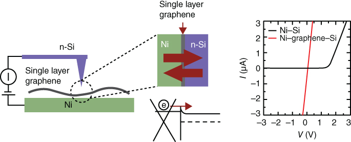
Figure 14 Schematic of conducting AFM experiment for measuring contact resistance of a metal/Si junction with and without graphene (left); band diagram with inserted graphene layer (middle); corresponding I–V curves (right).
6 Graphene on Ge
For most of device applications, direct growth of high-quality graphene and 2D materials on various substrates is the most important issue. Typically, graphene has been grown on metallic catalyst substrates such as Ni38 or Cu.46 For interconnect applications, growth of graphene on insulators such as SiO2 or SiN will be essential. Contact applications require the growth of high-quality graphene or 2D materials directly on the semiconductor surface. Recent reports on the growth of graphene on Si59 and Ge37 60 and growth of MoS2 on fused silica61 are therefore of great interest. Another important aspect is the crystallinity of graphene. Polycrystalline graphene was usually obtained in earlier works on metallic catalysts. Great progress on single-crystal graphene growth has been made using a single seed,62 and recent work using multiple aligned seeds37 represents an interesting breakthrough.
7 Conclusion
Newly emergent 2D materials including graphene and TMDCs began as playgrounds for observing exotic physics, such as unconventional quantum Hall effect and quantum transport phenomena. Just as the fundamental understanding and exploration of conventional 2DEG in an earlier era became the cornerstone of modern IT industry, these atom-thick 2D materials may lead to an industrial revolution in the post-Si era. In particular, for electronic devices, atomically thin tunnel transistors can offer additional transparency and flexibility with comparable performance to Si, whereas for photodetectors 2D materials can provide wider bandwidth and cheaper integration with Si for data communication. They may also provide atomically thin, flexible photodetectors compatible with any surface. However, these device applications requiring active functions of 2D materials may take 5–10 years to reach the marketplace due to challenges and issues of material quality and integration. For more realistic near-term applications, we have discussed Cu–graphene hybrid interconnects and graphene-inserted source–drain contacts that may help with the critical challenges in further scaling of Si technology.
References
- 1. F. Stern and W. E. Howard, “Properties of semiconductor surface inversion layers in the electric quantum limit,” Phys. Rev. 163, 816–835 (1967).
- 2. H. L. Stormer, R. Dingle, A. C. Gossard, W. Wiegmann, and M. D. Sturge, “Two-dimensional electron gas at a semiconductor–semiconductor interface,” Solid State Commun 29, 705–709 (1979).
- 3. K. von Klitzing, G. Dorda, and M. Pepper, “New method for high-accuracy determination of the fine-structure constant based on quantized Hall resistance,” Phys. Rev. Lett. 45, 494–497 (1980).
- 4. D. C. Tsui, H. L. Stormer, and A. C. Gossard, “Two-dimensional magnetotransport in the extreme quantum limit,” Phys. Rev. Lett. 48, 1559–1562 (1982).
- 5. B. J. van Wees, H. van Houten, C. W. J. Beenakker, et al., “Quantized conductance of point contacts in a two-dimensional electron gas,” Phys. Rev. Lett. 60, 848–850 (1988).
- 6. J. H. F. Scott-Thomas, S. B. Field, M. A. Kastner, H. I. Smith, and D. A. Antoniadis, “Conductance oscillations periodic in the density of a one-dimensional electron gas,” Phys. Rev. Lett. 62, 583–586 (1989).
- 7. V. Moroz, “TCAD eases FinFET design and variability analysis,” EE Times Asia (2012).
- 8. K. H. Cho, K. H. Yeo, Y. Y. Yeoh, et al., “Experimental evidence of ballistic transport in cylindrical gate-all-around twin silicon nanowire metal-oxide-semiconductor field-effect transistors,” Appl. Phys. Lett. 92, 052102 (2008).
- 9. K. S. Novoselov, A. K. Geim, S. V. Morozov, et al., “Two-dimensional gas of massless Dirac fermions in graphene,” Nature 438, 197–200 (2005).
- 10. A. H. Castro Neto, F. Guinea, N. M. R. Peres, K. S. Novoselov, and A. K. Geim, “The electronic properties of graphene,” Rev. Mod. Phys. 81, 109–162 (2009).
- 11. R. V. Gorbachev, A. K. Geim, M. I. Katsnelson, et al., “Strong Coulomb drag and broken symmetry in double-layer graphene,” Nature Phys. 8, 896–901 (2012).
- 12. C. R. Dean, L. Wang, P. Maher, et al., “Hofstadter's butterfly and the fractal quantum Hall effect in Moire superlattices,” Nature 497, 598–602 (2013).
- 13. S. Bae, H. Kim, Y. Lee, et al., “Roll-to-roll production of 30-inch graphene films for transparent electrodes,” Nature Nanotechnol. 5, 574–578 (2010).
- 14. K. S. Novoselov, D. Jiang, F. Schedin, et al., “Two-dimensional atomic crystals,” Proc. Natl. Acad. Sci. 102, 10451–10453 (2005).
- 15. A. K. Geim and I. V. Grigorieva, “Van der Waals heterostructures,” Nature 499, 419–425 (2013).
- 16. M. Bernardi, M. Palummo, and J. C. Grossman, “Extraordinary sunlight absorption and one nanometer thick photovoltaics using two-dimensional monolayer materials,” Nano Lett. 13, 3664–3670 (2013).
- 17. F. H. L. Koppens, T. Mueller, P. Avouris, A. C. Ferrari, M. S. Vitiello, and M. Polini, “Photodetectors based on graphene, other two-dimensional materials and hybrid systems,” Nature Nanotechnol. 9, 780–793 (2014).
- 18. J. Heo, et al., unpublished (2015).
- 19. L. Britnell, R. M. Ribeiro, A. Eckmann, et al., “Strong light-matter interactions in heterostructures of atomically thin films,” Science 340, 1311–1314 (2013).
- 20. W. J. Yu, Y. Liu, H. Zhou, et al., “Highly efficient gate-tunable photocurrent generation in vertical heterostructures of layered materials,” Nature Nanotechnol. 8, 952–958 (2013).
- 21. C.-H. Lee, G.-H. Lee, A. M. van der Zande, et al., “Atomically thin p–n junctions with van der Waals heterointerfaces,” Nature Nanotechnol. 9, 676–681 (2014).
- 22. R. R. Nair, P. Blake, A. N. Grigorenko, et al., “Fine structure constant defines visual transparency of graphene,” Science 320, 1308 (2008).
- 23. K. Kim, J.-Y. Choi, T. Kim, S.-H. Cho, and H.-J. Chung, “A role for graphene in silicon-based semiconductor devices,” Nature 479, 338–344 (2011).
- 24. X. Gan, R.-J. Shiue, Y. Gao, et al., “Chip-integrated ultrafast graphene photodetector with high responsivity,” Nature Photonics 7, 883–887 (2013).
- 25. A. Pospischil, M. Humer, M. M. Furchi, et al., “CMOS-compatible graphene photodetector covering all optical communication bands,” Nature Photonics 7, 892–896 (2013).
- 26. K. I. Bolotin, K. J. Sikes, J. Hone, H. L. Stormer, and P. Kim, “Temperature-dependent transport in suspended graphene,” Phys. Rev. Lett. 101, 096802 (2008).
- 27. X. Li, X. Wang, L. Zhang, S. Lee, and H. Dai, “Chemically derived, ultrasmooth graphene nanoribbon semiconductors,” Science 319, 1229–1232 (2008).
- 28. J. B. Oostinga, H. B. Heersche, X. Liu, A. F. Morpurgo, and L. M. K. Vandersypen, “Gate-induced insulating state in bilayer graphene devices,” Nature Mater. 7, 151–157 (2008).
- 29. J. Bai, X. Zhong, S. Jiang, Y. Huang, and X. Duan, “Graphene nanomesh,” Nature Nanotechnol. 5, 190–194 (2010).
- 30. H. Yang, J. Heo, S. Park, et al., “Graphene barristor, a triode device with a gate-controlled Schottky barrier,” Science 336, 1140–1143 (2012).
- 31. L. Britnell, R. V. Gorbachev, R. Jalil, et al., “Field-effect tunneling transistor based on vertical graphene heterostructures,” Science 335, 947–950 (2012).
- 32. T. Georgiou, R. Jalil, B. D. Belle, et al., “Vertical field-effect transistor based on graphene-WS2 heterostructures for flexible and transparent electronics,” Nature Nanotechnol. 8, 100–103 (2013).
- 33. W. J. Yu, Z. Li, H. Zhou, et al., “Vertically stacked multi-heterostructures of layered materials for logic transistors and complementary inverters,” Nature Mater. 12, 246–252 (2013).
- 34. C. Zeng, E. B. Song, M. Wang, et al., “Vertical graphene-base hot-electron transistor,” Nano Lett. 13, 2370–2375 (2013).
- 35. J. Heo, K.-E. Byun, J. Lee, et al., “Graphene and thin-film semiconductor heterojunction transistors integrated on wafer scale for low-power electronics,” Nano Lett. 13, 5967–5971 (2013).
- 36. K. S. Novoselov, V. I. Fal'ko, L. Colombo, P. R. Gellert, M. G. Schwab, and K. Kim, “A roadmap for graphene,” Nature 490, 192–200 (2012).
- 37. J.-H. Lee, E. K. Lee, W.-J. Joo, et al., “Wafer-scale growth of single-crystal monolayer graphene on reusable hydrogen-terminated germanium,” Science 344, 286–289 (2014).
- 38. K. S. Kim, Y. Zhao, H. Jang, et al., “Large-scale pattern growth of graphene films for stretchable transparent electrodes,” Nature 457, 706–710 (2009).
- 39. L. Gao, G.-X. Ni, Y. Liu, B. Liu, A. H. Castro Neto, and K. P. Loh, “Face-to-face transfer of wafer-scale graphene films,” Nature 505, 190–194 (2014)
- 40. L. Yang, K. Majumdar, H. Liu, et al., “Chloride molecular doping technique on 2D materials: WS2 and MoS2,” Nano Lett. 14, 6275–6280 (2014).
- 41. K. Dawon, “Electric field controlled semiconductor device,” patent US3102230 A (1963).
- 42. L. Zuckerman, “I.B.M. to make smaller and faster chips,” Sept. 22, 1997, available at www.nytimes.com/1997/09/22/business/ibm-to-make-smaller-and-faster-chips.html.
- 43. K. Mistry, C. Allen, C. Auth, et al., “A 45 nm logic technology with high-κ + metal gate transistors, strained silicon, 9 Cu interconnect layers, 193 nm dry patterning, and 100% Pb-free packaging,” Tech. Digest IEDM (2007), pp. 247–250.
- 44. S. Im, N. Srivastava, K. Banerjee, and K. E. Goodson, “Scaling analysis of multilevel interconnect temperatures for high-performance ICs,” IEEE Trans. Electron Devices 52, 2710–2719 (2005).
- 45. G. C. Schwartz and K. V. Srikrishnan, eds., Handbook of Semiconductor Interconnection Technology, 2nd ed., Boca Raton, FL: CRC Press, 2006.
- 46. X. Li, W. Cai, J. An, et al., “Large-area synthesis of high-quality and uniform graphene films on copper foils,” Science 324, 1312–1314 (2009).
- 47. J. A. Ott and A. A. Bol, “Use of graphene to limit copper surface oxidation, diffusion and electromigration in interconnect structures,” patent US8610278 B1 (2013).
- 48. D. Kondo, H. Nakano, B. Zhou, et al., “Intercalated multi-layer graphene grown by CVD for LSI interconnects,” IEEE Intern. Interconnect Technol. Conf. (IITC) (2013), pp. 1–3.
- 49. C.-H. Yeh, H. Medina, C.-C. Lu, et al., “Scalable graphite/copper bishell composite for high-performance interconnects,” ACS Nano 8, 275–282 (2014).
- 50. A. Naeemi and J. D. Meindl, “Conductance modeling for graphene nano-ribbon (GNR) interconnects,” IEEE Electron Device Lett. 28, 428–431 (2007).
- 51. R. Murali, Y. Yang, K. Brenner, T. Beck, and J. D. Meindl, “Breakdown current density of graphene nanoribbons,” Appl. Phys. Lett. 94, 243114 (2009).
- 52. R. Murali, K. Brenner, Y. Yang, T. Beck, and J. D. Meindl, “Resistivity of graphene nanoribbon interconnects,” IEEE Electron Device Lett. 30, 611–613 (2009).
- 53. D. Kondo, H. Nakano, B. Zhou, et al., “Sub-10-nm-wide intercalated multi-layer graphene interconnects with low resistivity,” IEEE Intern. Interconnect Technol. Adv. Metallization Conf. (IITC/AMC) (2014), pp. 189–192.
- 54. A. M. Noori, M. Balseanu, P. Boelen, et al., “Manufacturable processes for 32-nm-node CMOS enhancement by synchronous optimization of strain-engineered channel and external parasitic resistances,” IEEE Trans. Electron Devices 55, 1259–1264 (2008).
- 55. A. Agrawal, J. Lin, M. Barth, et al., “Fermi level depinning and contact resistivity reduction using a reduced titania interlayer in n-silicon metal–insulator–semiconductor Ohmic contacts,” Appl. Phys. Lett. 104, 112101 (2014).
- 56. G. Giovannetti, P. A. Khomyakov, G. Brocks, V. M. Karpan, J. van den Brink, and P. J. Kelly, “Doping graphene with metal contacts,” Phys. Rev. Lett. 101, 026803 (2008).
- 57. M.-H. Lee, C.-Y. Cho, H.-R. Kim, et al., unpublished (2015).
- 58. K.-E. Byun, H.-J. Chung, J. Lee, et al., “Graphene for true Ohmic contact at metal–semiconductor junctions,” Nano Lett. 13, 4001–4005 (2013).
- 59. P. Thanh Trung, F. Joucken, J. Campos-Delgado, J.-P. Raskin, B. Hackens, and R. Sporken, “Direct growth of graphitic carbon on Si(111),” Appl. Phys. Lett. 102, 013118 (2013).
- 60. G. Wang, M. Zhang, Y. Zhu, et al., “Direct growth of graphene film on germanium substrate,” Nature Sci. Rep. 3, article no. 2465 (2013).
- 61. K. Kang, S. Xie, L. Huang, et al., “High-mobility three-atom-thick semiconducting films with wafer-scale homogeneity,” Nature 520, 656–660 (2015).
- 62. Y. Hao, M. S. Bharathi, L. Wang, et al., “The role of surface oxygen in the growth of large single-crystal graphene on copper,” Science 342, 720–723 (2013).