
3.7
Tunable Photonic Molecules for Spectral Engineering in Dense Photonic Integration
M. C. M. M. Souza, G. F. M. Rezende, A. A. G. von Zuben, G. S. Wiederhecker, N. C. Frateschi and L. A. M. Barea
“Gleb Wataghin” Physics Institute, University of Campinas, Campinas, SP, 13083-859, Brazil
Department of Electrical Engineering, UFSCAR, São Carlos,, SP, 13565-905, Brazil
1 Introduction
After two decades of continuous progress, photonic integration has proved its indisputable role as an enabling technology. It is poised to address the high-performance demands of future computing systems, pushing the limits of ultrafast optical data transfer and processing while complying with tight power budgets and drastic footprint constraints. In addition, unprecedented photonic-enabled capabilities have been responsible for the substantial progress achieved in emerging areas such as sensing,1 2 lab-on-a-chip,3 and integrated microwave photonics.4
The successful deployment of photonic-based solutions across different fields depends on the ability to fully control the spectral response of the building blocks of photonic circuitry. The basic functionalities required for most applications (light sources, optical modulators, filters, delay lines, detectors, etc.) are now available in a variety of designs and platforms,5 6 but the challenge remains to realize these functionalities with devices allowing for flexible and reconfigurable spectral control. A microring resonator,2 7 for instance, while presenting a certain level of design freedom and spectral tunability, has its filtering and power enhancement properties dictated by its free spectral range (FSR), linewidth, and extinction ratio (ER), which are difficult to control actively.
In this chapter, we present some recent advances in realizing novel devices with flexible spectral response using systems of coupled microring resonators, or photonic molecules.8 9 The design flexibility of such devices offers extra degrees of freedom to perform spectral engineering using standard tuning techniques, such as microheaters and pn junctions, and allows to overcome trade-offs faced by single microrings in some applications.
2 Photonic molecules and their spectral features
When multiple microring resonators are coupled to form photonic molecules, the resulting transmission spectrum will depend on the number of resonators and the way they couple to each other. Still, general trends can be qualitatively explained by considering the optical modes of uncoupled (bare) resonators and their degeneracy breaking due to mutual coupling.9 10
The transmission spectrum of a single microring resonator, shown in Fig. 1(a), features a set of resonances that are separated by the FSR. The resonator FSR is inversely proportional to the microring length. The FWHM resonance linewidths are set by the net optical losses, and the resonance extinction ratio (ER) is dictated by the balance between intrinsic losses and the coupling between the microring and the bus waveguide.2 7

Figure 1 Calculated transmission spectrum of a single microring resonator (a) and different photonic molecule designs (b–d) for both nondegenerate and degenerate conditions between outer and embedded rings. Multiple mode-splitting dips appear in the transmission spectrum depending on the number of coupled resonators and their degeneracy. The transmission plots are shown as a function of detuning from the embedded microring resonances.
When a second distinct microring is coupled to the first one, as in Fig. 1(b), the two rings may have different (nondegenerate) or identical (degenerate) resonance wavelengths. In the nondegenerate case, the resonances of the primary (outer) ring remain unchanged and a new resonance notch appears due to the secondary (embedded) ring. When the two rings are degenerate, however, their mutual coupling may break their degeneracy through a mode-splitting that is proportional to their coupling strength.
If another embedded ring identical to the first one is introduced, as in Fig. 1(c), the coupling-induced mode-splitting will produce a doublet when the embedded and outer rings are nondegenerate. Further, a triplet with a very sharp central notch appears if all the three rings are resonant. Note that although the embedded microrings are not directly coupled to each other, they do interact through the outer microring and this interaction is strong enough to induce a substantial splitting between their bare optical modes.9
When the two embedded microrings couple directly to each other, as in Fig. 1(d), the situation is quite different, as the excitation of counterpropagating modes will occur whenever the embedded rings are resonant.10 When only the embedded rings are resonant, a quadruplet appears in the transmission spectrum due to the coupling of four degenerate modes (two counterpropagating modes of each embedded microring). When the outer and embedded rings are degenerate, a total of six modes are coupled and a sextuplet may appear.
Regardless of the coupling configuration between microrings, the coupled system is no longer adequately described by the optical modes of the individual resonators. Instead, a good base to describe coupled rings is formed by “supermodes” of the coupled system. In other words, the optical power will be spatially distributed through the resonators in a particular manner for each one of the split resonances.11
The distinct amplitude and phase relations for the electric field localized in the three microrings of Fig. 1(c) are described in Fig. 2, using 2D finite-difference time-domain (FDTD) simulations for the triplet case.9 For the two outermost resonances, labeled (i) and (iii) in Fig. 2(a), the optical mode is distributed through the three rings. The field amplitude within each ring is identical in (i) and (iii), whereas the relative phase between the fields of the outer and embedded rings is antisymmetric in (i) and symmetric in (iii). For the central resonance (ii), on the other hand, the field is localized almost completely within the embedded rings. Such confinement toward the embedded rings reduces the mode decay rate to the bus waveguide, yielding a higher total quality factor for this particular resonance.

Figure 2 Spatial distribution of optical supermodes: (a) 2D FDTD simulations show the electric field distribution in each one of the resonances of the triplet; (b) transmission spectrum of an SOI photonic molecule (inset) around a triplet and the corresponding scattering power in each resonance as captured by an infrared camera. The triplet is centered at 1580 nm.9
The spectral and spatial distribution of the optical supermodes can be readily observed experimentally (see Fig. 2(b)). A triplet with enhanced optical quality factor for the central resonance is shown in the experimental transmission spectrum. The spatial distribution of the optical modes can be indirectly observed through the scattered light shown in the infrared microscopy images for each resonance. The fabricated device, shown in the inset of Fig. 2(b), was realized on an silicon-on-insulator (SOI) platform with outer and embedded ring radii of 20 and 5 µm, respectively, and 200-nm gaps between microrings and between the outer microring and the bus waveguide. The resonances were scanned using the quasi-TE mode of the silicon waveguide with 220 × 450 nm cross section.
The diversified spatial distribution of supermodes in photonic molecules can be harnessed as a powerful tool in practical implementations. Selectively changing the refractive index at different points of the coupled system may affect supermodes differently and represents an interesting feature to be explored in sensing applications. In addition, the supermodes do not always overlap with each other, providing freedom to engineer mode-selective couplings to distinct bus waveguides.12
3 Coupling-controlled mode-splitting: GHz-operation on a tight footprint
The interdependence between resonance spacing, footprint, and linewidth of a single microring resonator may undermine device performance in applications requiring closely spaced resonances on the GHz range. Closely spaced resonances in a single microring are determined by the FSR and can only be achieved with very large devices, compromising footprint and integration density. For example, to achieve resonance spacing of 50 GHz with a single microring in SOI, the device should have a radius of 225 µm. The finesse is also compromised by a large microring size, affecting low-power operation for functionalities based on nonlinear processes.
Using photonic molecules, closely spaced resonances and high finesse can be obtained simultaneously exploiting mode-splitting in compact devices. Splitting of tens of GHz can be easily achieved using typical SOI microrings with radius ranging from five to a few tens of micrometers and gap distances of a few hundreds of nanometers. Compared to a single microring with equivalent FSR, this represents a 100-fold footprint reduction.9 10, 13
Integrated microwave photonics is one of the important areas that can hugely benefit from obtaining resonance spacing of GHz in compact devices.4 One example of functionality that can be easily implemented using a simple photonic molecule with a doublet in the transmission spectrum is a compact integrated photonic microwave notch filter, illustrated in Fig. 3.13 The device will filter the radio frequency (RF) sidebands of a modulated optical signal when the carrier is tuned to the central wavelength of the split resonance and the RF sidebands are resonant with the doublets. The coupled-cavity implementation also raises the possibility of achieving a tunable microwave notch filter if the coupling between the resonators can be controlled.

Figure 3 Compact microwave photonic notch filter. (a) When the optical carrier is tuned to the center of a split duplet, sidebands with RF frequencies matching the splitting will be filtered. (b) Experimental setup and (c) spectrum of a modulated signal before (solid line) and after (filled curve) the filter (top curve).13
Optical signal-processing functionalities, such as wavelength multicasting, can also be considerably enhanced by the coexistence of closely spaced channels and high field enhancement in a small device. Wavelength multicasting consists of replicating the signal from one wavelength channel into multiple different channels and is used to improve traffic management in DWDM networks. Ideally, one should be able to achieve conversion bandwidths of a few THz, covering the main communication bands, as well as to utilize close DWDM channels, separated by tens of GHz. Using the design of Fig. 1(d), we recently demonstrated low-power wavelength conversion covering 8.5 THz with converted channels separated by 50 GHz in a 40 × 40 µm2 device (see Fig. 4).10 Exploiting the free-carrier dispersion (FCD) in silicon,14 an optical control signal located near the resonance at λC = 1548 nm carrying a signal with 1 mW of peak power was simultaneously converted to four adjacent channels located near each of the four resonances (λ1–4) of a quadruplet around 1617 nm.
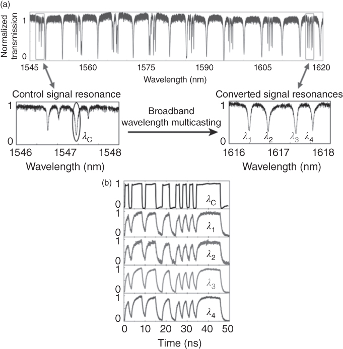
Figure 4 Wavelength multicasting using the coupled design of Fig. 1(d): (a) broadband transmission spectrum of the device and detail of the resonances used for the conversion of a signal at 1548 nm to four adjacent channels separated by 50 GHz and centered around 1617 nm; (b) input λC and converted (λ1–4) waveforms for a PRBS signal with 1 mW of peak power at λC.10
4 Reconfigurable spectral control
In our previous discussion on the general spectral features of different photonic molecule designs, we presented their transmission spectra with respect to the degeneracy condition between embedded and outer rings. The transition between these two conditions can be easily achieved using an integrated microheater to shift the outer ring resonances, as illustrated in Fig. 5. As the outer ring resonance approaches the identical embedded rings resonances, a clear avoided crossing (anticrossing) is observed for all the designs, a typical feature of coupled systems.

Figure 5 Reconfigurable spectral control: evolution of the transmission spectrum of photonic molecules with (a) one, (b) two uncoupled, and (c) two coupled embedded microrings as the outer microring resonances are shifted using a microheater. Insets in upper panels show the fabricated devices and schematics highlighting the actuated microheater (black). Bottom panels show the transmission traces for selected heater powers indicated in the upper plots by (i) and (ii).
The control of the coupled modes around an anticrossing can be used to fine-tune the ER of resonances; see transmission traces in Fig. 5(a). Such ER tuning can be used to optimize the efficiency of power-dependent functionalities in passive integrated structures, such as parametric frequency comb generation.15 In addition to ER tuning, the spectral anticrossing can be used for local mode dispersion compensation.16 17
While Fig. 5 only shows the spectral evolution when the outer microring resonances are shifted, a variety of spectral shapes can also be obtained by actuating the microheaters of the embedded microrings.
5 Toward reconfigurable mode-splitting control
The dynamic control of individual microrings in a photonic molecule design enables novel spectral control capabilities not fully deployed thus far, such as the active control of mode-splitting in a passive monolithically integrated platform. Dynamical control of mode-splitting in monolithically integrated platforms is highly desirable but challenging.18 The traditional solution based on a tunable Mach–Zehnder interferometer as the coupling element between resonators19 20 works only partially, since it also affects the optical phase of the resonant mode itself. As a result, instead of splitting control with fixed resonance positions, illustrated schematically in Fig. 6 (a), the obtained splitting control comes with significant resonance shifts, as in Fig. 6(b).

Figure 6 Reconfigurable splitting control: (a) ideal control (no resonance shift) and (b) actual control using MZI couplers (significant resonance shift). (c) The proposed scheme consists of detuning one embedded ring with respect to the other to control the CW–CCW mode coupling in the system. (d) Experimental splitting control from 60 GHz (central splitting) down to a single notch resonance. The small resonance shift is only due to thermal crosstalk. Inset: Schematic of the device highlighting the actuated microheater (black).18
A splitting control mechanism with markedly suppressed resonance shifts has been recently demonstrated in our group exploiting photonic molecules.18 Using the design of Fig. 1(d), the detuning between the embedded rings is used to control the coupling between clockwise (CW) and counterclockwise (CCW) modes. Starting with all three rings degenerate, one of the embedded rings is detuned with respect to the other two rings by means of a microheater (see Fig. 6(c)). As the detuning between embedded rings increases, the CW–CCW coupling is reduced.
Particularly, for those modes that remain confined in the two unaffected rings, the CW–CCW coupling reduction occurs with no change in their resonance condition and thus no resonance shift. The experimental results of Fig. 6(d) confirm the principle of reconfigurable splitting control from 60 GHz (central splitting) down to a single notch resonance. A small resonance shift is observed, which is only due to thermal crosstalk effects.18 Such effects can be eliminated using distinct dispersion control mechanisms, such as carrier effects or electro-optic effects. In addition, these mechanisms would enable low-power, ultrafast splitting modulation.
6 Conclusion
In this chapter, we discussed some of the features that make photonic molecules such valuable tools in the quest for photonic circuits with flexible spectral response and enhanced performance. We presented some basic designs and discussed their spectral features, spatial mode distributions, and dynamic spectral control. A few examples illustrated the advantages of using photonic molecules to overcome the drawbacks of single resonant devices and to enable novel mechanisms of performance optimization and spectral control, such as extinction ratio tuning and reconfigurable mode-splitting control. Photonic molecules might enable further advances in sensing, optical signal processing, microwave photonics, and nonlinear nanophotonics.
Acknowledgments
This work was partially supported by CNPq, CAPES, CePOF (05/51689-2), FOTONICOM (08/57857-2), and FAPESP (2012/17765-7, 2014/04748-2).
References
- 1. V. M. N. Passaro, C. de Tullio, B. Troia, M. La Notte, G. Giannoccaro, and F. De Leonardis, “Recent advances in integrated photonic sensors,” Sensors (Switzerland) 12, 15558–15598 (2012).
- 2. S. Feng, T. Lei, H. Chen, H. Cai, X. Luo, and A. W. Poon, “Silicon photonics: From a microresonator perspective,” Laser Photonics Rev. 6, 145–177 (2012).
- 3. J. Vila-Planas, E. Fernández-Rosas, B. Ibarlucea, et al., “Cell analysis using a multiple internal reflection photonic lab-on-a-chip,” Nature Photonics 6, 1642–1655 (2011).
- 4. D. Marpaung, C. Roeloffzen, R. R. Heideman, A. Leinse, S. Sales, and J. J. Capmany, “Integrated microwave photonics,” Laser Photonics Rev. 7, 506–538 (2013).
- 5. B. Jalali and S. Fathpour, “Silicon photonics,” J. Lightwave Technol. 24, 4600–4615 (2006).
- 6. M. J. R. Heck, J. F. Bauters, M. L. Davenport, et al., “Hybrid silicon photonic integrated circuit technology,” IEEE J. Sel. Top. Quantum Electron. 19, article no. 6387568 (2013).
- 7. W. Bogaerts, P. De Heyn, T. Van Vaerenbergh, et al., “Silicon microring resonators,” Laser Photonics Rev. 6, 47–73 (2012).
- 8. S. V. Boriskina, “Photonic molecules and spectral engineering,” chapter in: I. Chremmos, O. Schwelb, and N. Uzunoglu, eds., Photonic Microresonator Research and Applications, New York: Springer, 2010, pp. 393–421.
- 9. L. A. M. Barea, F. Vallini, G. F. M. Rezende, and N. C. Frateschi, “Spectral engineering with CMOS compatible SOI photonic molecules,” IEEE Photonics J. 5, article no. 6657691 (2013).
- 10. M. C. M. M. Souza, L. A. M. Barea, F. Vallini, G. F. M. Rezende, G. S. Wiederhecker, and N. C. Frateschi, “Embedded coupled microrings with high-finesse and close-spaced resonances for optical signal processing,” Opt. Express 22, 10430–10438 (2014).
- 11. C. Schmidt, M. Liebsch, A. Klein, et al., “Near-field mapping of optical eigenstates in coupled disk microresonators,” Phys. Rev. A 85, 033827 (2012).
- 12. X. Zeng and M. A. Popovic, “Design of triply-resonant microphotonic parametric oscillators based on Kerr nonlinearity,” Opt. Express 22, 15837–15867 (2014).
- 13. L. A. M. Barea, F. Vallini, P. F. Jarschel, and N. C. Frateschi, “Silicon technology compatible photonic molecules for compact optical signal processing,” Appl. Phys. Lett. 103, 201102 (2013).
- 14. Q. Xu, V. R. Almeida, and M. Lipson, “Micrometer-scale all-optical wave-length converter on silicon,” Opt. Lett. 30, 2733–2735 (2005).
- 15. S. A. Miller, Y. Okawachi, S. Ramelow, et al., “Tunable frequency combs based on dual microring resonators,” Opt. Express 23, 21527–21540 (2015).
- 16. C. M. Gentry, X. Zeng, and M. A. Popovic, “Tunable coupled-mode dispersion compensation and its application to on-chip resonant four-wave mixing,” Opt. Lett. 39, 5689–5692 (2014).
- 17. X. Lu, S. Rogers, W. C. Jiang, and Q. Lin, “Selective engineering of cavity resonance for frequency matching in optical parametric processes,” Appl. Phys. Lett. 105, 151104 (2014).
- 18. M. C. M. M. Souza, G. F. M. Rezende, L. A. M. Barea, A. A. G. von Zuben, G. S. Wiederhecker, and N. C. Frateschi, “Spectral engineering with coupled microcavities: Active control of resonant mode-splitting,” Opt. Lett. 40, 3332–3335 (2015).
- 19. A. H. Atabaki, B. Momeni, A. Eftekhar, E. S. Hosseini, S. Yegnanarayanan, and A. Adibi, “Tuning of resonance-spacing in a traveling-wave resonator device,” Opt. Express 18, 9447–9455 (2010).
- 20. X. Sun, L. Zhou, J. Xie, Z. Zou, L. Lu, H. Zhu, X. Li, and J. Chen, “Investigation of coupling tuning in self-coupled optical waveguide resonators,” IEEE Photonics Technol. Lett. 25, 936–939 (2013).