
2.7
Gallium Nitride-Based Lateral and Vertical Nanowire Devices
Y.-W. Jo, D.-H. Son, K.-S. Im and J.-H. Lee
School of Electronics Engineering, Kyungpook National University, 80, Daehak-ro, Buk-gu, Daegu, South Korea
1 Introduction
GaN-based field-effect transistors (FETs) are widely used in power switching and amplifier applications due to the superior material properties of GaN, such as wide bandgap, high breakdown electric field, and high electron saturation velocity, which result in high current density and high breakdown voltage.1 2 However, GaN-based devices still suffer from challenges, such as surface and buffer-related trapping effects, that occasionally result in severe current collapse decrease and degradation of the off-state performances. While surface-related problems can be effectively addressed by appropriate surface treatment and passivation techniques,3–6 trapping in the buffer layer cannot be easily solved because the buffer layer usually contains many defects originating from the heteroepitaxial growth of the GaN layer. Recently, AlGaN-/GaN-based triple-gate fin-shaped field-effect transistors (fin-FETs) have demonstrated superior off-state performance and also suggested a possible avenue for reducing the buffer-related trapping effects.7–10 Even though the GaN-based gate-all-around (GAA) structure have not been realized with top-down approach thus far due to their complicated fabrication process, the GAA structure seems to exhibit greatly improved on- and off-state performances due to the enhanced gate controllability.11–14 Furthermore, the GAA structure should also be more effective in eliminating buffer layer trapping because the entire active region of the device is surrounded by the gate metal and completely separated from the underlying thick GaN buffer layer.
In this chapter, we report on the first fabrication and characterization of GaN-based lateral and vertical nanowire (NW) FETs by using top-down approach, where we combined conventional e-beam lithography and dry etching techniques with strong anisotropic tetramethyl ammonium hydroxide (TMAH) wet etching.
2 Crystallographic study of GaN nanowires using TMAH wet etching
Wet etching techniques play an important role in the semiconductor device fabrication process. Wet etching usually provides high etching selectivity that often offers an advantage in simplifying the fabrication process compared to the dry plasma etching. However, it is very difficult to etch the III-nitride semiconductors with the conventional wet solutions because these materials have strong chemical stability.15 A few chemical solutions, such as hydroxide-based solutions (e.g., NaOH or KOH) were investigated to the etching of the III-nitride semiconductors due to their ability to react with Ga atoms to form Ga2O3 layer. Vertical and narrow nanorod arrays were formed using a plasma dry etch followed by an anisotropic wet etch in hydroxide solution for the purpose of high efficiency light emitting diodes (LEDs).16 However, it is very rare to use NaOH or KOH solution as the GaN etchant in electronic device fabrication because it contains alkali metal ions that cause severe threshold voltage instability. On the other hand, TMAH does not suffer from the ion contamination and has been successfully utilized in GaN-based device fabrication.3 8–11 17 When the GaN layer is exposed to the TMAH solution, Ga-polar (0001) plane is hardly etched (near-zero etch rate), whereas N-face plane is easily etched with the highest rate. This is because the dangling bond density (DBD) of N-face facet or other planes is larger than that of the Ga-polar (0001) facet.16 18, 19
The GaN NW patterns along the ![]() and
and ![]() were then defined by e-beam lithography using a polymethyl methacrylate (PMMA) resist and followed by transformer-coupled plasma-reactive ion etching (TCP-RIE) using a BCl3/Cl2 gas mixture as shown in Fig. 1(a) and (b), respectively. The cross section of the initial etched GaN layer had a trapezoidal shape with sloped sidewall surfaces as shown in the left SEM image of Fig. 1(a) and the top SEM image of Fig. 1(b). After the dry etch, the NWs were etched in TMAH (5% solution at 90 °C) for 30 min. Due to its strong anisotropic etch characteristics, the etching proceeds only in the lateral directions but not in vertical direction along <0001>. Etching along
were then defined by e-beam lithography using a polymethyl methacrylate (PMMA) resist and followed by transformer-coupled plasma-reactive ion etching (TCP-RIE) using a BCl3/Cl2 gas mixture as shown in Fig. 1(a) and (b), respectively. The cross section of the initial etched GaN layer had a trapezoidal shape with sloped sidewall surfaces as shown in the left SEM image of Fig. 1(a) and the top SEM image of Fig. 1(b). After the dry etch, the NWs were etched in TMAH (5% solution at 90 °C) for 30 min. Due to its strong anisotropic etch characteristics, the etching proceeds only in the lateral directions but not in vertical direction along <0001>. Etching along ![]() direction makes the pattern narrower but still maintains the trapezoidal shape as shown in the right SEM image of Fig. 1(a). Etching along
direction makes the pattern narrower but still maintains the trapezoidal shape as shown in the right SEM image of Fig. 1(a). Etching along ![]() direction, on the other hand, changes the shape from a wide trapezoid with sloped angles to a narrow rectangle with very steep side-wall surfaces as shown in the bottom SEM image Fig. 1(b). Figure 2(b) and (c) shows the GaN crystal with wurtzite structure with
direction, on the other hand, changes the shape from a wide trapezoid with sloped angles to a narrow rectangle with very steep side-wall surfaces as shown in the bottom SEM image Fig. 1(b). Figure 2(b) and (c) shows the GaN crystal with wurtzite structure with ![]() and
and ![]() crystal planes, respectively. The
crystal planes, respectively. The ![]() crystal plane has 58.4° slope (Figs 1(a) and 2(b)). On the other hand, the
crystal plane has 58.4° slope (Figs 1(a) and 2(b)). On the other hand, the ![]() crystal plane consists of both Ga and N atoms with 90° angle from the (0001) plane (Fig. 1(b) and (c)). The reason for the difference of the exposed plane along the wafer direction is due to the different etching rate between along
crystal plane consists of both Ga and N atoms with 90° angle from the (0001) plane (Fig. 1(b) and (c)). The reason for the difference of the exposed plane along the wafer direction is due to the different etching rate between along ![]() and
and ![]() directions. When the rectangular GaN pattern is etched by dry etching, the (0001) planes at the inside and the outside of the pattern and sidewalls of
directions. When the rectangular GaN pattern is etched by dry etching, the (0001) planes at the inside and the outside of the pattern and sidewalls of ![]() facets are exposed. The
facets are exposed. The ![]() facets have higher DBD (16.0 nm−2) than the (0001) plane (11.4 nm−2), which results in a higher TMAH etch rate,18 19 so the TMAH-etched GaN layer has a hexagonal shape due to its wurtzite crystal structure. As shown in the schematic of Fig. 1(a), the pattern along
facets have higher DBD (16.0 nm−2) than the (0001) plane (11.4 nm−2), which results in a higher TMAH etch rate,18 19 so the TMAH-etched GaN layer has a hexagonal shape due to its wurtzite crystal structure. As shown in the schematic of Fig. 1(a), the pattern along ![]() direction consists of the bottom hexagonal (0001) plane and the sidewall
direction consists of the bottom hexagonal (0001) plane and the sidewall ![]() facets with the trapezoidal shape. On the other hand, along the
facets with the trapezoidal shape. On the other hand, along the ![]() direction as shown in the schematic of Fig. 1(b), the sloped sidewall is first etched with relatively fast rate and when the vertical
direction as shown in the schematic of Fig. 1(b), the sloped sidewall is first etched with relatively fast rate and when the vertical ![]() crystal plane is exposed, the etching slows because the DBD of
crystal plane is exposed, the etching slows because the DBD of ![]() plane (14.0 nm−2) is smaller than that of
plane (14.0 nm−2) is smaller than that of ![]() plane.18 19 Further etching widens the
plane.18 19 Further etching widens the ![]() plane along
plane along ![]() direction.
direction.

Figure 1 Schematic illustrations of the fin pattern directions and etching profile. SEM images of the fin test structure after TMAH etching along the (a)  and (b)
  .
.

Figure 2 GaN crystal structure with Ga-face polarity showing various crystal planes: (a) (0000) c-plane; (b)  r-plane; (c)
  a-plane; and (d)
  m-plane.
To form the vertical GaN NW structure, the plasma-enhanced chemical vapor deposition (PECVD) SiO2 mask was first patterned by e-beam lithography with width and pitch of 300 nm. Dry etching with TCP-RIE was performed to obtain the initial trapezoidal NWs with height of 300 nm as shown in Fig. 3(a). Anisotropic wet etching in TMAH solution (5% concentration at 80 °C) was then applied for 11 min to reduce the diameter of the nanowire. The TMAH solution etches the nanowire under the SiO2 mask layer only in the lateral direction but not in the vertical direction, which results in NWs with average diameter of 100 nm and very steep sidewalls as shown in Fig. 3(b). The initial vertical GaN nanowire structure has two different planes: top (0001) c-plane and semipolar ![]() planes formed at the sidewalls. The TMAH solution can selectively etch the
planes formed at the sidewalls. The TMAH solution can selectively etch the ![]() N-polar sidewalls while leaving the (0001) Ga-polar top surface unaffected. The
N-polar sidewalls while leaving the (0001) Ga-polar top surface unaffected. The ![]() N-polar facets of the GaN vertical nanowires were removed gradually accompanied with the exposure of the
N-polar facets of the GaN vertical nanowires were removed gradually accompanied with the exposure of the ![]() facets. This is because the DBD of
facets. This is because the DBD of ![]() facets (12.1 nm−2) is smaller than that of
facets (12.1 nm−2) is smaller than that of ![]() facets (16.0 nm−2).18 The GaN nanowire with
facets (16.0 nm−2).18 The GaN nanowire with ![]() facets has the nonpolar characteristics.20 The corresponding atomic models matched to these crystal planes are shown in Fig. 2(b) and (d), respectively.
facets has the nonpolar characteristics.20 The corresponding atomic models matched to these crystal planes are shown in Fig. 2(b) and (d), respectively.
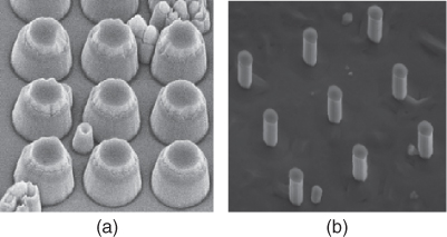
Figure 3 SEM images of GaN vertical NW structure after dry etching (a) and after subsequent TMAH wet etching for 11 min (b). The top SiO2 mask layer was deposited by PECVD.
3 Ω-shaped-gate lateral AlGaN/GaN FETs
To fabricate the AlGaN/GaN Ω-shaped-gate nanowire FET, the GaN epitaxial layers were first grown on c-plane sapphire substrate by MOCVD. The structure consisted of 30 nm-thick low temperature-grown GaN as a nucleation layer, 2 µm-thick undoped GaN semi-insulating layer in growth sequence, followed by an 80 nm-thick undoped GaN layer and 30 nm-thick Al0.3Ga0.7N layer. Hall effect measurements showed that the two-dimensional electron gas (2DEG) density and mobility were 9 × 1012 cm−2 and 1800 cm2/V·s, respectively.
Figure 4 shows the detailed fabrication process for the Ω-shaped GaN nanowire structure. The formation of nanowire structure was achieved by obtaining the ![]() crystal plane with very steep sidewall surface as described in Fig. 1. The initial patterns along the
crystal plane with very steep sidewall surface as described in Fig. 1. The initial patterns along the ![]() direction were defined by e-beam lithography using PMMA, followed by TCP-RIE using a BCl3/Cl2 gas mixture, which resulted in trapezoidal shape with sloped sidewalls as shown in Fig. 4(a). Then, TMAH wet etching (5% solution at 90 °C) was employed for 30 min to change from a wide trapezoid to a narrow rectangular shape with very steep sidewalls (see Fig. 4(b)). The 20 nm-thick atomic layer-deposited (ALD) HfO2 spacer mask for subsequent etching process was deposited on the steep sidewall surface as shown in Fig. 4(c). A second dry GaN etch step followed by TMAH lateral wet etching were used to etch the exposed GaN layer for 10 hours to form the Ω-shaped structure in Fig. 4(d) and (e). After removal of the sidewall HfO2 spacer, a 20 nm-thick ALD Al2O3 gate insulator and 30 nm-thick TiN gate metal were deposited (see Fig. 4(f)). Finally, Fig. 4(g) shows the cross-sectional TEM image for the GaN Ω-shaped nanowire structure. The total height and width of this structure were 280 and 55 nm, respectively. The width of the neck between the structure and the buffer layer was around 13 nm.
direction were defined by e-beam lithography using PMMA, followed by TCP-RIE using a BCl3/Cl2 gas mixture, which resulted in trapezoidal shape with sloped sidewalls as shown in Fig. 4(a). Then, TMAH wet etching (5% solution at 90 °C) was employed for 30 min to change from a wide trapezoid to a narrow rectangular shape with very steep sidewalls (see Fig. 4(b)). The 20 nm-thick atomic layer-deposited (ALD) HfO2 spacer mask for subsequent etching process was deposited on the steep sidewall surface as shown in Fig. 4(c). A second dry GaN etch step followed by TMAH lateral wet etching were used to etch the exposed GaN layer for 10 hours to form the Ω-shaped structure in Fig. 4(d) and (e). After removal of the sidewall HfO2 spacer, a 20 nm-thick ALD Al2O3 gate insulator and 30 nm-thick TiN gate metal were deposited (see Fig. 4(f)). Finally, Fig. 4(g) shows the cross-sectional TEM image for the GaN Ω-shaped nanowire structure. The total height and width of this structure were 280 and 55 nm, respectively. The width of the neck between the structure and the buffer layer was around 13 nm.

Figure 4 Process flow for GaN-based nanowire Ω-shaped FinFET: vertical (a) and narrow (b) fins structure after TMAH wet etching; (c) 20 nm-thick HfO2 layer deposition for sidewall spacer formation; fin structure after the second dry (d) and subsequent TMAH wet (e) etching; (f) final Ω-shaped device structure; (g) cross-sectional TEM images of Ω-shaped gate structure.
The GaN nanowire FET fabricated on this Ω-shaped structure exhibits much better performance than the reference device, with extremely low off-state leakage current as low as 10−10 mA, the subthreshold swing (SS) value of 59 mV/dec, and high ION/IOFF ratio (∼ 1010) as shown in the ID–VG curve of Fig. 5. On the other hand, the reference device had much higher off-state leakage current (10−7 mA), an SS of 74 mV/dec, and a lower ION/IOFF ratio ∼106. The difference in the off-state performance between two devices is because active region of the Ω-shaped structure is fully depleted and isolated from the thick GaN buffer region, comparing to the reference tri-gate structure.

Figure 5 Logarithmic (left) and linear (right) plots of drain current ID versus gate voltage VG in Ω-shaped device compare with reference trigate fin-FET.
4 Gate-all-around vertical GaN FETs
The epitaxial structure of Si-doped GaN/undoped-GaN/Si-doped GaN (70/120/500 nm) stack was grown by MOCVD on sapphire (0001) substrate. The doping densities of Si-doped and undoped GaN layers were 1.0 × 1019 cm−3 and 2.0 × 1016 cm−3, respectively. First, a SiO2 mask was patterned by e-beam lithography with both diameter and pitch of 300 nm. The vertical NW pillars were defined by TCP-RIE using a BCl3/Cl2 gas mixture, forming NWs with slanted sidewalls and height of 300 nm. The TMAH wet etch step (5% of solution at 80 °C) was used for 11 min to reduce the diameter of the nanowire as shown in Fig. 6(a), resulting in vertical sidewalls average NW diameter of 100 nm. The TMAH wet etching not only eliminates the plasma damage but also smoothens the etched GaN surface.17 Then, the SiO2 mask layer was removed prior to the deposition of a 10 nm-thick Al2O3 gate dielectric layer and a 20 nm-thick TiN gate metal by ALD. Then, a 20 nm-thick PECVD-deposited SiO2 mask layer and a photoresist (PR) were deposited, as shown in Fig. 6(b), followed by a blanket etch to remove the PR/SiO2/TiN/Al2O3 layers from the tops of the NWs as in Fig. 6(c). An SC-1 solution (NH4OH:H2O2:H2O = 1:1:5 at 70 °C) was used to define the TiN gate, with the SiO2 mask layer protecting the TiN from being etched in the lateral direction as shown in Fig. 6(d). For the isolation of gate from the drain, an additional 100 nm-thick SiO2 layer was deposited, followed by another blanket etch to enable the deposition of Ohmic Ti/Al contacts (Fig. 6(e)). After rapid thermal annealing at 500 °C for 30 s in N2 ambient, Ni/Au metal layers were deposited for gate pad (Fig. 6(d)).

Figure 6 Illustration of the device fabrication processes: (a) GaN vertical nanowire; (b) Al2O3/TiN/SiO2 deposition and PR spin coating; (c) blanket etching of PR and SiO2; (d) TiN/Al2O3 wet etching; (e) SiO2 deposition, PR spin coating, and PR/SiO2 dry etching; and (f) Ohmic contact formation.
Figure 7 shows a schematic and the cross-sectional TEM image of GaN-based vertical NW-FET. The number of nanowires in parallel is 12; the height of the TiN gate metal and the separation between the drain end of the gate metal and the drain are 200 and 100 nm, respectively.

Figure 7 Schematic (a) and cross-sectional TEM image (b) of the device.
Figure 8(a) exhibits the transfer curve at VD = 1 V of the fabricated GaN vertical NW-FET, which demonstrates a normally off operation with a threshold voltage of 0.6 V. The normalized maximum drain current and the maximum transconductance at VD = 1 V, divided by the total gate width (NW diameter multiplied by the number of NWs), are 130 mA/mm and 70 mS/mm, respectively. Figure 8(b) shows the subthreshold characteristics (at VD = 0.1 V) of device with SS of 153–163 mV/dec depending on the VG sweep direction, good ION/IOFF ratio as high as 109, and excellent off-state leakage current as low as ∼10−12 mA. We attribute the good off-state performance to GAA nanowire structure that eliminates the detrimental effects related to the buffer layer encountered in conventional planar-type FETs. Also, TMAH wet etching effectively smoothens and removes the plasma damage from the etched GaN surface.3

Figure 8 DC characteristics of the fabricated device: (a) transfer curve; (b) subthreshold characteristics with a double sweep of gate voltage.
5 Conclusion
To summarize, we have proposed and demonstrated GaN-based lateral and vertical nanowire FETs for the first time using top-down approach by combining conventional e-beam lithography and dry etching technique with strong anisotropic TMAH wet etching. The AlGaN-/GaN-based omega-gate NW FETs have been fabricated using TMAH orientation-selective lateral wet etching of ALD-deposited HfO2 sidewall spacer. The device exhibited excellent off-state performance: an SS of 62 mV/dec, close to the theoretical minimum, and an extremely low leakage current of 10−11 mA with a very high ION/IOFF ratio of 1010. We attribute these remarkable off-state characteristics to the Ω-shaped gate structure, which not only facilitates full depletion of the active region but also eliminates leakage paths between the active region and the thick GaN buffer layer. In addition, vertical GaN-based NW FETs with nanowire diameter of ∼100 nm were demonstrated by using top-down fabrication approach involving orientation-selective TMAH wet etching. The device exhibits very low off-state leakage current and high ION/IOFF ratio due to the GAA layout. The top-down approach provides a viable pathway toward GAA devices for III-nitride semiconductors, which are very promising candidates for steep-switching power device applications.
Acknowledgments
This work was supported by the BK21 Plus funded by the Ministry of Education (21A20131600011), the IT R&D program of MOTIE/KEIT (10048931), and the National Research Foundation of Korea (NRF) grant funded by the Korea Government (MSIP) (No. 2011-0016222, 2013R1A6A3A04057719).
References
- 1. T. P. Chow and R. Tyagi, “Wide bandgap compound semiconductors for superior high-voltage unipolar power devices,” IEEE Trans. Electron Devices 41, 1481–1483 (1994).
- 2. O. Aktas, Z. F. Fan, S. N. Fan, S. N. Mohammad, A. E. Botchkarev, and H. Morkoc, “High temperature characteristics of AlGaN/GaN modulation doped field-effect transistors,” Appl. Phys. Lett. 69, 3872–3874 (1996).
- 3. K.-W. Kim, S.-D. Jung, D.-S. Kim, et al., “Effects of TMAH treatment on device performance of normally off Al2O3/GaN MOSFET,”. IEEE Electron Device Lett. 32, 1376–1378 (2011).
- 4. K. Y. Park, H. I. Cho, H. C. Choi, et al., “Comparative study on AlGaN/GaN HFETs and MIS-HFETs,” J. Korean Phys. Soc. 45, S898–S901 (2004).
- 5. S. Arulkumaran, T. Egawa, H. Ishikawa, T. Jimbo, and Y. Sano, “Surface passivation effects on AlGaN/GaN high-electron-mobility transistors with SiO2, Si3N4, and silicon oxynitride,” Appl. Phys. Lett. 84, 613–616 (2004).
- 6. R. Vetury, N. Q. Zhang, S. Keller, and U. K. Mishra, “The impact of surface states on the DC and RF characteristics of AlGaN/GaN HFETs,” IEEE Trans. Electron Devices 48, 560–566 (2001).
- 7. B. Lu, E. Matioli, and T. Palacios, “Tri-gate normally-off power MISFET,” IEEE Electron Device Lett. 33, 360–362 (2012).
- 8. K.-S. Im, Y.-W. Jo, J.-H. Lee, S. Cristoloveanu, and J.-H. Lee, “Heterojunction-free GaN nanochannel FinFETs with high performance,” IEEE Electron Device Lett. 34, 381–383 (2013).
- 9. K.-S. Im, C.-H. Won, Y.-W. Jo, et al., “High-performance GaN-based nanochannel FinFETs with/without AlGaN/GaN heterostructure,” IEEE Trans. Electron Devices 60, 3012–3018 (2013).
- 10. K.-S. Im, R.-H. Kim, K.-W. Kim, et al., “Normally off single nanoribbon Al2O3/GaN MISFET,” IEEE Electron Device Lett. 34, 27–29 (2013).
- 11. K.-S. Im, V. Sindhuri, Y.-W. Jo, et al., “Fabrication of AlGaN/GaN Ω-shaped nanowire fin-shaped FETs by a top-down approach,” Appl. Phys. Express 8, 066501-1 (2015).
- 12. T. Bryllert, L.-E. Wernersson, L. E. Froberg, and L. Samuelson, “Vertical high-mobility wrap-gated InAs nanowire transistor,” IEEE Electron Device Lett. 27, 323 (2006).
- 13. K. Tomioka, M. Yoshimura, and T. Fukui, “A III–V nanowire channel on silicon for high-performance vertical transistors,” Nature 488, 189–192 (2012).
- 14. X. Zhao, J. Lin, C. Heidelberger, E. A. Fitzgerald, and J. A. del Alamo, “Vertical nanowire InGaAs MOSFETs fabricated by top-down approach,” Tech. Dig. IEDM (2013), pp. 28.4.1–28.4.4.
- 15. D. Zhuang and J. H. Edgar, “Wet etching of GaN, AlN, and SiC: A review,” Mater. Sci. Eng. Rep. 48, 1–46 (2005).
- 16. S.-Y. Bae, D.-J. Kong, J.-Y. Lee, D.-J. Seo, and D.-S. Lee, “Size-controlled InGaN/GaN nanorod array fabrication and optical characterization,” Opt. Express 21, 16854–16862 (2013).
- 17. Y.-W. Jo, D.-H. Son, C.-H. Won, K.-S. Im, J. H. Seo, I. M. Kang, and J.-H. Lee, “AlGaN/GaN finFET with extremely broad transconductance by side-wall wet etch,” IEEE Electron Device Lett. 36, 1008–1010 (2015).
- 18. W. Chen, J. Lin, G. Hu, et al., “GaN nanowire fabricated by selective wet-etching of GaN micro truncated-pyramid,” J. Crystal Growth 426, 168–172 (2015).
- 19. K. Hiramatsu, K. Nishiyama, A. Motogaito, H. Miyake, Y. Iyechika, and T. Maeda, “Recent progress in selective area growth and epitaxial lateral overgrowth of III-nitrides: Effects of reactor pressure in MOVPE growth,” Phys. Stat. Sol. 176, 535–543 (1999).
- 20. M. Kuroda, T. Ueda, and T. Tanaka, “Nonpolar AlGaN/GaN metal–insulator–semiconductor heterojunction field-effect transistors with a normally off operation,” IEEE Trans. Electron Devices 57, 368–372 (2010).