
3.3
Nanopower-Integrated Electronics for Energy Harvesting, Conversion, and Management
A. Romani, M. Dini, M. Filippi, M. Tartagni and E. Sangiorgi
Department of Electrical, Electronic, and Information Engineering “G. Marconi” and Advanced Research Center on Electronic Systems “E. De Castro”, University of Bologna, Via Venezia 52, 47521 Cesena FC, Italy
1 Introduction
The increasing interest on pervasive sensor networks and the steady development of electronic devices with low power consumption motivates the research on electronic systems capable of harvesting energy from the surrounding environment. Currently, most energy harvesters can provide in practical cases an output power density of about 10–100 μW/cm3.1 In this scenario, mechanical vibrations, thermal gradients, and photovoltaics represent the most promising power sources for supplying portable low-power electronic equipment.
For a successful application, it becomes essential to efficiently convert such low levels of input power. In this context, electronic interfaces based on recent commercial discrete components provide a cost-effective and easily implementable solution. Notable examples are reported in Refs 2–5, where intrinsic current consumptions down to 1 μA or less are achieved. However, in order to keep consumption low, discrete electronics must necessarily implement simplified, and thus less efficient, control schemes. In addition, nonnegligible, power-hungry parasitics are unavoidable when connecting discrete components.
The use of microelectronic technologies allows a series of circuit optimizations paving the way toward the exploitation of sub-microwatt power regimes, thanks to the significant reduction of parasitics and to the efficiency of custom-designed circuit topologies. As a direct consequence, the break-even in the power budget is achieved with smaller transducers or lower input power densities. This promises new applications that until recently have been stymied by the lack of power. Notable examples are reported in Refs 6–10, where several types of energy transducers providing up to a few microwatts are managed by fully custom-integrated circuits.
This chapter reviews some of the most promising integrated circuits (ICs) for power harvesting, conversion, and management, achieved either by industry or academia, intended for exploiting several different types of energy transducers. A specific case study consisting in a nanopower IC for harvesting power from multiple energy sources is also reviewed. The focus of the chapter is on the advantages conferred by nanoelectronic ICs in this specific field.
2 Commercial ICs for micropower harvesting
Many commercial ICs have been marketed over the years claiming to meet stringent energy-harvesting requirements. However, only very recently did commercial off-the-shelf components reach the ability of dealing with power sources providing input power down to few microwatts. Examples of recent IC implementations are chips such as the Texas Instruments bq2550411 and the STMicroelectronics SPV1050.12 Both ICs manage power sources down to few microwatts by implementing internal nanocurrent bias networks and by pursuing trade-offs between intrinsic power consumption and energy conversion efficiency. An ultralow intrinsic consumption is the key for the exploitation of the lowest possible input power densities. Both ICs perform maximum power point tracking (MPPT) by means of the fractional open circuit voltage (FOCV) technique, depicted in Fig. 1. This technique computes the maximum power point (MPP) as a fixed fraction of the open circuit voltage output by the energy transducer. This also means that power conversion is briefly stopped during the refresh of the MPPT. However, this technique offers negligible power consumption and a satisfactory trade-off with energy conversion efficiency. In the aforementioned ICs, the FOCV is in both cases obtained by means of resistive dividers. Large resistances reduce the consumed current but slow down the sampling time of the divided voltage. Another interesting feature of the above energy-harvesting ICs is the capability of performing a battery-less cold start-up. According to their datasheets, the bq25504 and SPV1050 chips can self-start, respectively, from 330 and 550 mV, with a minimum input power of few microwatts.
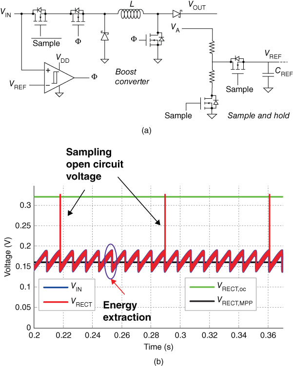
Figure 1 The FOCV MPPT technique: the basic circuit (a) and reference waveforms (b) during power conversion.
Excellent performance is also reported for the Cypress S6AE101A,13 which achieves super-low-power operation with an intrinsic consumption current of only 250 nA and a required start-up power of only 1.2 μW. According to the manufacturer, even the negligible levels of power obtained from compact solar cells under low-brightness environments of approximately 100 lm can be exploited. Unlike the previously mentioned ICs that implement inductor-based switching converters, the S6AE101A transfers power to an output capacitor using built-in switch control, by turning on a power switching circuit for as long as the capacitor voltage is within a preset maximum and minimum range. In case of low power levels, energy can be provided from connected primary batteries for auxiliary power. However, with respect to the previously mentioned ICs, this circuit requires a higher minimum input voltage in the order of 1 V.
Although the performance achieved by recent products is notable, there are still margins for improvement in terms of minimum required power and activation voltage. The following sections highlight recent achievements presented in scientific literature, with a special focus on nanopower-integrated solutions.
3 State-of-the-art integrated nanocurrent power converters for energy-harvesting applications
Many recently presented commercial integrated circuits claim to fulfill strict energy-harvesting requirements. However, intrinsic current consumptions on the order of microamperes or less have been reported only recently, largely in the scientific literature rather than commercial products – some recently published nanopower converters are collected in Table 1. These types of devices pave the way toward the exploitation of weaker power sources.
Table 1 A collection of recent nanopower energy-harvesting circuits
| Work | Type of sources | Features | Quiescent current/power | Minimum input power | Efficiency | Input voltage range |
| 45 | RF | MPPT with on–off time regulation | 181 nA | NA | <95% | 1.2–2.5 V |
| 21 | DC | Dynamic body bias, adaptive dead time | <0.5 μW | NA | 34%/72% at 0.18/0.45 V | >0.15 V |
| 7 | DC | FOCV MPPT, battery charger, cold start-up | 330 nA | 5 μW | 38%/>80% at 0.1/5 V | 0.08–3 V (330 mV start-up) |
| 46 | Thermoelectric | Variation-tolerant FOCV MPPT, no output voltage regulation, battery required | NA | NA | 72% | 70–600 mV |
| 6 | PV | On-chip PV cell, double-boost converter | NA | 1 μW | 65% | >0.5 V |
| 47 | PV | Reconfigurable circuit power and speed | 390 nW | NA | 90% | 0.9–2 V |
| 8 | Thermoelectric, PV, piezoelectric | Single shared inductor with asynchronous arbiter logic | 431 nA (9 sources) | 3 μW | 89.6% | <5.5 V (1.65 V start-up) |
| 18 | DC | Asynchronous control logic, fast battery-less start-up, nanopower LDO, active 223 mV start-up circuit | 121 nA | 935 nW | 77.1% | 0.074–2.5 V (223 mV start-up) |
| 44 | Piezoelectric | SECE with residual charge inversion, fast battery-less start-up | 160 nA | 300 nW | <85% | <5.5 V (1.65 V start-up) |
Optimized solutions based on discrete electronic components can reduce the intrinsic power consumption of energy-harvesting circuits. However, the practical baseline power limit of this type of circuits is in the order of tens of microwatts. To cite an example, a power management system for RF energy harvesting has been reported, based on an ultralow-power microcontroller unit (MCU) and an MPPT circuit built with on-chip peripherals.2 In Ref. 14, an FOCV MPPT technique was implemented with a similar configuration. However, even optimized MCU-based circuits typically consume about 10 μW, which poses a limit to the possible exploitable sources. Among the circuits with lower consumptions, a self-powered resonant DC/DC converter was reported with an input power lower than 4 μW by Adami et al.15
However, in order to operate in sub-microwatt regimes, the very low parasitics of circuits implemented in modern microelectronic processes can confer a significant advantage. In fact, several ICs reported in literature achieve even better performance, partly due to the implementation of nanopower techniques. A first example reported in Refs 7 16 is an integrated power management circuit consuming 330 nA with additional features such as battery charging and cold start-up from 300 mV. Similar power consumptions with the capability of managing multiple types of transducers are reported in Refs 8 17. An integrated DC/DC converter with a low dropout regulator (LDO) is reported to consume in standby about 520 nA,18 with the capability of battery-free self-starting at input voltages down to 200 mV. In these cases, the most frequently adopted technique is switching power conversion, and FOCV MPPT is assumed to be a good compromise between converted and consumed power. An alternative technique that exploits a buck switching converter with dynamic on–off time calibration and a regulated output voltage was reported to consume 217 nW.19 However, unlike boost converters, step-down topologies are not suitable for continuous energy storage, because the voltage on the output capacitor is limited. Inductor-less charge pumps20 with comparable intrinsic consumption and lower activation voltages down to 150 mV21 have also been proposed recently. In general, charge pumps have lower efficiencies than switching converters. Low-threshold MOSFETs allow to decrease the start-up voltage.22–24 The problem of activation voltage is particularly relevant in thermoelectric energy harvesting, where the voltage available is on the order of tens of millivolts. Lower input voltages have been exploited by implementing step-up oscillators.25–27
Among the viable energy transducers for supplying low-power electronic systems, piezoelectric transducers have been extensively studied, and a significant amount of recent scientific literature has focused on various aspects, from transducer physics to power conversion circuits. In the latter context, significant advantages have been introduced by synchronized switch harvesting techniques,28 that are typically based on the activation of LCR resonant circuits that are synchronized with vibrations. Because of the mainly capacitive output impedance of piezoelectric transducers, the peak voltage and the harvested power are usually increased. In addition, piezoelectric transducers limit converter intrinsic consumption because of very low activation rates and offer significant advantages because of their generally low oscillation frequencies, on the order of tens of Hz for macroscopic devices.
A well-known technique is the synchronized switch harvesting on inductor (SSHI),28 29 in which the transducer is connected to a rectifier bridge. The series connection of a switch and an inductor is connected in parallel to the transducer. When a peak-to-peak elongation ends, and the rectifier stops conducting, the switch is closed for a short time for inverting the polarity of voltage on the transducer. This inversion brings the transducer close to the opposite conduction threshold, so the next elongation starts from this favorable offset. The main consequence is that the rectifier, in an ideal case, is always conducting, and charge is continuously transferred to the output. However, since electrical charge is still transferred through the rectifier, the efficiency of the energy transfer depends on the operating point, and can be adversely impacted by very low or very high load currents. This drawback is not present in the synchronous electrical charge extraction (SECE) technique.5 30–34 In SECE, which is depicted in Fig. 2, the transducer is left in an open circuit state for most of the time. Only on voltage peaks, a series of switches connects the piezoelectric transducer to an inductor, so that charge is removed and the corresponding energy is stored in the magnetic field of the inductor. When the transducer is fully discharged, the inductor current has reached its maximum value. At that exact moment, switches between the transducer and inductor open, just as a new set of switches connects the charged inductor to a storage capacitor. The current decreases and in a way similar to a boost converter, as shown in Fig. 2. The SECE technique can also be implemented with a flyback topology,3 35 in order to reduce losses on freewheeling diodes. However, longer transients occur, and this increases energy losses, especially in case of large capacitive loads. It is worth to mention that the efficiency of SECE does not depend on the output bias, and that removing electrical charge on voltage peaks doubles the peak voltage. Besides this, SSHI36 and other synchronized-switch harvesters based on multistage converters or transformers, such as DSSH37 or SSHI-MR38 have also been reported to provide a better performance.

Figure 2 The SECE technique: a basic circuit showing current flow and reference waveforms during power conversion.
In this type of interface, one of the main limiting factors in micropower scenarios is the use of diodes in circuit implementations.28 39, 40 In general, the voltage drop across diodes wastes significant amounts of power. Negative voltage converters, based on a cross-coupled MOSFET bridge, represent a better solution for rectifying voltages while permitting bidirectional current flow.41 Active rectifiers42 43 also provide efficient performance at the cost of higher intrinsic power consumption, as do digitally controlled switches.8 31 A nanopower-integrated circuit implementing SECE and able to exploit the residual charge left on the transducer before the rectifier, leading to a more favorable voltage offset is reported in Ref. 44.
4 A multisource-integrated energy-harvesting circuit
As a case study, this section presents more insights into a nanocurrent IC able to convert and manage power from multiple and heterogeneous transducers.8 The IC employs a series of techniques that pursue a favorable trade-off between conversion efficiency and internal power consumption. Its operating principle is based on multichannel buck/boost conversion with a single shared inductor. Since a power converter is likely to operate in discontinuous current conduction mode when working with micropower transducers, the duty cycle of inductor utilization is expected to be very low. This is also true with SECE, where the duty cycle of activation is extremely low, due to the typically low oscillation frequencies of piezoelectric transducers. As a consequence, it is possible to serialize the accesses of multiple sources to the shared inductor by designing a specific arbiter circuit that manages MPPT and prevents concurrent accesses to the inductor.
The block diagram of the IC is shown in Fig. 3. It manages up to nine input channels for heterogeneous types of energy sources, namely, five piezoelectric and four DC sources. Two of the DC input ports are compatible with high voltage (HV) sources with 1 ≤ VDC0 ≤ 5 V, and two ports are optimized for low voltage (LV) sources, typically with 100 ≤ VDC0 ≤ 1 V. Such high number of input ports was included in the design for showing the degree of scalability of the technique and the still very low associated power consumption. Compatible transducers include piezoelectric devices, thermoelectric generators, rectennas, and photovoltaic cells. The converter core manages all the input channels and utilizes a single external inductor. The inductor value should be carefully determined, according to the associated switching speeds: values on the order of tens of microhenries require high switching rates with high consumption, whereas values in millihenries range require relatively large inductors and low switching rates.

Figure 3 Block diagram of the multisource energy-harvesting IC.8
A passive path through a depletion-mode MOSFET makes it possible to initially charge the storage capacitor. When the voltage stored on CST is sufficient to turn on the active circuits, the passive path is cut off by pulling low its gate signal. A 16 nA under voltage lockout circuit (UVLO in Fig. 3) manages this phase and enables active conversion as well.
When the system is fully self-powered and battery-less, the VDD input is connected to the output node VST, so that the converter supplies itself with the harvested energy, leading to a fully autonomous and self-powered solution. The core of the system is a fully asynchronous logic controller and arbiter that manage power conversion through the converter core from the individual sources. An FOCV MPPT is applied for DC sources, whereas piezoelectric sources are managed with an SECE circuit including local peak detection.
The IC has been designed in a 0.32 µm microelectronic process.
Figure 4 shows in more detail the circuits used for managing piezoelectric sources. The piezoelectric voltage is first rectified by a negative voltage converter with a MOSFET bridge for performing zero-voltage-drop rectification. When the IC operates in active mode, additional parallel-connected switches are used to fully discharge the piezoelectric source during the SECE cycle. The latter block is shown in the bottom part of Fig. 4 on the left. In order to issue piezoelectric conversion requests to the logic controller, a peak detector is implemented with a comparator. Since the circuit has no stable voltage supply, and the transducers have varying voltages, a specialized circuit block (denoted as HiPick in Fig. 4) was designed to select the highest available voltage to properly drive MOSFET switches. The nanopower comparator is shown at the top of Fig. 4 on the left, and has a nominal bias current of 16 nA. Comparators were frequently used in the design, and where fast response times were necessary, the bias current was dynamically increased only during critical phases of operation, for example, during single energy conversion cycles.

Figure 4 Detailed view of circuits for managing the piezoelectric transducers.8
The FOCV MPPT circuits are depicted in Fig. 5. Switched capacitors are used to set the FOCV at the 50% for linear sources and 75% for photovoltaic sources. Every eight conversion cycles, the MPP is refreshed by enabling the SAMPLE signal. An input buffer capacitor allows for continuous operation and low switching frequencies. During power conversion, a comparator with a dynamic 7× boost of bias current is used to maintain the source in the desired range around the MPP, with a hysteresis of ±28 mV.

Figure 5 The FOCV MPPT circuit for DC sources (a) and experimental voltage waveforms (b) acquired during chip operation.8
The power converter core is shown in Fig. 6. Conversion timing is controlled by means of zero-voltage switching (ZVS) and zero-current switching (ZCS) circuits. Also in this block, the comparators are dynamically biased with an increased current in the active phase in order to ensure zero idle static power and a fast ∼800 ns response of comparators during energy conversion. As a final design choice, the arbiter and the logic controller are implemented with asynchronous logic circuits. This spares the designers the need of generating and distributing clocks in the IC, with all the associated dynamic energy consumption.

Figure 6 The buck/boost converter core.8
The IC has a measured quiescent current of 360 nA with the VDD input biased at 3 V. The peak efficiency for piezoelectric input ports is 82%, while DC ports achieve up to 79%. Among the most important metrics, the energy consumed by the IC during a single energy transfer is very low, and was measured to be less than 2% of the energy input during a single conversion cycle with a 50 μW source. This low value indicates that the main energy losses are due to switch resistances rather than circuit consumption. The switches in the power converter could be made larger, but the current sizing was designed to keep the intrinsic consumption as low as possible. A top-view micrograph of the IC is shown in Fig. 7.
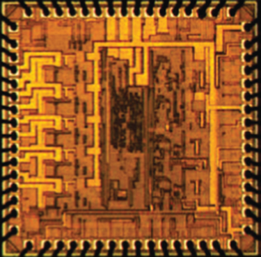
Figure 7 Micrograph of the IC. The total die area is 4.6 mm2.
5 Conclusion
Energy harvesting is an exciting field of research that is experiencing continuous progress. The increasing performance of energy transducers and the decreasing power requirements of power management ICs is bridging the gap toward the implementation of disruptive application. As a matter of fact, the microwatts barrier has already been broken, and current state-of-the-art ICs consume only a few hundred nanowatts. Such ultralow consumption allows power conversion and management circuits to achieve a positive power budget even when relying on weak power sources in harsh conditions. In this context, several commercial ICs for power management with excellent performance are available on the market. However, the potential of energy harvesting and of fully autonomous nodes is still far from being fully utilized. Shifting conventional design paradigms are encouraging designers to implement energy-aware techniques. A full energy optimization of all system components, including CPUs, sensors, and wireless interfaces, is expected to further contribute to the deployment of energy-autonomous nodes.
Acknowledgments
This work was supported in part by the European Community under the ENIAC Nanoelectronics Framework Program (Call ENIAC-2012-2, grant agreement Lab4MEMS no. 325622-2); by the 7th Framework Program (grant agreement NANOFUNCTION no. 257375); and by the Italian Ministry of Instruction, Research and University (MIUR), within the framework of the national project PRIN 2011 GRETA.
References
- 1. R. J. M. Vullers, R. Van Schaijk, I. Doms, C. Van Hoof, and R. Mertens, “Micropower energy harvesting,” Solid State Electron. 53, 684–693 (2009).
- 2. A. Dolgov, R. Zane, and Z. Popovic, “Power management system for online low power RF energy harvesting optimization,” IEEE Trans. Circ. Syst. I 57, 1802–1811 (2010).
- 3. T. Paing and R. Zane, “Design and optimization of an adaptive non-linear piezoelectric energy harvester,” Proc. 26th Annual IEEE Appl. Power Electronics Conf. (APEC) (2011), pp. 412–418.
- 4. S. Boisseau, P. Gasnier, M. Gallardo, and G. Despesse, “Self-starting power management circuits for piezoelectric and electret-based electrostatic mechanical energy harvesters,” J. Phys. Conf. Series 476, 012080 (2013).
- 5. A. Romani, M. Filippi, M. Dini, and M. Tartagni, “A sub-µA standby current synchronous electric charge extractor for piezoelectric energy harvesting,” ACM J. Emerg. Technol. Comput. Syst. 12, article no. 7 (2015).
- 6. E. Dallago, A. L. Barnabei, A. Liberale, P. Malcovati, and G. Venchi, “An interface circuit for low-voltage low-current energy harvesting systems,” IEEE Trans. Power Electron. 30, 1411–1420 (2015).
- 7. K. Kadirvel, Y. Ramadass, U. Lyles, et al., “A 330 nA energy-harvesting charger with battery management for solar and thermoelectric energy harvesting,” Tech. Dig. ISSCC (2012), pp. 106–108.
- 8. M. Dini, A. Romani, M. Filippi, V. Bottarel, G. Ricotti, and M. Tartagni, “A nanocurrent power management IC for multiple heterogeneous energy harvesting sources,” IEEE Trans. Power Electron. 30, 5665–5680 (2015).
- 9. E. E. Aktakka and K. Najafi, “A micro inertial energy harvesting platform with self-supplied power management circuit for autonomous wireless sensor nodes,” IEEE J. Solid-State Circ. 49, 2017–2029 (2014).
- 10. S. Bandyopadhyay, P. P. Mercier, A. C. Lysaght, K. M. Stankovic, and A. Chandrakasan, “23.2 A 1.1 nW energy harvesting system with 544 pW quiescent power for next-generation implants,” Tech. Dig. ISSCC (2014), pp. 396–397.
- 11. Texas Instruments, www.ti.com/product/bq25504 (accessed on Apr. 23, 2016).
- 12. STMicroelectronics, www.st.com/spv1050 (accessed on Apr. 23, 2016).
- 13. Cypress, www.spansion.com/downloads/S6AE101A_DS405-00026-E.pdf (accessed on Apr. 23, 2016).
- 14. A. Costanzo, A. Romani, D. Masotti, N. Arbizzani, and V. Rizzoli, “RF/baseband co-design of switching receivers for multiband microwave energy harvesting,” Sens. Actuators A 179, 158–168 (2012).
- 15. S.-E. Adami, V. Marian, N. Degrenne, C. Vollaire, B. Allard, and F. Costa, “Self-powered ultra-low power DC–DC converter for RF energy harvesting,” IEEE Faible Tension Faible Consommation (FTFC) Conf. (2012), pp. 1–4.
- 16. Y. Ramadass, “A 330 nA charger and battery management IC for solar and thermoelectric energy harvesting,” Presented at 3rd Intern. Workshop Power SoC (2012), paper 5.6.
- 17. S. Bandyopadhyay and A. Chandrakasan, “Platform architecture for solar, thermal, and vibration energy combining with MPPT and single inductor,” IEEE J. Solid-State Circ. 47, 2199–2215 (2012).
- 18. M. Dini, A. Romani, M. Filippi, and M. Tartagni, “A nano-current power management IC for low voltage energy harvesting,” IEEE Trans. Power Electron., 31, 4292–4304 (2015).
- 19. T.-C. Huang, C.-Y. Hsieh, Y.-Y. Yang, et al., “A battery-free 217 nW static control power buck converter for wireless RF energy harvesting with α-calibrated dynamic on/off time and adaptive phase lead control,” IEEE J. Solid-State Circ. 47, 852–862 (2012).
- 20. T. Tanzawa, “An optimum design for integrated switched-capacitor Dickson charge pump multipliers with area power balance,” IEEE Trans. Power Electron. 29, 534–538 (2014).
- 21. J. Kim, P. K. T. Mok, and C. Kim, “A 0.15 V input energy harvesting charge pump with dynamic body biasing and adaptive dead-time for efficiency improvement,” IEEE J. Solid-State Circ. 50, 414–425 (2015).
- 22. A. Richelli, S. Comensoli, and Z. M. Kovacs-Vajna, “A DC/DC boosting technique and power management for ultralow-voltage energy harvesting applications,” IEEE Trans. Ind. Electron. 59, 2701–2708 (2012).
- 23. G. Bassi, L. Colalongo, A. Richelli, and Z. M. Kovacs-Vajna, “A 150 mV–1.2 V fully-integrated DC–DC converter for thermal energy harvesting,” Proc. Intern. Symp. Power Electronics, Electrical Drives, Automation Motion (SPEEDAM) (2012), pp. 331–334.
- 24. L. Colalongo, Z. M. Kovacs-Vajna, A. Richelli, and G. Bassi, “100 mV–1.2 V fully-integrated DC–DC converters for thermal energy harvesting,” IET Power Electron. 6, 1151–1156 (2013).
- 25. A. Richelli, L. Colalongo, and Z. M. Kovacs-Vajna, “A 30 mV–2.5 V DC/DC converter for energy harvesting,” J. Low Power Electron. 11, 190–195 (2015).
- 26. E. Macrelli, A. Romani, R. P. Paganelli, A. Camarda, and M. Tartagni, “Design of low-voltage integrated step-up oscillators with microtransformers for energy harvesting applications,” IEEE Trans. Circ. Syst. I 62, 1747–1756 (2015).
- 27. A. Camarda, A. Romani, E. Macrelli, and M. Tartagni, “A 32 mV/69 mV input voltage booster based on a piezoelectric transformer for energy harvesting applications,” Sens. Actuators A 232, 341–352 (2015).
- 28. E. Lefeuvre, A. Badel, C. Richard, L. Petit, and D. Guyomar, “A comparison between several vibration-powered piezoelectric generators for standalone systems,” Sens. Actuators A 126, 405–416 (2006).
- 29. Y. C. Shu, I. C. Lien, and W.-J. Wu, “An improved analysis of the SSHI interface in piezoelectric energy harvesting,” Smart Mater. Struct. 16, 2253–2264 (2007).
- 30. A. Romani, M. Filippi, and M. Tartagni, “Micropower design of a fully autonomous energy harvesting circuit for arrays of piezoelectric transducers,” IEEE Trans. Power Electron. 29, 729–739 (2014).
- 31. A. Romani, C. Tamburini, A. Golfarelli, et al., “Dynamic switching conversion for piezoelectric energy harvesting systems,” Proc. IEEE Sensors Conf. (2008), pp. 689–692.
- 32. A. Romani, R. P. Paganelli, E. Sangiorgi, and M. Tartagni, “Joint modeling of piezoelectric transducers and power conversion circuits for energy harvesting applications,” IEEE Sens. J. 13, 916–925 (2013).
- 33. M. Dini, M. Filippi, M. Tartagni, and A. Romani, “A nano-power power management IC for piezoelectric energy harvesting applications,” Proc. 9th Conf. PhD Research Microelectronics Electronics (PRIME) (2013), pp. 269–272.
- 34. M. Dini, M. Filippi, A. Romani, V. Bottarel, G. Ricotti, and M. Tartagni, “A nano-power energy harvesting IC for arrays of piezoelectric transducers,” Proc. SPIE 8763, 87631O (2013).
- 35. P. Gasnier, J. Willemin, S. Boisseau, et al., “An autonomous piezoelectric energy harvesting IC based on a synchronous multi-shot technique,” IEEE J. Solid-State Circ. 49, 1561–1570 (2014).
- 36. D. Guyomar, A. Badel, E. Lefeuvre, and C. Richard, “Toward energy harvesting using active materials and conversion improvement by nonlinear processing,” IEEE Trans. Ultrason. Ferroelectr. Freq. Control 52, 584–594 (2005).
- 37. M. Lallart, L. Garbuio, L. Petit, C. Richard, and D. Guyomar, “Double synchronized switch harvesting (DSSH): A new energy harvesting scheme for efficient energy extraction,” IEEE Trans. Ultrason. Ferroelectr. Freq. Control 55, 2119–2130 (2008).
- 38. L. Garbuio, M. Lallart, D. Guyomar, C. Richard, and D. Audigier, “Mechanical energy harvester with ultralow threshold rectification based on SSHI nonlinear technique,” IEEE Trans. Ind. Electron. 56, 1048–1056 (2009).
- 39. Y. Ramadass and A. Chandrakasan, “An efficient piezoelectric energy harvesting interface circuit using a bias-flip rectifier and shared inductor,” IEEE J. Solid-State Circ. 45, 189–204 (2012).
- 40. N. Krihely and S. Ben-Yaakov, “Self-contained resonant rectifier for piezoelectric sources under variable mechanical excitation,” IEEE Trans. Power Electron. 26, 612–621 (2011).
- 41. C. Peters, J. Handwerker, D. Maurath, and Y. Manoli, “An ultra-low-voltage active rectifier for energy harvesting applications,” IEEE Intern. Symp. Circ. Syst.(ISCAS) (2010), pp. 889–892.
- 42. C. Peters, J. Handwerker, D. Maurath, and Y. Manoli, “A sub-500 mV highly efficient active rectifier for energy harvesting applications,” IEEE Trans. Circ. Syst. I 58, 1542–1550 (2011).
- 43. Y. Sun, N. H. Hieu, C.-J. Jeong, and S.-G. Lee, “An integrated high-performance active rectifier for piezoelectric vibration energy harvesting systems,” IEEE Trans. Power Electron. 27, 623–627 (2012).
- 44. M. Dini, A. Romani, M. Filippi, and M. Tartagni, “A nanopower synchronous charge extractor IC for low-voltage piezoelectric energy harvesting with residual charge inversion,” IEEE Trans. Power Electron. 31, 1263–1274 (2016).
- 45. T. Huang, C. Hsieh, Y. Yang, et al., “A battery-free 217 nW static control power buck converter for wireless RF energy harvesting with calibrated dynamic on/off time and adaptive phase lead control,” IEEE J. Solid-State Circ. 47, 852–862 (2012).
- 46. J. Kim and C. Kim, “A DC–DC boost converter with variation-tolerant MPPT technique and efficient ZCS circuit for thermoelectric energy harvesting applications,” IEEE Trans. Power Electron. 28, 3827–3833 (2013).
- 47. N. K. Pour, F. Krummenacher, and M. Kayal, “A reconfigurable micro power solar energy harvester for ultra-low power autonomous microsystems,” in IEEE Intern. Symp. Circ. Syst. (ISCAS) (2013), pp. 33–36.