
3.4
Will Composite Nanomaterials Replace Piezoelectric Thin Films for Energy Transduction Applications?
R. Tao, G. Ardila, R. Hinchet, A. Michard, L. Montès and M. Mouis
IMEP-LAHC/Minatec, CNRS-Grenoble INP, UJF, 38016 Grenoble, France
1 Introduction
The piezoelectric effect is the conversion of mechanical strain into electrical energy (direct effect) or, conversely, the production of mechanical deformation by an input electric field (converse effect). It is widely used in applications such as lighters, speakers, medical ultrasound transducers, precise positioning systems, and many others, using mainly bulk materials.1 At a smaller scale, piezoelectric thin films are used in applications ranging from MEMS/NEMS actuators to resonators.2 Other applications include mechanical sensors and energy harvesters used typically for wireless sensor networks (WSNs), with the objective of monitoring human health, environment, or structures such as airplanes or buildings.3 The integration of energy harvesters in WSN systems, in particular, helps to develop battery-less autonomous systems or, in other cases, eliminate complex wiring.
The most used piezoelectric materials in these applications are PZT and AlN thin films.2 At the nanoscale, ZnO and GaN in the shape of nanowires (NWs) are the most studied materials because they are relatively easy to fabricate4 and because of their enhanced electromechanical properties: higher flexibility and higher piezoelectric coefficients compared to their thin film counterparts.5
Piezoelectric NWs exhibit the so-called piezotronic effect,6 comprised of the coupling between piezoelectric and semiconducting properties, which can be used for such applications as mechanical sensors,7 8 transistors,6 programmable memories,9 optoelectronic devices,10 and chemical sensors.11 Further, such NWs can be integrated with insulators to create composite materials.12 13
After a brief review of thin film piezoelectric materials, their fabrication techniques, and typical applications, we present the experimental and theoretical study on individual piezoelectric NWs, with a focus on ZnO and GaN, and their particular properties. Then, we discuss the integration of such nanowires into composite materials for sensing and energy-harvesting applications, including a theoretical study on the improvement of their performance.
2 Thin film piezoelectric materials and applications
Usually, MEMS devices utilizing piezoelectric materials exploit two particular response modes, which are identified by subscripts (33 and 31) indicating the axis of the applied field and the produced strain or stress.14 These are associated with piezoelectric coefficients relating the electric field and the strain (d) or the stress (e). For instance d31 relates the in-plane strain to the out-of-plane electric field and d33 relates the out-of-plane strain to the electric field in the same direction.
Other than the piezoelectric coefficients, it is often useful to consider the energy conversion efficiency defined by the expression:

where subscripts i and j represent the relative directions, ![]() 0 is the permittivity of free space,
0 is the permittivity of free space, ![]() r is the relative dielectric constant, and sij is the compliance or the inverse of the stiffness. This expression shows that in addition to large piezoelectric coefficients, it is also important to have a large stiffness and low dielectric constant. Thus, materials with high piezoelectric coefficients are very useful in actuation applications, but materials with high conversion efficiencies are also of interest for sensing and energy harvesting, even if they do not have large piezoelectric coefficients.15
r is the relative dielectric constant, and sij is the compliance or the inverse of the stiffness. This expression shows that in addition to large piezoelectric coefficients, it is also important to have a large stiffness and low dielectric constant. Thus, materials with high piezoelectric coefficients are very useful in actuation applications, but materials with high conversion efficiencies are also of interest for sensing and energy harvesting, even if they do not have large piezoelectric coefficients.15
In order to exploit the piezoelectric effect, typical MEMS applications use piezoelectric materials integrated into bendable structures such as beams, bridges, or membranes. Many applications can be cited using such structures: mirror arrays for video projection, microphones, RF resonators, and filters for mobile applications, accelerometers and ink-jet printing heads.
The applicability of piezoelectric materials in emerging fields depend on several factors:1 (i) the ability to deposit piezoelectric materials at low temperatures to ensure compatibility with CMOS technologies or polymers; (ii) the ability to integrate them into non-Si substrates, such as metal foils and polymers; and (iii) the ability to deposit piezoelectric materials over topologies for 3D sensors or actuators.
• Thin film piezoelectric materials
At the MEMS scale, many piezoelectric materials have been studied and successfully integrated: compound semiconductors such as nitrides like AlN or oxides like ZnO, ferroelectrics such as Pb(ZrxTi1−x)O3 (PZT), and polymers such as polyvinylidene fluoride (PVDF).16 In the case of polycrystalline ferroelectrics, poling at a certain temperature (100–200 °C) is needed to reorient the polar axis, in which case the piezoelectric effect is averaged over all the grains of the layer, reducing the piezoelectric properties compared to perfectly aligned domains. This is not the case in nonferroelectric materials such as ZnO, GaN, or AlN, where the fabrication process provides the alignment of the polar directions.17 This is an advantage in the case of 1D structures such as NWs, which are usually highly crystalline.6
The thin film materials with the best piezoelectric properties are ferroelectric such as PZT and very recently PMN-PT, which could present piezoelectric properties about 5–10 times those of PZT, but only if very specific conditions are satisfied in the deposition process.18 On the other hand, materials with lower piezoelectric properties such as AlN, ZnO, or GaN are also very attractive for their lower dielectric constants, which increase the energy conversion efficiency, as in Eq. (1).
Several techniques can be used to deposit thin film piezoelectric materials. Lead-based materials such as PZT can be deposited using metal-organic chemical vapor deposition (MOCVD), sputtering and chemical solution deposition, including sol–gel techniques.17 Thicknesses below 2 µm can typically be achieved while preserving high piezoelectric properties.19 In the case of PMN-PT, it can be deposited by sputtering, achieving thicknesses below 4 µm. These fabrication techniques usually require high temperature (∼650–750 °C) that may not be compatible with some applications, such as CMOS with Al metallization that cannot withstand temperatures above 400 °C. Some exceptions can be cited where hydrothermal methods (<200 °C) have been used to deposit thin layers (<500 nm) of PZT,20 although repeated processing must be used to reach a thickness of several tens of micrometers and the performance is inferior to bulk materials.1 On the other hand, AlN and ZnO thin films (<1 µm) are typically deposited by low-temperature sputtering (<400 °C), simplifying integration and compatibility with CMOS technologies, but the piezoelectric properties of such films are low compared to PZT.14 Finally, PVDF has higher piezoelectric properties than nonferroelectric materials, but its lower stiffness results in lower energy conversion efficiency.21
Fabricating composite materials using piezoelectric NWs could be a way to improve their performance, as well as compatibility with multiple substrates and CMOS technologies. Nanowires with 50 µm length have been reported,22 meaning that composite materials can be designed without thickness restrictions.
3 Individual ZnO and GaN piezoelectric nanowires: experiments and simulations
Semiconducting piezoelectric NWs, such as ZnO and GaN, have been investigated due to their high piezoelectric coefficients and mature growth methods.23 Many modeling and experimental approaches have been considered to characterize their mechanical, electrical, and electromechanical properties.
• Mechanical properties of ZnO and GaN piezoelectric NWs
Molecular dynamic (MD) modeling24 and finite element method (FEM)25 have been used to determine the mechanical properties of ZnO and GaN NWs. At the same time, different loading modes, including tension, compression, and bending, are applied to the NW using MEMS, in situ SEM/TEM, AFM, cantilever in situ SEM/TEM, and other experimental techniques, in order to obtain experimental mechanical properties.
Agrawal et al. studied the elasticity size effects in ZnO NWs,26 where they calculated Young's modulus of NWs with diameters ranging from 5 to 20 nm by first principle methods. Results showed that as the diameter decreased, Young's modulus increased from 169 to 194 GPa, which was consistent with the size effect reported by Chen et al.27 They also measured ZnO NWs with diameters ranging from 20.4 to 412.9 nm by applying a uniaxial tensile load inside a TEM. Young's modulus was found to increase rapidly as the diameter went below 80 nm. Bernal et al. characterized experimentally c- and a-axes of GaN NWs using a MEMS-based in situ TEM uniaxial testing technique.24 Unlike ZnO NWs, GaN NWs with diameters larger than 30–40 nm presented an elastic modulus similar to bulk values. However, due to the uncertainties of boundary conditions, surface status, and calibration deviation of different methods, the mechanical characterization results in literature exhibit significant scatter for both ZnO and GaN NWs.
• Electrical properties of ZnO and GaN piezoelectric NWs
Yang et al. reported measurements of the dielectric constant of single pencil-like ZnO nanowires using the scanning conductance microscopy (SCM) technique.28 Their results showed that the dielectric constant of ZnO NWs had significant size dependence within the experimental manipulation range, and it was much smaller than bulk value (see Fig. 1).

Figure 1 Diameter dependence of the dielectric constant in a single pencil-like ZnO NW.
(Source: Yang et al.28 Reproduced with permission of the American Chemical Society).
• Piezoelectricity study of ZnO and GaN piezoelectric NWs
Piezoelectricity is a linear electromechanical coupling, which manifests the interconversion between electric and mechanical energy. Piezoelectric constants of piezoelectric NWs are commonly measured by applying tensile loading or lateral bending of the material with simultaneous measurement of generated charge or electric potential. For example, Minary-Jolandan et al. presented a method based on scanning probe microscopy (SPM) to probe the 3D piezoelectric matrix of individual piezoelectric NWs.29
Since the experimental characterization of the coupling properties still faces challenges, such as the manipulation of individual NWs, the contact resistance between the sample and the measurement tools, and the sensitivity of output electrical signals, computational simulations can also contribute to the understanding of this effect. Thus, from first principles calculations, Xiang et al. demonstrated that piezoelectric constants of ZnO NWs increase monotonically as the radius decreases.30 This size dependence effect was studied later in both ZnO and GaN NWs with radius ranging from 0.6 to 2.4 nm by Espinosa and coworkers.31 They reported that GaN NWs manifest a greater size dependence than ZnO NWs and that their piezoelectric constants can be improved by two orders of magnitude compared to the bulk values if the NW diameter can be reduced to under 1 nm.
The piezoelectric behavior of individual NWs was also investigated by FEM simulations. Wang and coworkers first proposed a continuum model for simulating the electrostatic potential in a laterally bent ZnO NW with 50 nm diameter and 600 nm length.32 The voltage drop created across the cross section of the NW was around ±0.3 V when the bending force was 80 nN.
Initial simulations considered ZnO and GaN as insulators; however, they are semiconductors with a relatively wide bandgap. They are doped during the synthesis by defects and impurities, either intentionally for achieving certain functionality or through accidental doping due to the growth mechanism.33 Gao and Wang investigated the behavior of free charge carriers in a bent piezoelectric n-type ZnO NW under thermodynamic equilibrium conditions by inducing donors into the model.34 They demonstrated that the potential generated by NWs is screened by the charge carriers.
4 Piezoelectric composite materials using nanowires
Individual NWs provide typically very low power (∼1 pW).35 To increase the energy generated, NWs are usually integrated either laterally36 or vertically37 on the substrate to form piezoelectric composite materials. Considering large-scale fabrication and commercial application, vertically integrated nanogenerators (VINGs) including a composite piezoelectric layer appear to be an attractive option.
The VING structure was first introduced by Wang and his group37 to harvest bending mechanical energy. Initial VING designs employed ZnO NWs and were based on a five-layer flexible plate, illustrated in Fig. 2. Typically, VING composites are fabricated on Si wafers to work with compressive pressures13 or on flexible substrates such as metallic foil38 or even paper39 to work with bending forces.

Figure 2 Nanogenerator composed of a five-layer flexible plate with PMMA-surrounded ZnO NWs grown vertically on both sides of a polymer substrate and electrodes deposited on both top and bottom.
(Source: Hu et al.37 Adapted with permission of the American Chemical Society).
To study the performance of the VING structure, we have conducted computational simulations on ZnO NW-based nanocomposites in both compression and flexion modes. Matrix materials and ZnO properties were varied to compare with conventional thin film generators.
• VING working under compressive pressure
In compression mode, the core function part of the simplified model (named NG cell for nanogenerator cell) is one NW surrounded by matrix material, where the input pressure on the top surface is equal to the one on the entire structure (see Fig. 3). Symmetry boundary conditions are applied at the lateral surfaces on the assumption that identical NG cells surrounding the target one. In this case, the NW is immersed in PMMA, which protects it from the electrical leakage or short circuits. Then, top and bottom surfaces are defined as electrodes to harvest the generated electrostatic energy. When the device is compressed, part of the input mechanical energy is stored inside the core piezoelectric NW, and then it is converted into electric energy through direct piezoelectric effect. Finally, the electric energy is driven out by the external circuit (not shown).

Figure 3 Scheme of a composite piezoelectric material on a metallic substrate (a) and the NG cell in compression mode (b).38
The compressive pressure is considered to be a constant (1 MPa). The initial cell size is 100 × 100 × 700 nm, with NW radius r = 25 nm, and length L = 600 nm. The size is varied by changing the NW diameter/cell width ratio, representing the density of the NWs. The electrical and piezoelectric properties of ZnO are varied respectively to study their influence. As mentioned above, the mechanical properties are not known with great certainty, so we do not consider the variation of ZnO elastic moduli in the current simulations.
Figure 4(a) shows the absolute value of the output potential varying with the previously defined ratio. The thin film model generates ∼10 mV. When the model of the composite NG cell is considered, the potential increases by a factor of 8 (at ratio = 0.4) even though the NW is assumed to have the same properties as a thin film.40–42 The enhancement is due to the soft PMMA matrix, which concentrates the strain inside ZnO. Besides, because of the 3D dielectric losses and the deviation of the strain field around the NWs, a smaller size ratio improves the storage of mechanical energy but reduces the electrical energy stored.
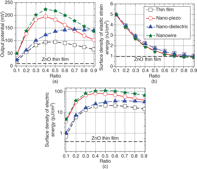
Figure 4 Absolute value of (a) output potential, (b) surface density of elastic strain energy, and (c) electric energy of NG cells working in compression mode using ZnO thin film properties, nano dielectric and piezoelectric constants, and NW properties, respectively. Results using a ZnO thin layer were calculated as reference.
In contrast, a high size ratio increases the capacity to store electrical energy in the NG, at the expense of reduced mechanical energy storage (see Fig. 4(b)). The trade-off of these effects forms a potential curve with a peak at ratio = 0.4. Since the dielectric constant decreases with the NW radius,28 the electric energy loss through the top insulating layer is smaller in NG cell.13 As the ratio increases, the dielectric constant becomes the major factor that influences the output potential. For the cell with nanoscale piezoelectric coefficients,8 the potential curve follows the trend of the thin film cell but increases by roughly a factor of 2. In summary, the potential of an NG cell with nanowire properties has been enhanced by 22 times compared to the thin film model and by ∼2.4 times compared to the NG cell with thin film properties. When we calculate the electric energy from the potential and the equivalent capacitance of this structure, we find the maximum shifts to higher NW density because of larger capacitance, as shown in Fig. 4(c).
• VING working under bending force
Similar to the compression case, the model only considers the unit cell at the central zone of the device (Fig. 5) with appropriate boundary conditions for fast FEM modeling. When the device is bent as a doubly clamped plate, the individual NW is in compression or extension (depending on the position of the NW on the plate) and is elongated or shortened in the c-axis direction.43 The input strain on the NG cell is calculated from a 2D model of the plate bent by a hydrostatic pressure (100 Pa) chosen to work in the linear mechanical regime.
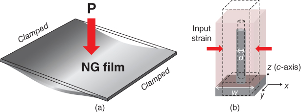
Figure 5 Schematic picture of NG membrane (a) and NG cell (b) in flexion mode.38
Figure 6(a) shows the output potential of the NG cell with thin film properties, which increases with the size ratio. But NG cells with nano properties show different behavior. An NG cell with only nano piezoelectric coefficients only generates a higher potential at a size ratio around 0.4. On the other hand, an NG cell with a nano dielectric constant manifests a monotonically increasing potential with size ratio. Since the nano dielectric constant of ZnO is smaller than PMMA, the electric energy loss decreases as the volume fraction occupied by ZnO increases – see Fig. 6(b). Combining these two nanoproperties, the NG cell shows a similar changing trend compared to a thin film cell but with an increase by a factor of 3.5.

Figure 6 Absolute value of (a) potential and (b) surface density of electric energy of NG cells working in flexion mode using ZnO thin film properties, nano dielectric constant, nano piezoelectric constant, and NW properties, respectively. Results using a thin ZnO layer were calculated as reference.
Although using nano properties improves the energy conversion and potential generation of VING in flexion mode, the performances are lower than ZnO thin film generators based on the simulation results. The performance of this composite material can be further improved by using different matrix materials. Figure 7 displays the simulation results of NG cells using PMMA, SiO2, Si3N4, and Al2O3 as matrix material, respectively, as well as the comparison with a ZnO thin film.

Figure 7 Absolute value of (a) potential, (b) surface density of elastic strain energy, and (c) surface density of electric energy of NG cells working in flexion mode using PMMA, SiO2, Si3N4, and Al2O3 as matrix material, respectively. Results using a thin ZnO layer were calculated as reference.
Given their higher rigidity, SiO2, Si3N4, or Al2O3 matrices enhance the input strain of the NG cell when the entire NG membrane is still bent by 100 Pa pressure (see Fig. 7(b)). Also, given their larger relative permittivity, they reduce the energy loss passing through the top insulating layer, as shown in Fig. 7(c). As a result, the potential generated is higher than a thin ZnO film starting from a ratio ∼0.3–0.5, and reaches a peak value that is 1.5–2.5 times larger than the reference ZnO thin film of Fig. 7(a). Since the improvement is largely due to the increase of input strain and the reduction of electric energy loss, potential and electric energy both increase with the size ratio.
• Effect on the alignment of the NWs
The models described in the preceding sections consider composite materials based on vertically aligned NWs. Although perfectly aligned NWs have been successfully fabricated,44 to the best of our knowledge all mechanical transducers reported to date have employed slightly inclined piezoelectric NWs.13 In this section, we evaluate the effect of the inclination of the NWs on the electric potential generated by a single cell.
The reference composite structure is formed by ZnO NWs (600 nm long) immersed on PMMA with a 100 nm-thick top insulating layer of Si3N4, which we previously found to be optimal compared to PMMA only. A single cell is evaluated including an increasing number of NWs having different inclination angles with respect to the ideal vertical case, starting from 1 NW up to 64 NWs. The FEM simulations take into account the fact that the NWs are grown along their c-axis, which is important to define the piezoelectric and mechanical properties; this has been done by defining these properties with respect to a rotated Cartesian axis aligned with each NW. All simulations in this section assume ZnO to have thin film piezoelectric properties.
Figure 8(a) shows the absolute value of the potential generated from the individual composite cell containing a single inclined NW as a function of its inclination. Simulations were carried out either taking into account the Cartesian axis rotation to correct the c-axis or without the axis rotation. When the inclination angle is small (below ∼5°), the curves are very close to each other and neglecting the c-axis correction does not produce appreciable error (maximum error of 2% below 5° and 8% below 12°). At higher inclination angles the error increases, reaching a maximum of ∼85%. An optimal inclination angle can also be observed when the inclination angle is close to 5°, increasing slightly the absolute electric potential at the top electrode. Then the potential is greatly reduced reaching a reduction of 50% for an inclination of ∼30°. A comparison of the results with and without c-axis correction for a specific angle is depicted in Fig 3.4.8(b) and (c).

Figure 8 FEM simulation results for a VING composite cell containing a single ZnO NW versus the inclination angle from the vertical, with and without c-axis correction: (a) absolute value of the piezoelectric potential generated; electric potential (mV) inside the cell with (b) and without (c) c-axis correction.
When two NWs are included in a single cell, several possibilities can be evaluated. To facilitate the study, we first considered an inclination in the xz-plane only. A series of simulations was conducted inclining only one of the two NWs, as shown in Fig. 9(a). The absolute value of the electric potential at the top electrode as a function of inclination is shown in Fig. 9(b). In general, the results are similar to the previews case with a single NW, with an optimal inclination close to 5°. This same behavior is observed if the inclination is taken to lie in the yz-plane (see Fig. 9(c)). The simulation results shows no clear trend when both NWs are inclined at small angles between 0° and 12° in the xz-plane. In some cases the electric potential is slightly increased (increase of ∼1%) compared to the ideal situation (∼69 mV), and in some cases the potential is markedly reduced (reduction of ∼17%).

Figure 9 FEM simulations of a single VING cell with two NWs under compression with inclination angles on the xz-plane: (a) displacement (nm) of one cell including one vertical NW and one NW inclined at ∼11°; (b) electric potential at the top electrode in function of the inclination angle of one NW; (c) displacement (nm) of one cell with one vertical NW and one NW inclined at ∼11° in the yz-plane.
In the case of four inclined NWs inside a cell, for different scenarios with inclination angles below 12° we observe a systematic reduction of the electric potential, ranging from 1% to 13% of the maximum. In order to verify this trend, cells including 36 and 64 ZnO NWs have been simulated at inclinations up to 12°, as shown in Fig. 10. The absolute value of the electric potential at the top electrode in both cases is close to 59 mV, representing a reduction of ∼14% from the ideal case. We expect that these simulations are closer to experimental reality because of the greater number of NWs in actual devices. Since the multi-NW simulations do not include c-axis correction, the results for the generated electric potential are likely underestimated by ∼8%.

Figure 10 FEM simulations results of the displacement (nm) of different single cells containing many NWs under compression with inclination angles below 12°. The absolute electric potential at the top electrode is presented for a single cell with (a) 36 and (b) 64 ZnO NWs.
These results show that the approach of considering a small number of NWs in a composite cell is only applicable if the NWs are truly vertical, providing the maximum electric potential. In the more realistic case of slightly inclined NWs, a large number of NWs is required in the cell to obtain consistent results. The integration of slightly inclined piezoelectric NWs can reduce the electric potential generated by as much of 14% compared perfectly vertical NWs.
5 Conclusion
Semiconducting piezoelectric NWs show significant potential for application in electronic and electromechanical sensors and energy harvesters. In particular, these nanostructures can be used to build composite piezoelectric materials (NWs in a dielectric matrix) that could offer several advantages when integrated vertically. First, NWs of various lengths (in particular, ZnO NWs up to several tens of micrometers long) have been reported, thus opening the possibility to fabricate composite layers thicker than standard thin films (<4 µm). Second, low-temperature fabrication process (<100 °C) make this technology compatible with CMOS devices and with different substrates, such as Si, polymers, plastics, metal foils, and even paper. Third, properties such as piezoelectricity, flexibility, and dielectric constant can be improved in NWs, thereby improving the performance of NW-containing composite materials. Finally, FEM simulations show that composites can provide better performance (more voltage or electric energy generated) compared to piezoelectric thin films of the same thickness, and that performance can be improved by operating in compression or flexion modes by the right choice of the dielectric matrix and NW density. On the other hand, some effects could reduce the performance of these composites: for instance the nonverticality of the integrated NWs and the screening by mobile charges or fixed ionized dopants.
Acknowledgments
This work has been partly supported by the French ministry (ANR COSCOF) and the regional research and development program NANO2017.
References
- 1. P. Muralt, R. G. Polcawich, and S. Trolier-McKinstry, “Piezoelectric thin films for sensors, actuators, and energy harvesting,” MRS Bull. 34, 658–664 (2009).
- 2. C.-B. Eom and S. Trolier-McKinstry, “Thin-film piezoelectric MEMS,” MRS Bull. 37, 1007–1017 (2012).
- 3. W. J. Choi, Y. Jeon, J.-H. Jeong, R. Sood, and S. G. Kim, “Energy harvesting MEMS device based on thin film piezoelectric cantilevers,” J. Electroceram. 17, 543–548 (2006).
- 4. Z. Guo, C. Andreazza-Vignolle, P. Andreazza, et al., “Tuning the growth of ZnO nanowires,” Phys. B: Condens. Matter 406, 2200–2205 (2011).
- 5. H. D. Espinosa, R. A. Bernal and M. Minary-Jolandan, “A review of mechanical and electromechanical properties of piezoelectric nanowires,” Adv. Mater. 24, 4656–4675 (2012).
- 6. X. Wen, W. Wu, C. Pan, Y. Hu, Q. Yang, Z. L. Wang, “Development and progress in piezotronics,” Nano Energy 14, 276–295 (2015).
- 7. Y. S. Zhou, R. Hinchet, Y. Yang, et al., “Nano-Newton transverse force sensor using a vertical GaN nanowire based on the piezotronic effect,” Adv. Mater. 25, 883–888 (2013).
- 8. R. Hinchet, J. Ferreira, J. Keraudy, et al., “Scaling rules of piezoelectric nanowires in view of sensor and energy harvester integration,” Tech. Dig. IEDM (2012), p. 6.2.1.
- 9. W. Wu and Z. L. Wang, “Piezotronic nanowire-based resistive switches as programmable electromechanical memories,” Nano Lett. 11, 2779–2785 (2011).
- 10. X. Wen, W. Wu, and Z. L. Wang, “Effective piezo-phototronic enhancement of solar cell performance by tuning material properties,” Nano Energy 2, 1093–1100 (2013).
- 11. R. M. Yu, C. F. Pan, J. Chen, G. Zhu, and Z. L. Wang, “Enhanced performance of a ZnO nanowire-based self-powered glucose sensor by piezotronic effect,” Adv. Funct. Mater. 23, 5868–5874 (2013).
- 12. S. Lee, R. Hinchet, Y. Lee, et al., “Ultrathin nanogenerators as self-powered/active skin sensors for tracking eye ball motion,” Adv. Funct. Mater. 24, 1163–1168 (2014).
- 13. R. Hinchet, S. Lee, G. Ardila, L. Montes, M. Mouis, Z. L. Wang, “Performance optimization of vertical nanowire-based piezoelectric nanogenerators,” Adv. Funct. Mater. 24, 971–977 (2014).
- 14. P. Muralt, “Piezoelectric thin films for MEMS,” Integr. Ferroelectr. 17, 297–307 (1997).
- 15. C. Baur, D. J. Apo, D. Maurya, S. Priya, and W. Voit, “Advances in piezoelectric polymer composites for vibrational energy harvesting,” chapter in: L. Li, W. Wong-Ng, and J. Sharp, eds., Polymer Composites for Energy Harvesting, Conversion, and Storage, Washington, DC: American Chemical Society, 2014, pp. 1–27.
- 16. K. A. Cook-Chennault, N. Thamby, and A. S. Sastry, “Powering MEMS portable devices – A review of non-regenerative and regenerative power supply systems with special emphasis on piezoelectric energy harvesting systems,” Smart Mater. Struct. 17, 043001 (2008).
- 17. P. Muralt, “Recent progress in materials issues for piezoelectric MEMS,” J. Am. Ceram. Soc. 91, 1385–1396 (2008).
- 18. S. H. Baek, M. S. Rzchowski, and V. A. Aksyuk, “Giant piezoelectricity in PMN-PT thin films: Beyond PZT,” MRS Bull. 37, 1022–1029 (2012).
- 19. D. Ambika, V. Kumar, K. Tomioka, and I. Kanno, “Deposition of PZT thin films with {001}, {110}, and {111} crystallographic orientations and their transverse piezoelectric characteristics,” Adv. Mater. Lett. 3, 102–106 (2012).
- 20. T. Morita, Y. Wagatsuma, Y. Cho, H. Morioka, H. Funakubo, and N. Setter, “Ferroelectric properties of an epitaxial lead zirconate titanate thin film deposited by a hydrothermal method below the Curie temperature,” Appl. Phys. Lett. 84, 5094–5096 (2004).
- 21. G. Ardila, R. Hinchet, M. Mouis, and L. Montès, “Scaling prospects in mechanical energy harvesting using piezoelectric nanostructures,” Dig. IEEE Intern. Semicond. Conf. Dresden-Grenoble (ISCDG) (2012), p. 75.
- 22. G. Zhu, R. Yang, S. Wang and Z. L. Wang, “Flexible high-output nanogenerator based on lateral ZnO nanowire array,” Nano Lett. 10, 3151–3155 (2010).
- 23. Y. W. Heo, D. P. Norton, L. C. Tien, et al., “ZnO nanowire growth and devices,” Mater. Sci. Eng. Rep. 47, 1–47 (2004).
- 24. R. A. Bernal, R. Agrawal, B. Peng, et al., “Effects of growth orientation and diameter on the elasticity of GaN nanowires,” Nano Lett. 11, 548–555 (2011).
- 25. A. Mitrushchenkov, G. Chambaud, J. Yvonnet, and Q.-C. He, “Towards an elastic model of wurtzite AlN nanowires,” Nanotechnology 21, 255702 (2010).
- 26. R. Agrawal, B. Peng, E. E. Gdoutos, and H. D. Espinosa, “Elasticity size effects in ZnO nanowires – A combined experimental–computational approach,” Nano Lett. 8, 3668–3674 (2008).
- 27. C. Chen, Y. Shi, Y. Zhang, J. Zhu, and Y. Yan, “Size dependence of Young's modulus in ZnO nanowires,” Phys. Rev. Lett. 96, 075505 (2006).
- 28. Y. Yang, W. Guo, X. Wang, Z. Wang, J. Qi, and Y. Zhang, “Size dependence of dielectric constant in a single pencil-like ZnO nanowire,” Nano Lett. 12, 1919–1922 (2012).
- 29. M. Minary-Jolandan, R. A. Bernal, I. Kuljanishvili, V. Parpoil, and H. D. Espinosa, “Individual GaN nanowires exhibit strong piezoelectricity in 3D,” Nano Lett. 12, 970–976 (2012).
- 30. H. J. Xiang, J. Yang, J. G. Hou, and Q. Zhu, “Piezoelectricity in ZnO nanowires: A first-principles study,” Appl. Phys. Lett. 89, 223111 (2006).
- 31. R. Agrawal and H. D. Espinosa, “Giant piezoelectric size effects in zinc oxide and gallium nitride nanowires. A first principles investigation,” Nano Lett. 11, 786–790 (2011).
- 32. Y. Gao and Z. L. Wang, “Electrostatic potential in a bent piezoelectric nanowire. The fundamental theory of nanogenerator and nanopiezotronics,” Nano Lett. 7, 2499–2505 (2007).
- 33. J. Gao, X. Zhang, Y. Sun, Q. Zhao, and D. Yu, “Compensation mechanism in N-doped ZnO nanowires,” Nanotechnology 21, 245703 (2010).
- 34. Y. Gao and Z. L. Wang, “Equilibrium potential of free charge carriers in a bent piezoelectric semiconductive nanowire,” Nano Lett. 9, 1103–1100 (2009).
- 35. C. Sun, J. Shi, and X. Wang, “Fundamental study of mechanical energy harvesting using piezoelectric nanostructures,” J. Appl. Phys. 108, 034309 (2010).
- 36. R. Yang, Y. Qin, C. Li, L. Dai, and Z. L. Wang, “Characteristics of output voltage and current of integrated nanogenerators,” Appl. Phys. Lett. 94, 022905 (2009).
- 37. Y. Hu, Y. Zhang, C. Xu, L. Lin, R. L. Snyder, and Z. L. Wang, “Self-powered system with wireless data transmission,” Nano Lett. 11, 2572–2577 (2011).
- 38. R. Tao, R. Hinchet, G. Ardila, L. Montès, M. Mouis, and A. D. Discription, “FEM modeling of vertically integrated nanogenerators in compression and flexion modes,” Proc. 10th Conf. PhD Research Microelectronics Electronics (PRIME), Grenoble (2014).
- 39. A. Manekkathodi, M.-Y. Lu, C. W. Wang, and L.-J. Chen, “Direct growth of aligned zinc oxide nanorods on paper substrates for low-cost flexible electronics,” Adv. Mater. 22, 4059–4063 (2010).
- 40. T. B. Bateman, “Elastic moduli of single crystal zinc oxide,” J. Appl. Phys. 33, 3309–3312 (1962).
- 41. G. Carlotti, G. Socino, A. Petri, and E. Verona, “Acoustic investigation of the elastic properties of ZnO films,” Appl. Phys. Lett. 51, 1889–1891 (1987).
- 42. N. Ashkenov, B. Mbenkum, C. Bundesmann, et al., “Infrared dielectric functions and phonon modes of high-quality ZnO films,” J. Appl. Phys. 93, 126–133 (2003).
- 43. R. Tao, R. Hinchet, G. Ardila, and M. Mouis, “Evaluation of vertical integrated nanogenerator performances in flexion,” J. Phys. Conf. Series 476, 012006 (2013).
- 44. V. Consonni, E. Sarigiannidou, E. Appert, et al., “Selective area growth of well-ordered ZnO nanowire arrays with controllable polarity,” ACS Nano 8, 4761–4770 (2014).