
Chapter 14
FluidFM: Development of the Instrument as well as Its Applications for 2D and 3D Lithography
Tomaso Zambelli1, Mathias J. Aebersold1, Pascal Behr1, Hana Han1, Luca Hirt1, Vincent Martinez1, Orane Guillaume-Gentil2 and János Vörös1
1ETH Zürich, Laboratory of Biosensors and Bioelectronics, D-ITET, CH-8092, Switzerland
2ETH Zürich, Institute of Microbiology, D-BIOL, CH-8093, Switzerland
Glass micropipettes were invented by Marshall Barber at the beginning of the twentieth century in his effort to fabricate a tool helping him with his experiments regarding bacterial isolation and inoculation [1, 2]. Because of their utility, cost-effectiveness, and straightforward fabrication protocols, glass pipettes have become a standard tool for single-cell manipulation. The technique can be used for numerous applications, not only in vitro but also in vivo: isolation of mammalian cells [3] and bacteria [4], transfection of mammalian cells [5, 6], local electroporation [7, 8], and, lastly, electrophysiological recording (patch clamp) of single cells [9–11]. Additionally, glass pipettes are also at the basis of a performing imaging and manipulation tool known as scanning ion conductance microscopy [12–14].
Glass pipettes are usually mounted on x–y–z micromanipulators relying on optical microscopy to control their positioning in the x–y plane and in the z direction (via image focusing). Due to the limits of resolution of standard optical microscopy (∼0.5 µm), contact between the glass pipette tip and the cell membrane cannot be reliably discriminated from penetration of the cell membrane by the pipette tip. This is an incertitude of the technique that often leads to fatal cell damage during experiments [15].
Different strategies have been explored to integrate glass pipettes with a force feedback for a controlled and thus gentle approach onto a cell (or more generally onto a surface): bent pipettes combined with a detection laser [16–18], piezoresistive sensor [19], and quartz tuning fork [20, 21].
At the end of 2006, we started envisioning a radically different solution based on atomic force microscopy (AFM [22]) and microchanneled AFM cantilevers (see next paragraph), which led to the development of the tool we called “fluidic force microscopy” (FluidFM) [23, 24].
This chapter is thought to recall the details of the instrumental development together with a presentation of the work on local surface modification and three-dimensional (3D) microprinting, whereas the following chapter by Guillaume-Gentil et al. deals with the work on single-cell manipulation. Hence, it is structured according to the following thread: microfabrication of microchanneled cantilevers, step-by-step development of the FluidFM, stiffness and flow calibration of the microchanneled cantilevers, and FluidFM for patterning.
14.1 Microchanneled AFM Cantilevers
14.1.1 Silicon-Based Hollow Probes
In the early 2000s, microfabrication of silicon-based AFM cantilevers with embedded microchannels was taken into consideration for the production of patterning devices at the nanoscale. In 2003, the first system pioneering the field was presented: the NAnoDISpensing tool (NADIS) [25]. Yet, the first NADIS version had no incorporated microchannel in the cantilever but only an opening at the apex of the hollow pyramidal tip, etched either by photolithography [25] or by focused ion beam (FIB) [26].
A year later, the first systems with an embedded microchannel connected to an open macro-reservoir were published [27]. As depicted in Figure 14.1, two main processes were formulated for the realization of such hollow silicon-based cantilevers: the “sacrificial layer” process and the “thermal bonding” process.
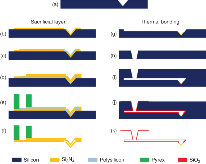
Figure 14.1 Simplified microfabrication processes for producing microchanneled silicon-based cantilevers with sacrificial layer (left column) and thermal bonding (right column) approaches.
Following the first approach, the microfountain pen from Deladi et al. [27] and the fountain nanoprobe from Espinosa and coworkers [28] were developed. The process [27] mostly consists of the following:
- A. KOH etching a single-crystal ⟨100⟩ silicon wafer to obtain the molds for the tips by anisotropic attack (54.7° angle of sidewalls with the surface)
- B. Deposition and patterning of a first Si3N4 layer with an outlet side hole for the cantilevers
- C. Deposition and patterning of a sacrificial polycrystalline silicon layer
- D. Deposition and patterning of a second Si3N4 layer for the cantilevers
- E. Patterning/dicing an additional Pyrex wafer and bonding of the two wafers for the reservoir
- F. Etching of the polycrystalline silicon for the channels and final release of the probes.
The reservoir could as well be directly etched and fabricated from the same wafer as the cantilever when the latter was designed in the opposite direction with the tip upward [28].
Based on the second approach (i.e., thermal bonding), other systems appeared in the subsequent years such as the Staufer's probe in 2005 (femto pipette [29]), the second version of NADIS in 2009 [30], or the Makino's one in 2010 (bioprobe [31]). The microfabrication strategy of this second approach consists of the following steps: (A) KOH etching a single-crystal ⟨100⟩ silicon wafer to obtain the molds for the tips by anisotropic attack (54.7° angle of sidewalls with the surface) with additional (G) etching for the channel and silicon nitride deposition at the tip level, (H) etching a second silicon wafer for the reservoir, (I) alignment and (J) bonding of the two wafers by thermal oxide growth at 1100 °C, and (K) release of the probes by etching away the remaining silicon wafer material.
For the development of the FluidFM, we first used microchanneled cantilevers according to [30]. As the technique was further refined, we switched to probes according to [27].
As shown in Figure 14.2, different tip designs were achieved such as flat or tubular tips as depicted in (b) [32] and pyramidal tips with apertures at the apex as shown in (e) or close to the apex as seen in (f). Cantilevers with apertures at the apex were fabricated on a wafer scale, taking advantage of the corned lithography concept [33], whereas apertures close to the apex were drilled individually by FIB. To photolithographically obtain nano-apertures directly at the apex, a sacrificial layer was conformably deposited on a V-groove template. Due to its higher effective thickness at the corner, the layer leaves a residue after etching. This residue can then be used as inversion mask or sacrificial material to free and open the cantilever at the apex.

Figure 14.2 SEM images of silicon nitride FluidFM probes. (a) Large view of a pyramidal cantilever. For mechanical stability the upper and lower layers of the probes are connected by two lines of pillars having a diameter of 3 µm each. (b) Tipless (i.e., without pyramid) probe with a 4 µm circular aperture. (c) FIB-cut cross section in correspondence of the microchannel. (d) FIB-cut cross section in correspondence of the hollow pyramid. (e) A 300 nm aperture at the apex obtained by photolithography and in (f) a 300 nm aperture close to the apex milled by FIB.
(Guillaume-Gentil et al. (2014) [24]. Copyright 2014. Reproduced with permission of Elsevier Inc.)
14.1.2 Polymer-Based Hollow Probes
First polymer-based standard (i.e., without embedded channel) cantilevers for AFM applications were fabricated using SU-8 in 1999 [34]. Since then, they have been used as stress sensors with integrated readout [35, 36]. Recently, SU-8 hollow cantilevers have been fabricated but without showing any fluidic and AFM capability [37].
SU-8 is an epoxy-based photoresist whose cationic polymerization is initiated by ultraviolet (UV) exposure and then completed by heat. As SU-8 has been standardly used in microfluidic applications, several processes have been developed to realize hollow structures made of SU-8/silicon [38], SU-8/PMMA [39], or SU-8/polydimethylsiloxane (PDMS) [40]. Nonetheless, it still is challenging to fabricate entire SU-8 fluidic devices made of patterned bottom and top channel layers since SU-8 is a negative-tone resist: oligomers in the bottom SU-8 layer of the microchannel must be still present in a sufficient amount to polymerize with those of top SU-8 layer in order to ensure a watertight sealing at the interface.
To fabricate SU-8 hollow cantilevers, several processes were investigated. Yet, for approaches based on embedded metal mask, lamination, partial exposure, or adhesive bonding proved to be not enough robust. A process based on an electrochemically deposited sacrificial copper layer was finally established, enabling the fabrication of functional probes with high sealing performance between the bottom and top layer [41]. The reason underlying the success of this process was the weak UV and heat exposure of the channel bottom layer (in yellow in Figure 14.3a) during the copper electroplating, so that free oligomers are still present (in the bottom layer), which can then extensively polymerize with those of the channel top layer (Figure 14.3f). To this end, a first SU-8 bottom layer was patterned on a substrate by defining the structures of the handling chip, cantilever, and circular aperture (Figure 14.3a). A copper conductive seed layer was then deposited by thermal evaporation at moderate temperature for low blackbody radiation (Figure 14.3b) before patterning a sacrificial AZ 4562 photoresist in orange used to confine the copper growth within the channel (Figure 14.3c). Next, a sacrificial copper layer was electroplated with the desired channel thickness (Figure 14.3d). The AZ photoresist was dissolved, followed by etching of the seed layer (Figure 14.3e). The devices were then patterned accordingly with the top SU-8 layer (Figure 14.3f) as well as the thick SU-8 layer for the chip handling (Figure 14.3g). Finally, the sacrificial copper inside the channels was removed in a copper etchant solution for several days before the final release of the probes (Figure 14.3h).

Figure 14.3 Microfabrication process of microchanneled SU-8 cantilevers on a wafer: (a) deposition of a Cr/Au/Cr release layer and patterning of a SU-8 bottom layer, (b) deposition of a copper seed layer, (c) patterning of a positive AZ sacrificial photoresist, (d) electroplating of a copper layer, (e) dissolution and etching of the positive photoresist and copper seed layer, (f) patterning of a SU-8 top layer, (g) patterning of a thick SU-8 chip layer for easy handling, and (h) etching of the channel sacrificial layer and final release from the wafer.
(Martinez et al. (2016) [41]. Copyright 2016. Reproduced with permission of IOP.)
Functional cantilevers integrating 3 µm thick microchannels were realized (Figure 14.4a,b). They were from 100 to 500 µm long corresponding to spring constants ranging from 0.5 to 80 N/m, with no leakage observed up to an applied pressure of 6 bars in the reservoir. The cantilevers were used in AFM force spectroscopy mode for cell adhesion experiments with sub-nanonewton resolution [41].
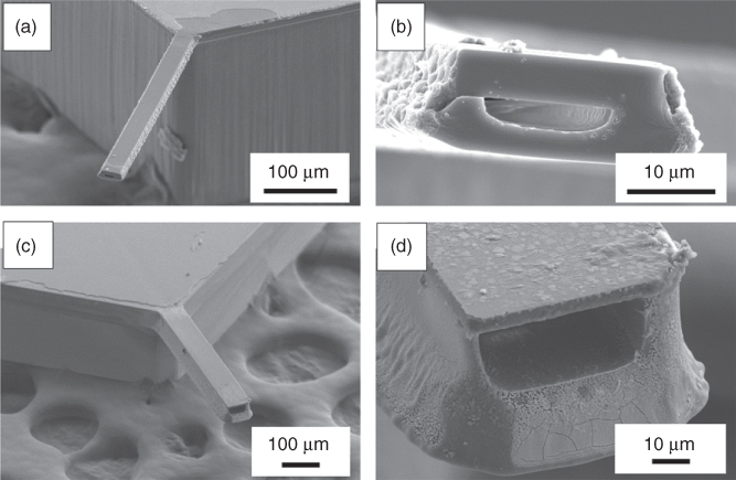
Figure 14.4 SEM micrographs of SU-8 hollow cantilevers with an aperture deliberately defined in the front plane to inspect the cross section. (a) A 12 µm thick cantilever integrating a 3 µm thick and 20 µm wide channel with the corresponding closeup view in (b).
(Martinez et al. (2016) [41]. Copyright 2016. Reproduced with permission of IOP.) (c) A 50 µm thick cantilever integrating a 22 µm thick and 60 µm wide channel with the corresponding closeup view in (d).
(Martinez et al. (2016) [42]. Copyright 2016. Reproduced with permission of RSC.)
Proving the versatility of the microfabrication protocol, hollow SU-8 cantilevers integrating 22 µm thick channels were also fabricated only upon slight adaptation of the original process (Figure 14.4c,d): the positive AZ photoresist was patterned at a higher thickness of 25 µm to confine the copper growth within the channel area. Short spin-coating and limited baking times were compulsory for optimal results. Copper was then electrochemically plated for a longer time until reaching the desired thickness. However, the yield of functional devices was observed to be lower for this modified process probably due to poor wetting during electroplating because of the higher surface hydrophobicity related to the important aspect ratio of the AZ trenches (Figure 14.3d). Such thick hollow cantilevers could benefit from novel applications such as single-cell deposition [42] (see Chapter 15).
14.2 Development of the FluidFM
Having access to such microchanneled cantilevers, we faced the question how to mount them onto a commercial AFM in optical beam detection (OBD) [43] configuration. As depicted in Figure 14.5, we started drilling a channel with a 0.5 mm diameter in the AFM probe holder of our instrument. One aperture is then to be connected with a microfluidic flow control device, while the other with the microchanneled probe chip in correspondence of its reservoir [23].

Figure 14.5 Scheme of the FluidFM in OBD configuration. The microchanneled cantilever is fixed to the drilled probe holder, which is immersed in liquid eventually on top of an inverted optical microscope.
(Meister et al. (2009) [23]. Copyright 2009. Reproduced with permission of ACS.)
From an engineering perspective, the challenge was to achieve a watertight fixation between the reservoir of the microchanneled cantilever and the probe holder of the AFM instrument. Figure 14.6 depicts the different attempted solutions in a chronological order. Initially, we made a ring of a glue at the edge of the aperture of channel in the probe holder (Figure 14.6a). We used a glue having the peculiarity of remaining soft also after drying. We then placed the probe on top of it in correspondence of the reservoir and finally fixed it mechanically with a spring (Figure 14.6b). This configuration was tight at pressure up to 3 bars. In the next iteration, we pressed the probe against a rubber O-ring (Figure 14.6c) using a rigid plastic element to be screwed in the probe holder (Figure 14.6d). Compared with the previous one, this solution offers two advantages: (i) Several probes could be mounted one after the other on the same O-ring, while a new glue ring had to be prepared every time a new tip was mounted. (ii) This configuration was watertight up to 4 bars. Finally, in the current configuration, the probe is glued to the probe holder with a UV-cured cement (Figure 14.6e), and successively the probe holder is clipped to the AFM head (Figure 14.6f).
Figure 14.6 (a) Optical micrograph of a custom “glue” O-ring at the aperture of the drilled probe holder. (b) Photograph of a metallic spring fixing a FluidFM probe to the probe holder having the O-ring like in (a). (c) Optical micrograph of two concentric commercial O-rings at the aperture of the drilled probe holder. (d) Photograph of a machined plastic piece fixing a FluidFM probe with screws to the probe holder having the O-rings like in (c). (e) Photograph of a FluidFM probe glued directly to the current “clip-like” version of the probe holder. (f) Photograph of probe holder in (e) clipped on the AFM head.
The obtained force-controlled nanopipette is characterized by the following properties:
- It can be immersed in liquid.
- The force feedback is active for the gentle approach.
- Topography AFM imaging both in contact and oscillating mode is possible with a spatial resolution determined by the geometry of the apex aperture.
- The microchannel can be filled with any solution (except for those possibly etching the cantilevers or the probe holder).
- In the microchannel both a negative and pressure up to a few bars can be applied.
- It can be mounted on any inverted optical microscope.
The last issue to be verified was how the application of a positive or negative pressure affects the AFM contact between the microchanneled probe and the surface underneath with the force feedback switched on. Indeed, it could have been guessed that the applied pressure induces a mechanical deformation of the cantilevers, eventually causing an unwanted crash of the tip into the substrate. Hence, it was investigated how the system handles variations in pressure when in contact with a substrate. For this purpose, a series of different pressure values ranging from 0 to 1000 mbar and back with steps of Δ = 100 mbar occurring every 5 s was applied to a filled FluidFM probe while the cantilever was kept on a hard surface in contact mode (set point of 1.1 nN) during the entire experiment.
Figure 14.7 illustrates how the system reacts to such changes. Thanks to the fast force feedback control, the resulting net force acting on the substrate remains stable at the fixed set point value although the applied pressure indeed induces a mechanical perturbation on the probe as derived by the movement of the z piezo. From this experiment, it can be concluded that even though the hollow cantilever is influenced by small changes in pressure, the overall system can suppress this effect in order to ensure constant interaction forces with the specimen at all times during an experiment. This property of the FluidFM is truly unique to this technique and can only be indirectly realized by means of alternative methods such as glass micropipettes.
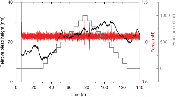
Figure 14.7 Deflection signal (horizontal line, right scale) as function of time of a pyramidal FluidFM probe (apex aperture of 300 nm) in contact (set point 1.1 nN) with a glass slide in bi-distilled water. The channel is filled with bi-distilled water too. Sequential pressure steps are applied in the fluidic circuit (grey line). The z piezo (black line, left scale) compensates the engendered mechanical perturbations keeping the force signal stable.
14.3 Calibration of Hollow Probes: Stiffness and Flow
FluidFM combines force and microfluidics; therefore microchanneled cantilevers must be characterized from both a mechanical and a fluidic point of view in order to draw any quantitative conclusion from the experimental data.
14.3.1 Stiffness
As the cantilever interacts with the specimen surface, the interaction forces deflect the cantilever. The cantilever acts as a spring, and by measuring its deflection, the forces acting upon the cantilever can be determined. For small deflections, the cantilever acts as a linear spring, and the forces can be calculated according to Hooke's law in Eq. (14.1):
In optical beam deflection AFM, bending of the cantilever results in a change of voltage from the photodetector. This signal V can be converted to the deflection in nm with the conversion factor ∝ commonly referred to as inverse optical lever sensitivity (InvOLS). The InvOLS can be calibrated by approaching the cantilever on a hard surface and pushing it downward by a known distance, resulting in a photodetector voltage as shown in Figure 14.8a.
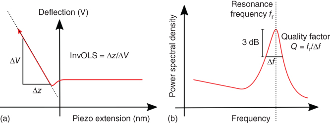
Figure 14.8 Schematic drawing of cantilever calibration measurements. (a) The cantilever is approached on a hard surface. The inverse optical lever sensitivity is determined by the slope in the linear region of the curve. (b) Typical thermal noise spectrum of a cantilever. The resonance frequency and quality factor are used to determine the spring constant using the Sader method.
Commercial cantilevers are specified with a certain spring constant by the manufacturer. However, this is only a gross estimate because the spring constant is subject to high variations due to manufacturing processes, particularly in cantilever thickness, so that each cantilever needs to be calibrated to accurately determine its spring constant.
For a rectangular cantilever with loading at the apex, the spring constant is described in Eq. (14.2) where E, t, w, and l are the cantilever's elastic modulus, thickness, width, and length, respectively:
The length and width can easily be measured using an optical microscope; the thickness and elastic modulus cannot be accurately measured using such a simple technique. However, by using the method developed by Sader et al. [44], the spring constant can be determined by only measuring the cantilever's resonance behavior and its length and width as shown in Eq. (14.3):
The resonance frequency ω and quality factor Q can be obtained by measuring the thermal noise spectrum of the cantilever as shown in Figure 14.8b. Furthermore, ρ is the density and Γi(ω) the imaginary component of the hydrodynamic function of the surrounding liquid obtained from the literature. The Sader method is valid for thin and long cantilevers with uniform cross section along its length [44]. The hollow FluidFM cantilever features stabilizing pillars within the cantilever channel creating a nonuniformity. Nonetheless, numerical simulations investigating the effects of the particular FluidFM cantilever geometries have shown they only have an influence of 1% compared with uniform rectangular cantilevers [45].
The addition of a microchannel into an AFM cantilever increases the cantilever thickness, restricting the final cantilever geometry. This results in spring constants between 0.2 and 2.5 N/m with resonance frequencies of around 80 kHz, making the cantilevers best suited for contact-mode operation. Lateral and torsional forces have not been investigated so far.
14.3.2 Flow
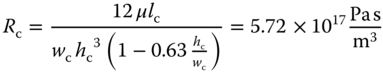
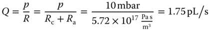
While the calibration for force measurements relies on well-established AFM protocols, novel approaches were required to quantify the flow of liquid through the microchannel of the FluidFM probe. The flow in or out of the cantilever aperture is regulated by applying a pressure at the reservoir of the cantilever clip. Analogous to an electrical circuit where the current is determined by the potential difference across a resistance, the flow Q in the cantilever depends on the applied pressure p and the hydrodynamic resistance R as shown in Eq. (14.4). This makes it possible to estimate the flow through the cantilever while making common assumptions in microfluidics, such as a Newtonian fluid in laminar flow [46]:
The resistance of the channel in the cantilever can be approximated as a rectangular channel with a length lc of 1400 µm, a width wc of 30 µm, and a height hc of 1 µm. In the case of water with viscosity μ, the resistance is calculated in Eq. (14.5):
The 2 µm aperture da through the 350 nm thick cantilever wall la is characterized by the following hydrodynamic resistance (Eq. (14.6)):

The two in-series resistances can be added together to calculate the flow through the cantilever. The resistance of the tubing and that of the reservoir are negligible. At a pressure of 10 mbar, the flow is as follows in Eq. (14.7):
These calculations do not include the effect of the pillars within the cantilever structure or the effect of the pyramid in apex tips. The flow in these structures cannot be calculated analytically; instead, numerical simulations have to be used. The pillar structures inside the cantilever cause an increase in hydrodynamic resistance of about 7%; the inset in Figure 14.9a shows the simulated flow in a cantilever section going around the pillars [45]. The linear relationship between input pressure and flow rate as estimated by the analytical terms with corrections from numerical simulations is shown in Figure 14.9a. The results were validated by tracking fluorescent nanoparticles flowing through the optically transparent cantilever [47].

Figure 14.9 (a) The flow rate increases linearly with the applied pressure as calculated analytically and confirmed experimentally for a 2 µm tipless cantilever. The inset shows the result of the numerical simulations of the flow around the pillars within the cantilever channel. (b) The hydrodynamic resistance of pyramidal cantilevers is dominated by the channel resistance for openings below 500 nm: with decreasing openings, the aperture resistance starts to dominate.
As seen in the analytical calculation, the total hydrodynamic resistance of cantilevers with micrometer-sized apertures is dominated by the channel resistance. This means that the flow rates at a certain pressure are nearly identical for cantilevers with 2 or 8 µm apertures. For pyramidal tips, the influence of the pyramid and aperture size is shown in Figure 14.9b. The aperture only becomes relevant below 500 nm, whereas the hollow volume in the pyramid has a negligible effect.
The combination of analytical and numerical computations makes it possible to estimate the flow at a certain pressure. However, they only describe the continuous flow out of the cantilever. In experiments however, shorter pulses are often used, which are much more complex to simulate, and instead experimental quantification and verification of the simulations are required.
A fluorescent tracer can be added to the cantilever solution to visualize the flow out of the cantilever with fluorescence microscopy. Common tracers are the inexpensive fluorescein or the membrane-impermeable Lucifer yellow. Both are small molecules that diffuse very rapidly. Fluorophores attached to high molecular weight dextran or polyethylene glycol can be used where slower diffusion is advantageous. However, even with high molecular weight tracers, diffusion is still too fast to characterize the volumes released from the cantilever. The following method avoids the diffusion issue by first injecting the fluorescent solution into oil. Consequently, the method is unsuited for oil-soluble substances.
As a reference, the fluorescence intensity per volume can be determined by injecting the fluorescent solution into immersion oil, resulting in spherical droplets that are contained in the immiscible oil [48]. The droplet volume is simply calculated by measuring the droplet diameter, while the total fluorescence intensity is calculated by integrating the fluorescence intensity of a fluorescence image of the droplet. It is crucial that the imaging conditions are consistent and the background fluorescence is accounted for by subtracting the background fluorescence intensity. Plotting the fluorescence intensity against the droplet volumes gives a calibration curve to determine the released volumes from the more easily measurable fluorescence intensity.
Using this technique, the volumes injected into cells were determined for intranuclear injection into HeLa cells [48]. The total fluorescence intensity of the cell was measured before and after injection using the same imaging condition as for the calibration curve. The measured increase in fluorescence was then converted to volume using the calibration plot. The injected volumes for different pressure pulses are shown in Figure 14.10b.
Measuring the total fluorescence intensity is more challenging in an open environment compared with the confined space of a cell due to rapid diffusion. Yet, the diffusion effect can be limited by using microwells [49]. The total fluorescence intensity before and after release of a fluorescent tracer into microwells of 500 µm × 500 µm × 60 µm was measured to determine the flow rate with an 8 µm tipless cantilever. Analogous to the injection into cells, the injected volumes are shown in Figure 14.10b. Using those measurements, the flow rate results in 64 ± 2 fL/s mbar for the 8 µm tipless cantilever.
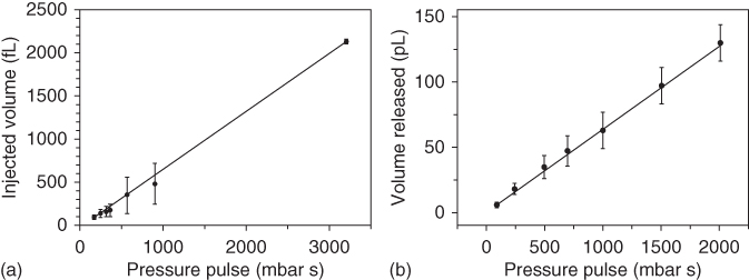
Figure 14.10 Calibration of released volume for 300 nm and 8 µm aperture cantilevers. (a) The volume of solution injected into HeLa cells using a pyramidal cantilever with a triangular 300 nm side aperture.
(Guillaume-Gentil et al. (2013) [48]. Copyright 2013. Reproduced with permission of Wiley.) (b) The volume of solution released into a microwell with an 8 µm aperture tipless cantilever.
(Guillaume-Gentil et al. (2014) [49]. Copyright 2014. Reproduced with permission of RSC.)
The previous methods are only valid if the flow through the cantilever does not change over the course of the experiments. However, interaction with the substrate especially cell membranes can lead to a reduced flow due to partial clogging of the aperture. The following procedure makes it possible to regularly monitor the flow out of the cantilever during an experiment. The cantilever is retracted several 100 µm up and away from the surface, and a constant pressure is applied. The resulting flow out of the cantilever and the diffusion into the solution creates a cloud with a characteristic diameter. The characteristic diameter can be measured by plotting the fluorescence intensity profile and measuring the full width at half maximum (FWHM). Any change in flow rate can be detected by monitoring the cloud diameter. Due to the low flow rates, the previously released volume and its effects are negligible compared with the total volume of the solution. Nevertheless, for certain biomolecules it is advisable to switch to a different dish while performing the monitoring procedure.
14.4 FluidFM as Lithography Tool in Liquid
Fabrication of functional materials in reduced feature size has been considered essential for various applications such as integrated circuits, memory devices, display units, and biosensor applications. Several approaches such as photolithography, electron beam lithography, and FIB lithography are based on standard lithographical methods and have been widely explored especially in semiconductor industrial processes [50–53]. However, these conventional fabrication technologies were often limited by the needs of multistep processes and high operating costs. AFM-based lithography represents an alternative as a tool for local surface modification via direct molecular deposition or mechanical indentation. The technique can be used to pattern a wide range of materials including metallic structures, polymers, and biological molecules at a desired position and with a desired geometrical shape. The various AFM-based deposition techniques have been categorized into whether the deposition occurs in air (eventually at a controlled humidity), such as dip pen nanolithography (DPN), nanodispenser (NADIS), and nanofountain pens, or in liquid, by using electrochemical (EC) AFM (AFM SECM): see the comprehensive reviews on AFM-based lithography [54–56].
14.4.1 Patterning Nanoparticles
The FluidFM can be operated as lithography tool in liquid to locally deposit molecules or nanosized objects dissolved in the solution contained in the microchannel. To investigate the fundamentals of this patterning process [57], we chose a system trying to minimize any ambiguity: we used 25 nm fluorescent polystyrene nanoparticles (psNP) to have an immediate visual control, while to promote the adhesion of the negatively charged psNP onto the substrate, thus blocking surface Brownian diffusion, we coated the glass with a polyethylenimine (PEI), a polycation. Overpressure was applied to dispense of the psNP after the cantilever was approached and kept in contact by force feedback. To determine the effect on deposition of the different external parameters such as pressure, tip velocity (respectively, contact time), and force set point, we decided to draw lines at constant velocity. Indeed, the transient flow out of the tip is unstable during the approach and retraction of the tip, since the distance between aperture of tip and surface is changed (and thus the flow resistance), significantly affecting the deposition.
From the fluorescence image of Figure 14.11a, the smaller the velocity (i.e., the longer the contact time), the brighter the fluorescence, meaning the higher was the number of deposited psNP. As intuitively expected, we also noted that the higher the pressure applied, the higher was the number of deposited psNP. For a quantitative assessment of the psNP distribution and coverage, the obtained patterns were inspected ex situ using scanning electron microscopy (Figure 14.11b,c), which confirmed furthermore that nanoparticle deposition mostly happens under the cantilever tip in a single layer. In each line, a psNP gradient can be noticed from the middle of the line: the minimum achievable FWHM corresponds to the double of aperture size. The process of psNP deposition could be rationalized as a random sequential adsorption [58]. The jamming limit is defined as the maximum psNP coverage Θmax, where psNP may no more remain absorbed on the surface. This depends on the effective psNP size with the contribution of the physical radius and the ionic strength of the solution. As shown in Figure 14.12a, each curve according to different contact time with constant pressure could be fitted to Eq. (14.8), derived from the simple kinetic equation for the Langmuir model:
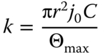
Θmax was experimentally measured by immersing the PEI-coated glass slide for 30 min in a psNP solution like that in the microchannel until saturation and then examining it at the SEM. Its value was 16% and is shown in the graphs of Figure 14.12 as a dashed line. In the data analysis, we assumed that the salt concentration under the tip is equal to buffer solution.
k is the rate constant of the process, which is determined by the radius of the nanoparticles r, the mass transfer rate j0, and the bulk concentration of the psNP solution C. From the rate constant, the volumetric flow rate and the hydrodynamic resistance were determined by Eq. (14.10), where A is the unit area of the line and ![]() the applied pressure:
the applied pressure:


Figure 14.11 (a) Fluorescent image of the nanoparticle lines upon deposition with 0.5 mbar and different tip velocities from 10 to 160 µm/s onto a glass slide in a buffer solution (HEPES 10 mM, pH 7.4). AFM and SEM images of nanoparticle lines deposited with (b) a pressure of 0.5 mbar and different tip velocities and (c) a tip velocity of 80 µm/s and pressures between 0.5 and 2.0 mbar.
(Grüter et al. (2013) [57]. Copyright 2013. Reproduced with permission of RSC.)
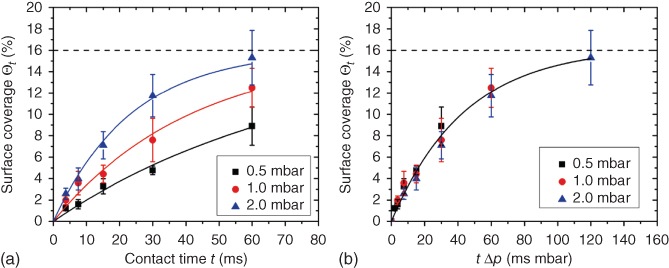
Figure 14.12 (a) Surface coverage as a function of the contact time t for pressures between 0.5 and 2.0 mbar. Solid line: fitted curves using the Langmuir model (R2 ≥ 0.98, k is the only fitting parameter). The dashed line corresponds to the experimental value of Θmax = 16%. (b) Normalized surface coverage as a function of the product of pressure and contact time t. Solid line: Fitted curves using the Langmuir model (k is the only fitting parameter).
(Grüter et al. (2013) [57]. Copyright 2013. Reproduced with permission of RSC.)
The volumetric flow rate can be estimated around 4 aL/ms, while the hydrodynamic resistance Rtot was in the range of 2.5 × 10¹⁹ Pa s/m3. It can be rationalized as the sum of Rcant and Rcontact, where Rcant is the hydrodynamic resistance of the cantilever and Rcontact is the resistance, which is dependent on the geometry of the space between tip and substrate. Since the cross section of microchannel and tip aperture is rectangular, the hydrodynamic resistance of the cantilever Rcant can be analytically modeled, giving a value of ∼1018 Pa s/m3, which means the Rcontact is in the range of 2.4 × 10¹⁹ Pa s/m3 and affects more strongly the flow rate. In the normalized graph (Figure 14.12b), a single absorption curve was attained by merging of the data for the different pressures, indicating that the number of deposited nanoparticles is dependent only on the dispensed volume, which can be adjusted by applied pressure and contact time. The force set point was also observed to influence the patterning process because, by changing the aperture-surface separation, it affects Rcontact and thus the flow.
Apart from changing the pressure, tip velocity, and force set point, we examined the effect of another external parameter: the ionic strength of the liquid environment. In this work, negatively charged gold nanoparticles (AuNP) were delivered onto a glass surface coated with PEI to form electrical interconnections [59]. In contrast to the previous experiment, tipless cantilevers with a 2 µm aperture were used since AuNP quickly accumulate in the microchannel because the highly concentrated salt outside rapidly diffuses into the microchannel, inducing accumulation and thus increasing the change for clogging. The AuNP deposition was followed in situ under the dark-field microscope, instead of the fluorescent microscope (Figure 14.13a,b). As expected, the higher the ionic concentration of the liquid environment was, the higher the deposited AuNP amount could be observed. Through the AFM imaging, we found that the deposited layer was indeed an AuNP multilayer, meaning that stacking of gold nanoparticles has occurred due to the smaller Debye length at high salt concentration.
Figure 14.13 Dark-field image of a deposited AuNP line with the contact time of 7.4 min (tip velocity of 0.9 µm/s and repeated writing of 50 times) (a) before and (b) after gold annealing. (c) SEM image of the gold layer after annealing. (d) Measured resistance during gold annealing of deposited AuNP at 150 mM of high salt concentration. (e) SEM image of the gold layer after annealing.
(Grüter et al. (2015) [59]. Copyright 2015. Reproduced with permission of IOP.)
To get a conductive AuNP layer, the deposited AuNP must be “in contact” to enable electron transport from particle to particle. To finalize the protocol, not only the contact time and the ionic strength were varied, but also the particle size. In the final recipe, in order to overcome the coagulation issue (Figure 14.13c), 5 nm AuNP were mixed with 20 nm ones. After annealing of the deposited stripes up to 250 °C in air, we measured a resistivity of 1.2 × 10⁻⁶ Ω m (Figure 14.13d), improving by more than two orders of magnitude compared with the value directly after deposition. We hypothesized that bigger-size nanoparticles have not been completely melted during the annealing step, while the smaller particles did and thus established an electrically conductive path through the layer (Figure 14.13e).
14.4.2 Electrochemical 2D Patterning and 3D Printing
Among the various ways for local surface modification with scanning probe techniques, EC methods are particularly attractive since the patterning reaction may be switched on and off on demand, and there exists a wide range of molecules that may be attached to a surface via EC reactions. It is therefore a straightforward step to combine FluidFM with an EC setup as well: combining the advantages of microfluidics with the inherent force feedback and imaging capability of an AFM, FluidFM is an attractive tool in the domain of local EC surface modification. EC-patterning techniques have been developed for most scanning probe techniques [60]. For example, Kolb used the tip of a scanning tunneling microscope (STM) as an EC-nanopatterning tool for copper or gold [61]. The scanning electrochemical microscope (SECM) [62] developed in the 1990s by Bard is based on an insulated ultramicroelectrode (UME) that is brought close to a substrate. This enables EC patterning in various configurations [63]. The probe may be used to generate reactive species locally in the so-called tip generation mode [64], or an EC-patterning reaction is localized by confining the electric field to the region between the UME and the substrate. A particular advantage of SECM is the inherent capability to measure local reactivity of a substrate after the modification. For example, Liu et al. have used SECM for both the local EC reduction of graphene oxide to graphene and the subsequent imaging control using the substrate generation–tip collection mode of SECM [65].
In addition to microelectrodes, glass micro- and nanopipettes have been used for patterning applications as well. Here, a micro-EC cell in the liquid meniscus between the pipette orifice and the substrate is created. This enables so-called meniscus-confined patterning reactions and allows for high-resolution patterning of various moieties [60]. The challenge with these techniques is the precise approach of the pipette to the substrate and maintaining a stable meniscus and a fixed pipette-substrate distance. Many approaches to solve this challenge exist [66]; for example, Iwata et al. reported a system that relies on detecting the shear forces between the pipette tip and the substrate: the mechanical resonance frequency of the pipette may be measured using a piezo for the excitation and a laser and a photodiode for the amplitude measurement. In this way, changes of the resonance due to shear forces between the tip and the substrate may be observed and used for feedback [67]. EC patterning was demonstrated with such glass pipettes in liquid environment as well [20]. Scanning electrochemical cell microscopy (SECCM) developed by the Unwin group uses double-barreled pipettes where each barrel contains an electrode. The ionic current between these two electrodes is a function of the gap between the substrate and the pipette aperture. Thus, this current may be used as a control signal to maintain a desired pipette height above the substrate similar to the scanning ion conductance microscope (SICM) [12, 68, 69]. SECCM enables EC surface modification with sub-micrometer resolution, for example, with conductive polymers [70] or by electrografting [71]. A common disadvantage of most EC deposition methods is the requirement of a polarized substrate, that is, a substrate that is both conductive and may be electrically contacted. Recently, a new technique termed scanning bipolar cell (SBC) has overcome the latter need by exploiting the parallel resistance between the substrate (electric resistance) and the electrolyte (ionic resistance) [72, 73].
The first 2D EC-patterning applications with FluidFM were demonstrated in a simple approach where the FluidFM probe is used as a local supply of reactants in a macro EC cell (Figure 14.14) [74].
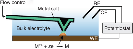
Figure 14.14 Schematic of FluidFM for local electrochemical patterning applications. In a standard electrochemical cell, the cantilever is used to deliver precursor ions to the polarized substrate locally. The ions are reduced locally, thus enabling the electrochemical “writing” of patterns. Various materials may be patterned; the example shown here is the electroplating of a metal (M) via cathodic reduction of supplied metal ions (Mz+). Experiments with an RE inserted in the channel were not successful because of the lack of control of the applied potential probably due to the too high ohmic resistance drop along the channel.
(Hirt et al. (2015) [74]. Copyright 2015. Reproduced with permission of RSC.)
As demonstration systems, the well-known electroplating of copper and the versatile electrografting of benzene layers via reduction of diazonium salts were chosen [75–77]. The used EC cell consisted of a droplet of electrolyte suspended between the flat AFM probe holder and the substrate. This droplet was usually held in place by a hydrophobic PDMS ring placed on the substrate. While the conductive substrate represented the working electrode (WE) in this cell, an additional silver and platinum wire served as quasi-reference electrode (QRE) and counter electrode (CE), respectively. In the used configuration, these two wires were mounted on the FluidFM fluidic connector with UV-curable epoxy to be as closest as possible to the tip aperture. The EC deposition process consisted of approaching the cantilever to the substrate, applying a desired overpressure to induce a flow of reactants from the tip aperture, and switching on the deposition potential.
FluidFM could be successfully used for EC patterning with this setup: gold and indium tin oxide (ITO) thin films were modified by electroplating with copper and also by covalently linking thin layers of organic moieties containing nitro groups (Figure 14.15).

Figure 14.15 Local covalent modification of conductive surfaces. (a) Illustration of the underlying principle: aryl rings containing a nitro and a diazo group are reduced, splitting off nitrogen and leaving an aryl radical, which in turn may covalently bind to the substrate. (b) A FluidFM probe (300 nm aperture) containing the diazonium salt was approached to an ITO substrate for various time spans at a deposition potential of −0.7 V versus the silver QRE, and just afterwards used for standard AFM topography imaging in contact mode. c) As in b), AFM image obtained with the FluidFM probe of a line pattern in the shape of an aryl ring containing a diazo group. The probe was moved at a speed of 4 µm s−1 during the deposition. d) Corresponding SEM image of the same pattern after drying and rinsing.
(Hirt et al. (2015) [74]. Copyright 2015. Reproduced with permission of RSC.)
In the deposition of such thin layers, a major advantage of the FluidFM technology is revealed after the deposition process itself: the same probe may be used for deposition and in situ characterization of the electrografted structures via standard AFM imaging. In the case of electrografting of nitrobenzene layers, such imaging revealed a layer thickness of ∼5 to 6 nm. Furthermore, the shape and characteristics of deposited features may be studied, for example, with respect to their dependence on the applied overpressure or the deposition time (Figure 14.15b–d ).
Microchanneled cantilevers with an electrode inside the fluidic circuit were used by Geerlings et al. for electrospray experiments [78], thus establishing a switchable nanoscale deposition technique for polar and ionic components. By tuning the apex-surface separation as well as the pulse intensity and duration, minutest dried deposits of ∼80 nm were obtained, which is significantly smaller than results obtained with electrospray deposition from pulled capillaries.
In the case of local EC deposition, interesting options arise if the deposited material is itself conductive. In this case, the deposition effectively changes the shape of the substrate electrode without removing its conductivity. Thus, the deposition process is in principle not limited by substrate passivation. In this case, the FluidFM can be used as an EC 3D printer on the micrometer scale.
3D microfabrication based on local electrodeposition was proposed in the early days of scanning probes, and various techniques have been investigated since, which are again divided in those relying on microelectrodes and those employing micropipettes to achieve the localized electrodeposition. In the first group, a microelectrode is used as CE for an electroplating process and brought close to a conductive surface, which is the WE in an EC cell. This process, introduced by Madden and Hunter [79, 80] and later termed metal anode-guided electroplating (MAGE) [81] or localized electrochemical deposition (LECD) [82] by other groups, is capable of producing wirelike structures in a single-step process. The underlying phenomena and their influence on the resulting wire-shaped structures have been studied during the recent years [82–86], whereas non-wirelike geometries have not been demonstrated to date. Micropipettes have been used for the EC fabrication of 2.5D and 3D structures as well. For example, Suryavanshi and Yu employed nanopipettes for the fabrication of straight platinum nanowires [87]. In an advanced application, custom-shaped nanopipettes were used by Hu and Yu for meniscus-confined fabrication of electric interconnect wires with both excellent resolution (tens of nanometers) and resistivity (∼3 × 10⁻⁸ Ω m) [88]. Their setup relied on very precise current measurements (less than picoampere resolution) and customized pipette apertures obtained with FIB milling such that it was possible to establish a meniscus sideways, thus allowing horizontal printing of metal wires. Recently, Seol et al. used pulsed currents to achieve electroplating only at the meniscus edge, obtaining tubelike structures. 3D deposition of polypyrrole pillars was achieved with regular glass micropipettes by Aydemir et al. [89], and polyaniline pillars were fabricated using SECCM by the Unwin group, demonstrating the potential to use theta-pipettes for 3D EC fabrication as well [70].
The FluidFM EC deposition setup offers two promising benefits for EC 3D microfabrication: First, the inherent force feedback allows for the detection of touching events between the deposited structure and the cantilever aperture. Second, the liquid environment avoids the need of a liquid meniscus as opposed to techniques operating in air. This meniscus has to be established on a micrometer scale each time the probe approaches a new position, which may be difficult especially for more complex structures. Both these FluidFM features prove to be key advantages for an automated 3D printing system: the force feedback gives information about the printing progress, while the independence from a liquid meniscus allows for a reliable procedure without the need of constant monitoring.
In the first in-lab realization, the same deposition setup as for 2D surface patterning (Figure 14.14) was used. In addition, a control routine based on LabVIEW® was written to automate the printing process [90]. Using data acquisition cards, the program controls the x-, y-, and z-position of the FluidFM probe as well as the applied overpressure. In addition, the deflection signal is monitored.
For 3D microfabrication, the FluidFM probe is approached to a small distance (usually <1 µm) from the current printing position, and the deposition process is started by applying an overpressure and switching on the deposition potential. Due to the confinement of metal ions to the region under the probe aperture, a metal deposit thus forms only in this region. Eventually, the deposit touches the FluidFM probe, leading to a change in the cantilever deflection, which is monitored by the control software. At this point, the probe may be moved to the next printing position and the process is repeated. Since no liquid meniscus is required, approaching the next position is achieved immediately and reliably.
In this fashion, various copper structures were fabricated using a copper sulfate solution, where the shape was defined by the probe movement during the deposition process. The method allows for fabrication of wirelike structures similar to those previously reported by Hu and Yu using glass pipettes in air [88]. Additionally, more complex 2.5D and 3D objects such as the wall and the vase in Figure 14.16 are enabled via the ease of automation. With these preliminary results, FluidFM might become a new, template-free, robust, and automated tool for 3D microfabrication of metals. Furthermore, this method should be readily adaptable to print metals beyond copper. For example, printing gold or silver could enable direct writing of prototype structures with tunable plasmonic properties, while magnetic alloys based on cobalt or nickel could be used for microrobots that are actuated in a rotated magnetic field [91]. Finally, electrodeposition is suitable for a broad variety of materials beyond metals, for example, conductive polymers such as polyaniline [70]. Therefore, adjusting the setup parameters such as concentrations, surrounding electrolyte, and deposition potentials for new materials will be the focus of future studies.
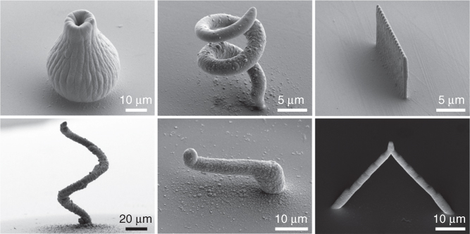
Figure 14.16 Various metal structures fabricated by electrochemical 3D deposition with FluidFM. The shapes range from 2.5D such as a wall to true 3D shapes such as a vase or helix.
(Hirt et al. (2016) [90]. Copyright 2016. Reproduced with permission of Wiley.)
14.5 Conclusions and Outlook
The combination of microfluidics and AFM delivers a versatile tool: on the one hand, every soluble molecule or nano-object can be stored in the channel, and on the other hand by means of the force control, whatever hard or soft surface can be approached followed by precisely located dispensing. Furthermore, thanks to the watertight connection between probe chip and AFM probe holder, the FluidFM can be operated in liquid, the environment of biology and electrochemistry.
Although 10 years have passed from the very first idea and the tool is reliably working, plenty of ideas can be envisioned for its further development: in the direction of automation (e.g., serial approach of different locations previously selected on the screen of the optical microscope), of multichannel probes (e.g., sequential delivery of different molecules each stored in a different channel embedded in the same cantilever), of microfabrication (e.g., hollow conical tips), and of detection (e.g., piezoresistive electrodes toward a multi-pipette system).
Acknowledgments
The development of the FluidFM was supported by the Swiss Innovation Promotion Agency CTI-KTI, by the Swiss National Science Foundation (SNSF), by the Promedica Foundation (Chur, CH), and by the Swiss programs SystemsX and Nano-Tera.
We would like to thank Michael Gabi and Pablo Dörig (Cytosurge AG, Switzerland), Edin Sarajlic (SmartTip BV, The Netherlands), and Patrick Frederix (Nanosurf AG, Switzerland) for their constant support. André Meister, Jérôme Polesel-Maris, Philippe Niedermann, Joanna Bitterli, Martha Liley, and Harry Heinzelmann (CSEM SA, Switzerland) are acknowledged for the initial collaboration. We are indebted to Stephen Wheeler and Martin Lanz (LBB Workshop) for their technical skills as well as to all other past and present students plus postdoctoral fellows involved in the FluidFM projects for their passionate contribution.
References
- 1 Barber, M.A.A. (1904) A new method of isolating micro-organisms. J. Kansas Med. Soc., 4, 489–494.
- 2 Terreros, D.A. and Grantham, J.J. (1982) Marshall Barber and the origins of micropipette methods. Am. J. Physiol., 242, F293–F296.
- 3 Hochmuth, R.M. (2000) Micropipette aspiration of living cells. J. Biomech., 33 (1), 15–22.
- 4 Ishøy, T., Kvist, T., Westermann, P., and Ahring, B.K. (2006) An improved method for single cell isolation of prokaryotes from meso-, thermo- and hyperthermophilic environments using micromanipulation. Appl. Microbiol. Biotechnol., 69 (5), 510–514.
- 5 Capecchi, M.R. (1980) High efficiency transformation by direct microinjection of DNA into cultured mammalian cells. Cell, 22 (2), 479–488.
- 6 Zhang, Y. and Yu, L.-C. (2008) Single-cell microinjection technology in cell biology. BioEssays, 30 (6), 606–610.
- 7 Neumann, E., Kakorin, S., and Tœnsing, K. (1999) Fundamentals of electroporative delivery of drugs and genes. Bioelectrochem. Bioenerg., 48 (1), 3–16.
- 8 Haas, K., Sin, W.-C., Javaherian, A., Li, Z., and Cline, H.T. (2001) Single-cell electroporation for gene transfer in vivo. Neuron, 29 (3), 583–591.
- 9 Neher, E. and Sakmann, B. (1976) Single-channel currents recorded from membrane of denervated frog muscle fibres. Nature, 260 (5554), 799–802.
- 10 Hamill, O.P., Marty, A., Neher, E., Sakmann, B., and Sigworth, F.J. (1981) Improved patch-clamp techniques for high-resolution current recording from cells and cell-free membrane patches. Pflügers Arch. Eur. J. Physiol., 391 (2), 85–100.
- 11 Margrie, T.W., Meyer, A.H., Caputi, A., Monyer, H., Hasan, M.T., Schaefer, A.T., Denk, W., and Brecht, M. (2003) Targeted whole-cell recordings in the mammalian brain in vivo. Neuron, 39 (6), 911–918.
- 12 Hansma, P., Drake, B., Marti, O., Gould, S., and Prater, C. (1989) The scanning ion-conductance microscope. Science, 243 (4891), 641–643.
- 13 Korchev, Y.E., Bashford, C.L., Milovanovic, M., Vodyanoy, I., and Lab, M.J. (1997) Scanning ion conductance microscopy of living cells. Biophys. J., 73 (2), 653–658.
- 14 Novak, P., Li, C., Shevchuk, A.I., Stepanyan, R., Caldwell, M., Hughes, S., Smart, T.G., Gorelik, J., Ostanin, V.P., Lab, M.J., Moss, G.W.J., Frolenkov, G.I., Klenerman, D., and Korchev, Y.E. (2009) Nanoscale live-cell imaging using hopping probe ion conductance microscopy. Nat. Methods, 6 (4), 279–281.
- 15 Stephens, D.J. and Pepperkok, R. (2001) The many ways to cross the plasma membrane. Proc. Natl. Acad. Sci. U.S.A., 98 (8), 4295–4298.
- 16 Proksch, R., Lal, R., Hansma, P.K., Morse, D., and Stucky, G. (1996) Imaging the internal and external pore structure of membranes in fluid: TappingMode scanning ion conductance microscopy. Biophys. J., 71 (4), 2155–2157.
- 17 Lewis, A., Kheifetz, Y., Shambrodt, E., Radko, A., Khatchatryan, E., and Sukenik, C. (1999) Fountain pen nanochemistry: atomic force control of chrome etching. Appl. Phys. Lett., 75 (17), 2689.
- 18 Drake, B., Randall, C., Bridges, D., and Hansma, P.K. (2014) A new ion sensing deep atomic force microscope. Rev. Sci. Instrum., 85 (8), 083706.
- 19 Lu, Z., Chen, P.C.Y., Nam, J., Ge, R., and Lin, W. (2007) A micromanipulation system with dynamic force-feedback for automatic batch microinjection. J. Micromech. Microeng., 17 (2), 314–321.
- 20 Ito, S. and Iwata, F. (2011) Nanometer-scale deposition of metal plating using a nanopipette probe in liquid condition. Jpn. J. Appl. Phys., 50 (8), 08LB15.
- 21 An, S., Lee, K., Kim, B., Noh, H., Kim, J., Kwon, S., Lee, M., Hong, M.-H., and Jhe, W. (2014) Nanopipette combined with quartz tuning fork-atomic force microscope for force spectroscopy/microscopy and liquid delivery-based nanofabrication. Rev. Sci. Instrum., 85 (3), 033702.
- 22 Binnig, G., Quate, C.F., and Gerber, C. (1986) Atomic force microscope. Phys. Rev. Lett., 56 (9), 930–933.
- 23 Meister, A., Gabi, M., Behr, P., Studer, P., Vörös, J., Niedermann, P., Bitterli, J., Polesel-Maris, J., Liley, M., Heinzelmann, H., and Zambelli, T. (2009) FluidFM: combining atomic force microscopy and nanofluidics in a universal liquid delivery system for single cell applications and beyond. Nano Lett., 9 (6), 2501–2507.
- 24 Guillaume-Gentil, O., Potthoff, E., Ossola, D., Franz, C.M., Zambelli, T., and Vorholt, J.a. (2014) Force-controlled manipulation of single cells: from AFM to FluidFM. Trends Biotechnol., 32 (7), 381–388.
- 25 Meister, A., Jeney, S., Liley, M., Akiyama, T., Staufer, U., de Rooij, N.F., and Heinzelmann, H. (2003) Nanoscale dispensing of liquids through cantilevered probes. Microelectron. Eng., 67–68, 644–650.
- 26 Meister, A., Liley, M., Brugger, J., Pugin, R., and Heinzelmann, H. (2004) Nanodispenser for attoliter volume deposition using atomic force microscopy probes modified by focused-ion-beam milling. Appl. Phys. Lett., 85 (25), 6260.
- 27 Deladi, S., Tas, N.R., Berenschot, J.W., Krijnen, G.J.M., de Boer, M.J., de Boer, J.H., Peter, M., and Elwenspoek, M.C. (2004) Micromachined fountain pen for atomic force microscope-based nanopatterning. Appl. Phys. Lett., 85 (22), 5361.
- 28 Moldovan, N., Kim, K.-H., and Espinosa, H.D. (2006) Design and fabrication of a novel microfluidic nanoprobe. J. Microelectromech. Syst., 15 (1), 204–213.
- 29 Hug, T.S., Biss, T., de Rooij, N.F., and Staufer, U. (2005) Generic fabriction technology for transparent and suspended microfluidic and nanofluidic channels. The 13th International Conference on Solid-State Sensors, Actuators and Microsystems, 2005. Digest of Technical Papers. TRANSDUCERS '05., Vol. 2, pp. 1191–1194.
- 30 Meister, A., Polesel-Maris, J., Niedermann, P., Przybylska, J., Studer, P., Gabi, M., Behr, P., Zambelli, T., Liley, M., Vörös, J., and Heinzelmann, H. (2009) Nanoscale dispensing in liquid environment of streptavidin on a biotin-functionalized surface using hollow atomic force microscopy probes. Microelectron. Eng., 86 (4–6), 1481–1484.
- 31 Kato, N., Kawashima, T., Shibata, T., Mineta, T., and Makino, E. (2010) Micromachining of a newly designed AFM probe integrated with hollow microneedle for cellular function analysis. Microelectron. Eng., 87 (5–8), 1185–1189.
- 32 Dörig, P., Stiefel, P., Behr, P., Sarajlic, E., Bijl, D., Gabi, M., Vörös, J., Vorholt, J.A., and Zambelli, T. (2010) Force-controlled spatial manipulation of viable mammalian cells and micro-organisms by means of FluidFM technology. Appl. Phys. Lett., 97 (2), 023701.
- 33 Berenschot, E.J.W., Burouni, N., Schurink, B., van Honschoten, J.W., Sanders, R.G.P., Truckenmuller, R., Jansen, H.V., Elwenspoek, M.C., van Apeldoorn, A.A., and Tas, N.R. (2012) 3D nanofabrication of fluidic components by corner lithography. Small, 8 (24), 3823–3831.
- 34 Genolet, G., Brugger, J., Despont, M., Drechsler, U., Vettiger, P., de Rooij, N.F., and Anselmetti, D. (1999) Soft, entirely photoplastic probes for scanning force microscopy. Rev. Sci. Instrum., 70 (5), 2398.
- 35 Thaysen, J., Yal inkaya, A.D., Vettiger, P., and Menon, A. (2002) Polymer-based stress sensor with integrated readout. J. Phys. D Appl. Phys., 35 (21), 2698–2703.
- 36 Calleja, M., Nordström, M., Álvarez, M., Tamayo, J., Lechuga, L.M., and Boisen, A. (2005) Highly sensitive polymer-based cantilever-sensors for DNA detection. Ultramicroscopy, 105 (1–4), 215–222.
- 37 Gaitas, H.R. (2014) SU-8 microcantilever with an aperture, fluidic channel, and sensing mechanisms for biological and other applications. J. Micro/Nanolithogr. MEMS MOEMS, 13 (3), 1–8.
- 38 Blanco, F.J., Agirregabiria, M., Garcia, J., Berganzo, J., Tijero, M., Arroyo, M.T., Ruano, J.M., Aramburu, I., and Mayora, K. (2004) Novel three-dimensional embedded SU-8 microchannels fabricated using a low temperature full wafer adhesive bonding. J. Micromech. Microeng., 14 (7), 1047–1056.
- 39 Bilenberg, B., Nielsen, T., Clausen, B., and Kristensen, A. (2004) PMMA to SU-8 bonding for polymer based lab-on-a-chip systems with integrated optics. J. Micromech. Microeng., 14 (6), 814–818.
- 40 Zhang, Z., Zhao, P., Xiao, G., Watts, B.R., and Xu, C. (2011) Sealing SU-8 microfluidic channels using PDMS. Biomicrofluidics, 5 (4), 046503.
- 41 Martinez, V., Behr, P., Drechsler, U., Polesel-Maris, J., Potthoff, E., Vörös, J., and Zambelli, T. (2016) SU-8 hollow cantilevers for AFM cell adhesion studies. J. Micromech. Microeng., 26 (5), 055006.
- 42 Martinez, V., Forró, C., Weydert, S., Aebersold, M.J., Dermutz, H., Guillaume-Gentil, O., Zambelli, T., Vörös, J., and Demkó, L. (2016) Controlled single-cell deposition and patterning by highly flexible hollow cantilevers. Lab Chip, 16 (9), 1663–1674.
- 43 Meyer, G. and Amer, N.M. (1988) Novel optical approach to atomic force microscopy. Appl. Phys. Lett., 53 (12), 1045.
- 44 Sader, J.E., Sanelli, J.A., Adamson, B.D., Monty, J.P., Wei, X., Crawford, S.A., Friend, J.R., Marusic, I., Mulvaney, P., and Bieske, E.J. (2012) Spring constant calibration of atomic force microscope cantilevers of arbitrary shape. Rev. Sci. Instrum., 83 (10), 103705.
- 45 Dörig, S.P. (2013) Manipulating Cells and Colloids with FluidFM, Doctoral dissertation, ETH Zurich.
- 46 Hardt, S. and Schönfeld, F. (eds) (2007) Microfluidic Technologies for Miniaturized Analysis Systems, Springer US, Boston, MA.
- 47 Dörig, P., Ossola, D., Truong, A.M., Graf, M., Stauffer, F., Vörös, J., and Zambelli, T. (2013) Exchangeable colloidal AFM probes for the quantification of irreversible and long-term interactions. Biophys. J., 105 (2), 463–472.
- 48 Guillaume-Gentil, O., Potthoff, E., Ossola, D., Dörig, P., Zambelli, T., and Vorholt, J.A. (2013) Force-controlled fluidic injection into single cell nuclei. Small, 9 (11), 1904–1907.
- 49 Guillaume-Gentil, O., Zambelli, T., and Vorholt, J.A. (2014) Isolation of single mammalian cells from adherent cultures by fluidic force microscopy. Lab Chip, 14 (2), 402–414.
- 50 Klauk, H., Gundlach, D.J., Bonse, M., Kuo, C.C., and Jackson, T.N. (2000) A reduced complexity process for organic thin film transistors. Appl. Phys. Lett., 76 (13), 1692–1694.
- 51 Fujita, J., Ohnishi, Y., Ochiai, Y., and Matsui, S. (1996) Ultrahigh resolution of calixarene negative resist in electron beam lithography. Appl. Phys. Lett., 68 (9), 1297.
- 52 Bach, L., Reithmaier, I.P., Forchel, A., Gentner, J.L., and Goldstein, L. (2001) Multiwavelength laterally complex coupled distributed feedback laser arrays with monolithically integrated combiner fabricated by focused-ion-beam lithography. Appl. Phys. Lett., 79 (15), 2324.
- 53 Goodberlet, J.G. (2000) Patterning 100 nm features using deep-ultraviolet contact photolithography. Appl. Phys. Lett., 76 (6), 667–669.
- 54 Xie, X.N., Chung, H.J., Sow, C.H., and Wee, A.T.S. (2006) Nanoscale materials patterning and engineering by atomic force microscopy nanolithography. Mater. Sci. Eng. R, 54 (1–2), 1–48.
- 55 Salaita, K., Wang, Y., and Mirkin, C.A. (2007) Applications of dip-pen nanolithography. Nat. Nanotechnol., 2 (3), 145–155.
- 56 Garcia, R., Knoll, A.W., and Riedo, E. (2014) Advanced scanning probe lithography. Nat. Nanotechnol., 9 (8), 577–587.
- 57 Grüter, R.R., Vörös, J., and Zambelli, T. (2013) FluidFM as a lithography tool in liquid: spatially controlled deposition of fluorescent nanoparticles. Nanoscale, 5 (3), 1097–1104.
- 58 Adamczyk, Z., Siwek, B., Zembala, M., and Weronski, P. (1992) Kinetics of localized adsorption of colloid particles. Langmuir, 8 (11), 2605–2610.
- 59 Grüter, R.R., Dielacher, B., Hirt, L., Vörös, J., and Zambelli, T. (2015) Patterning gold nanoparticles in liquid environment with high ionic strength for local fabrication of up to 100 µm long metallic interconnections. Nanotechnology, 26 (17), 175301.
- 60 Clausmeyer, J., Schuhmann, W., and Plumeré, N. (2014) Electrochemical patterning as a tool for fabricating biomolecule microarrays. TrAC Trends Anal. Chem., 58, 23–30.
- 61 Kolb, D.M. (1997) Nanofabrication of small copper clusters on gold(111) electrodes by a scanning tunneling microscope. Science, 275 (5303), 1097–1099.
- 62 Bard, A.J., Denuault, G., Lee, C., Mandler, D., and Wipf, D.O. (1990) Scanning electrochemical microscopy – a new technique for the characterization and modification of surfaces. Acc. Chem. Res., 23 (11), 357–363.
- 63 Bard, A.J. and Mirkin, M.V. (2001) Scanning Electrochemical Microscopy, 2nd edn, CRC Press. ISBN: 978-0-8247-0471-1
- 64 Cougnon, C., Gohier, F., Bélanger, D., and Mauzeroll, J. (2009) In situ formation of diazonium salts from nitro precursors for scanning electrochemical microscopy patterning of surfaces. Angew. Chem. Int. Ed., 48 (22), 4006–4008.
- 65 Liu, L., Tan, C., Chai, J., Wu, S., Radko, A., Zhang, H., and Mandler, D. (2014) Electrochemically ‘Writing’ graphene from graphene oxide. Small, 10 (17), 3555–3559.
- 66 Kranz, C. (2014) Recent advancements in nanoelectrodes and nanopipettes used in combined scanning electrochemical microscopy techniques. Analyst, 139 (2), 336–352.
- 67 Iwata, F., Sumiya, Y., and Sasaki, A. (2004) Nanometer-scale metal plating using a scanning shear-force microscope with an electrolyte-filled micropipette probe. Jpn. J. Appl. Phys., 43 (7B), 4482–4485.
- 68 Ebejer, N., Schnippering, M., Colburn, A.W., Edwards, M.A., and Unwin, P.R. (2010) Localized high resolution electrochemistry and multifunctional imaging: scanning electrochemical cell microscopy. Anal. Chem., 82 (22), 9141–9145.
- 69 Ebejer, N., Güell, A.G., Lai, S.C.S., McKelvey, K., Snowden, M.E., and Unwin, P.R. (2013) Scanning electrochemical cell microscopy: a versatile technique for nanoscale electrochemistry and functional imaging. Annu. Rev. Anal. Chem., 6 (1), 329–351.
- 70 McKelvey, K., O'Connell, M.A., and Unwin, P.R. (2013) Meniscus confined fabrication of multidimensional conducting polymer nanostructures with scanning electrochemical cell microscopy (SECCM). Chem. Commun., 49 (29), 2986.
- 71 Kirkman, P.M., Güell, A.G., Cuharuc, A.S., and Unwin, P.R. (2014) Spatial and temporal control of the diazonium modification of sp2 carbon surfaces. J. Am. Chem. Soc., 136 (1), 36–39.
- 72 Braun, T.M. and Schwartz, D.T. (2015) Localized electrodeposition and patterning using bipolar electrochemistry. J. Electrochem. Soc., 162 (4), D180–D185.
- 73 Braun, T.M. and Schwartz, D.T. (2016) Bipolar electrochemical displacement: a new phenomenon with implications for self-limiting materials patterning. ChemElectroChem, 3 (3), 441–449.
- 74 Hirt, L., Grüter, R.R., Berthelot, T., Cornut, R., Vörös, J., and Zambelli, T. (2015) Local surface modification via confined electrochemical deposition with FluidFM. RSC Adv., 5 (103), 84517–84522.
- 75 Delamar, M., Hitmi, R., Pinson, J., and Saveant, J.M. (1992) Covalent modification of carbon surfaces by grafting of functionalized aryl radicals produced from electrochemical reduction of diazonium salts. J. Am. Chem. Soc., 114 (14), 5883–5884.
- 76 Pinson, J. and Podvorica, F. (2005) Attachment of organic layers to conductive or semiconductive surfaces by reduction of diazonium salts. Chem. Soc. Rev., 34 (5), 429.
- 77 Mahouche-Chergui, S., Gam-Derouich, S., Mangeney, C., and Chehimi, M.M. (2011) Aryl diazonium salts: a new class of coupling agents for bonding polymers, biomacromolecules and nanoparticles to surfaces. Chem. Soc. Rev., 40 (7), 4143.
- 78 Geerlings, J., Sarajlic, E., Berenschot, E.J.W., Sanders, R.G.P., Siekman, M.H., Abelmann, L., and Tas, N.R. (2015) Electric field controlled nanoscale contactless deposition using a nanofluidic scanning probe. Appl. Phys. Lett., 107 (12), 123109.
- 79 Madden, J.D., Lafontaine, S.R., and Hunter, I.W. (1995) Fabrication by electrodeposition: building 3D structures and polymer actuators. MHS'95. Proceedings of the Sixth International Symposium on Micro Machine and Human Science, pp. 77–81.
- 80 Madden, J.D. and Hunter, I.W. (1996) Three-dimensional microfabrication by localized electrochemical deposition. J. Microelectromech. Syst., 5 (1), 24–32.
- 81 Lin, J.C., Jang, S.B., Lee, D.L., Chen, C.C., Yeh, P.C., Chang, T.K., and Yang, J.H. (2005) Fabrication of micrometer Ni columns by continuous and intermittent microanode guided electroplating. J. Micromech. Microeng., 15 (12), 2405–2413.
- 82 Lin, C.S., Lee, C.Y., Yang, J.H., and Huang, Y.S. (2005) Improved copper microcolumn fabricated by localized electrochemical deposition. Electrochem. Solid-State Lett., 8 (9), C125.
- 83 Ciou, Y.-J., Hwang, Y.-R., and Lin, J.-C. (2014) Fabrication of two-dimensional microstructures by using micro-anode-guided electroplating with real-time image processing. ECS J. Solid State Sci. Technol., 3 (7), P268–P271.
- 84 Lin, J.C., Yang, J.H., Chang, T.K., and Jiang, S.B. (2009) On the structure of micrometer copper features fabricated by intermittent micro-anode guided electroplating. Electrochim. Acta, 54 (24), 5703–5708.
- 85 Lin, J.C., Chang, T.K., Yang, J.H., Chen, Y.S., and Chuang, C.L. (2010) Localized electrochemical deposition of micrometer copper columns by pulse plating. Electrochim. Acta, 55 (6), 1888–1894.
- 86 Pellicer, E. et al. (2012) Localized electrochemical deposition of porous Cu–Ni microcolumns: insights into the growth mechanisms and the mechanical performance. Int. J. Electrochem. Sci., 7, 4014.
- 87 Suryavanshi, A.P. and Yu, M.-F. (2007) Electrochemical fountain pen nanofabrication of vertically grown platinum nanowires. Nanotechnology, 18 (10), 105305.
- 88 Hu, J. and Yu, M.-F. (2010) Meniscus-confined three-dimensional electrodeposition for direct writing of wire bonds. Science, 329 (5989), 313–316.
- 89 Aydemir, N., Parcell, J., Laslau, C., Nieuwoudt, M., Williams, D.E., and Travas-Sejdic, J. (2013) Direct writing of conducting polymers. Macromol. Rapid Commun., 34 (16), 1296–1300.
- 90 Hirt, L., Ihle, S., Pan, Z., Dorwling-Carter, L., Reiser, A., Wheeler, J.M., Spolenak, R., Vörös, J., and Zambelli, T. (2016) Template-free 3D microprinting of metals using a force-controlled nanopipette for layer-by-layer electrodeposition. Adv. Mater., 28 (12), 2311–2315.
- 91 Zeeshan, M.A., Grisch, R., Pellicer, E., Sivaraman, K.M., Peyer, K.E., Sort, J., Özkale, B., Sakar, M.S., Nelson, B.J., and Pané, S. (2014) Hybrid helical magnetic microrobots obtained by 3D template-assisted electrodeposition. Small, 10 (7), 1284–1288.