AC Analysis
Abstract
The AC analysis is used to calculate the frequency and phase response of a circuit by frequency sweeping an AC source connected to the circuit. The AC sweep analysis is a linear analysis and calculates what is known as the small signal response of a circuit over a range of frequencies by replacing any nonlinear circuit device models with linear models. The DC bias point analysis is run prior to the AC analysis, and is used to effectively linearize the circuit around the DC bias point. The AC analysis does not take into account effects such as clipping. Users will have to run a transient analysis to determine these effects. To perform an AC analysis, the independent voltage source VAC or current source IAC from the source library is used. Any independent voltage source which has an AC property attached to the part can be used as an input to the circuit. By default, the magnitude of the VAC source is 1 V. In calculating the frequency response of a circuit, users are normally looking to calculate the gain and phase response of the circuit. One example in which an AC analysis is used to determine the frequency response of a circuit is the notch filter, which attenuates a narrow band of unwanted frequencies. To set up an AC analysis, a PSpice simulation profile needs to be created. AC markers can be used to display dB magnitude, phase, group delay, and the real and imaginary parts of voltage and current.
Keywords
Frequency sweep; Circuit; Simulation; AC source
The AC analysis is used to calculate the frequency and phase response of a circuit by frequency sweeping an AC source connected to the circuit. The AC sweep analysis is a linear analysis and calculates what is known as the small signal response of a circuit over a range of frequencies by replacing any nonlinear circuit device models with linear models. The DC bias point analysis is run prior to the AC analysis and is used to effectively linearize the circuit around the DC bias point. It must be noted that the AC analysis does not take into account effects such as clipping. You will have to run a transient analysis to determine these effects.
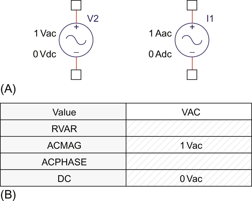
To perform an AC analysis, the independent voltage source VAC or current source IAC (Fig. 4.1A) from the source library is used. However, any independent voltage source which has an AC property attached to the part can be used as an input to the circuit. Fig. 4.1B shows the properties attached to the VAC part as displayed in the Property Editor.
By default, the magnitude of the VAC source is 1 V. In calculating the frequency response of a circuit, you are normally looking to calculate the gain and phase response of the circuit. Since the circuit gain is given by the ratio of Vout to Vin, setting Vin to 1 V, the gain or transfer function of the circuit will be equal to the output voltage, Vout.
4.1 Simulation Parameters
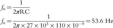
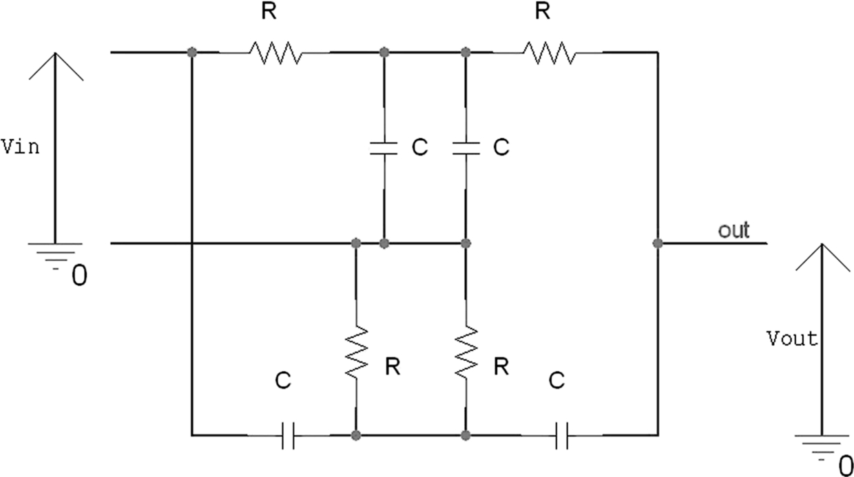
One example in which an AC analysis is used to determine the frequency response of a circuit is the notch filter, which attenuates a narrow band of unwanted frequencies—for instance, the removal of the mains frequency which can lead to unwanted “hum” in an audio amplifier. One common implementation of a twin T notch filter is shown in Fig. 4.2, where the notch frequency is given by:
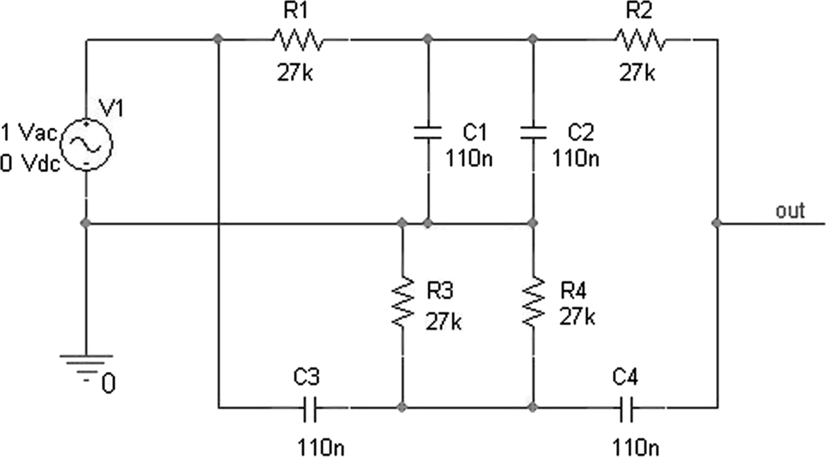
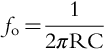
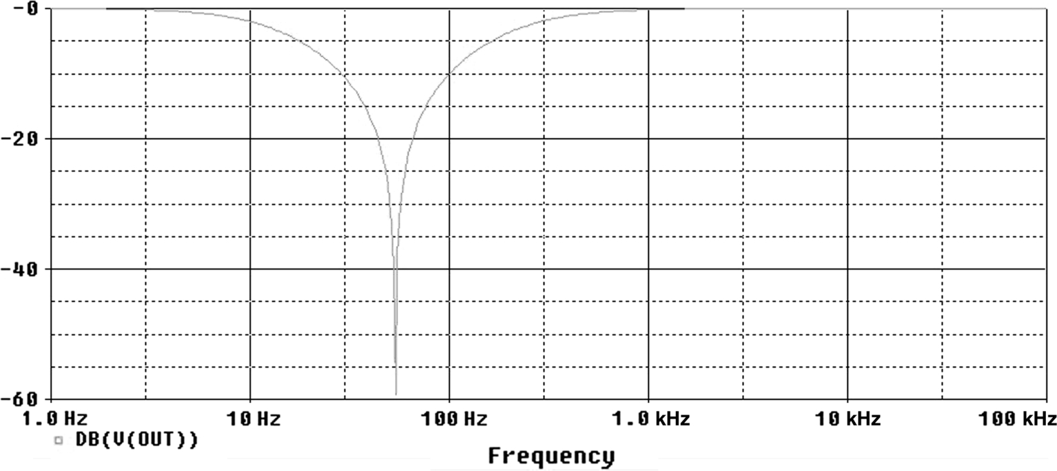
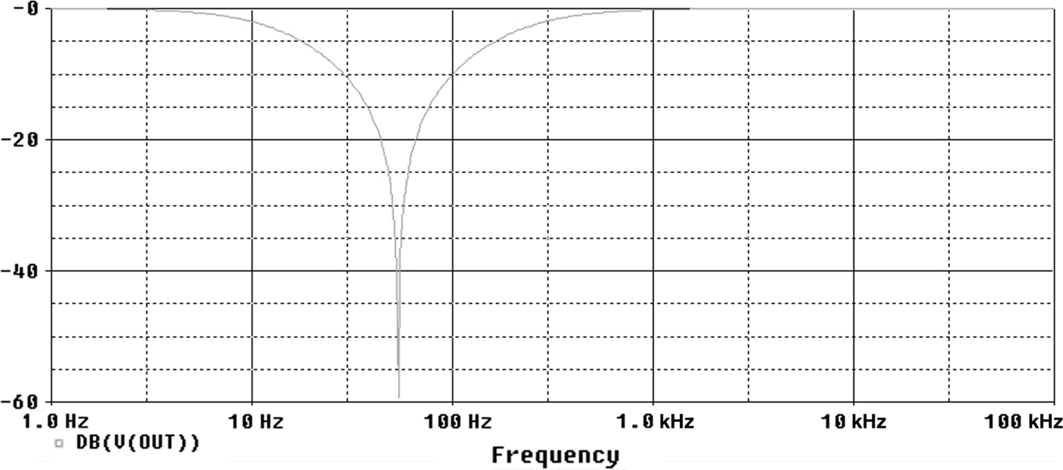
Fig. 4.3 shows the notch filter response of the circuit where the output is attenuated by − 60 dB at the notch frequency of 53 Hz.
To set up an AC analysis, a PSpice simulation profile needs to be created: PSpice > New Simulation Profile. In Fig. 4.4, the Analysis type is set to AC Sweep/Noise and has been set up for a logarithmic frequency sweep starting from 1 Hz to 100 kHz. You have the choice to sweep the frequency linearly over the whole range or logarithmically either in decades or in octaves. If you want to use a linear range, note that the Total Points is applied over the whole frequency range compared to, say, a decade range where the number of points applies to each decade.

4.2 AC Markers
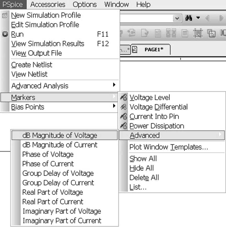
AC markers can be found under the PSpice > Markers > Advanced menu as shown in Fig. 4.5. These markers can be used to display dB magnitude, phase, group delay, and the real and imaginary parts of voltage and current. For example, a combination of these markers can be used for Bode and Nyquist plots.
4.3 Exercises
Exercise 1
Fig. 4.6 shows a passive twin T notch filter. You will create an AC sweep and plot the frequency response of the circuit.
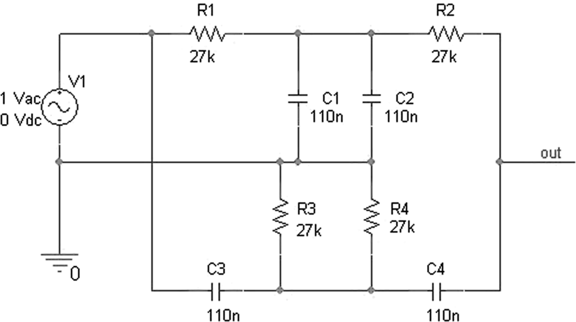
1. Draw the circuit of the notch filter in Fig. 4.6. The VAC source can be found in the source library.
2. Create a PSpice simulation profile to perform a logarithmic sweep from 1 Hz to 100 kHz in steps of 100 points per decade (Fig. 4.7).

3. Place a VdB voltage marker on the output node, “out.” This will automatically calculate the output voltage in dB: PSpice > Markers > Advanced > dB Magnitude of Voltage (Fig. 4.8).

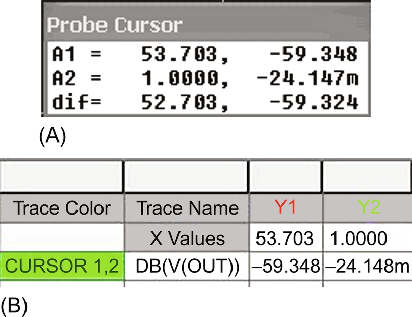
4. Run the simulation and you should see the notch filter response (Fig. 4.9). What we need to do now is to determine the frequency at the deepest part of the notch.
5. Turn on the cursor, Trace > Cursor > Display 
 and place the cursor at the bottom of the notch. For a more accurate reading, zoom in towards the bottom of the trace, View > Zoom > Area or use the icons
Alternatively, you can use one of the cursor functions, Trace > Cursor > Min  or
or  .
.
The Probe Cursor box will display a notch frequency 53.703 Hz with an attenuation of −59.348 dB as seen in Fig. 4.10, depending on which software version you are using. In both software versions, the Probe Cursor box can be positioned anywhere in the Probe screen.
6. Restore the Probe display to its original size, View > Zoom > Fit 
Select the trace name at the bottom of the display and press delete on the keyboard or select Trace > Delete all Traces. Now we are going to manually add the trace for the output voltage V(out).
7. Select Trace > Add Trace  and the Add Traces window will appear as shown in Fig. 4.11.

8. The Add Traces window displays all the data for all the nodes and devices in the circuit. Uncheck the boxes for Currents and Power and in the list of Simulation Output Variables, scroll down and select the V(out) variable.
Click on OK.
9. The V(out) trace will be displayed in the Probe trace window. However, what we want is the voltage in dB. Select the trace name V(out) and press the delete key to remove the trace.
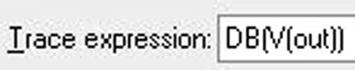
10. Select Trace > Add Trace and in the right-hand side of Add Traces under Analog Operators and Functions, select DB().
Then, as before, select V(out) from the list of Simulation Output Variables. At the bottom of the window in the Trace Expression box, you should see DB(V(out)). The DB function automatically calculates the DB of V(out). See Fig. 4.12.
Click on OK and you should see the trace shown in Fig. 4.13.
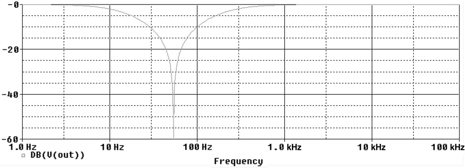
11. Repeat Step 5 to determine the depth of notch attenuation in dB.
4.3.1 Twin T notch filter
Fig. 4.14 shows the implementation of a notch filter which has a notch frequency given by
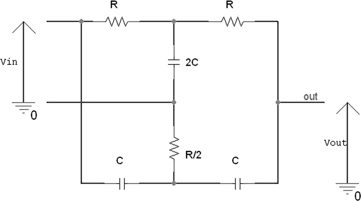
Using only one value of resistor and one value of capacitor, the circuit in Fig. 4.14 can be implemented as shown in Fig. 4.15.
The parallel combination of the two capacitors is given by:
The parallel combination of the resistors is given by:
which conforms to the circuit implementation shown in Fig. 4.14.
For the notch filter in Fig. 4.6, R = 27 kΩ and C = 110n. Therefore, using Eq. (4.1), the notch frequency is given by: