
Digital Simulation
Abstract
PSpice uses the same simulation engine for both analog and digital parts. Digital TTL and CMOS parts are modeled as subcircuits and include the common digital functions such as gates, registers, flip-flops, inverters, etc. Within each subcircuit, a digital primitive makes up the gate function (AND, OR, etc.) and defines the timing and interface specification for the gate function. Other digital devices include: delay lines, AtoD, DtoA, RAM, ROM, and Programmable Logic Arrays.
Keywords
Register; Inverter; Circuit; Simulation engine; Signals; Digital
PSpice uses the same simulation engine for both analog and digital parts. Digital TTL and CMOS parts are modeled as subcircuits and include the common digital functions such as gates, registers, flip-flops, inverters, etc. Within each subcircuit, a digital primitive makes up the gate function (AND, OR, etc.) and defines the timing and interface specification for the gate function. Other digital devices include: delay lines, AtoD, DtoA, RAM, ROM, and Programmable Logic Arrays.
18.1 Digital Device Models
A model definition for a 2-input CMOS NAND gate is shown here.
     ⁎ CD4011B    CMOS NAND GATE QUAD 2 INPUTS
     ⁎
     ⁎ The CMOS Integrated Circuits Data Book, 1983, RCA Solid State
     ⁎ tvh     09/29/89     Update interface and model names
     ⁎
     .subckt CD4011B  A B J
     +        optional: VDD =$G_CD4000_VDD VSS =$G_CD4000_VSS
     +        params: MNTYMXDLY = 0 IO_LEVEL = 0
     U1 nand(2) VDD VSS
     +         A B      J
     +   D_CD4011B IO_4000B MNTYMXDLY ={MNTYMXDLY} IO_LEVEL ={IO_LEVEL}
     .ends
The first five lines are comments giving a description of the part and a reference to the data source. On line six, is the subcircuit definition of the CD4011B with three pins A, B, and J. The global power supply is defined by VDD =$G_CD4000_VDD and VSS =$G_CD4000_VSS. The optional parameters, MNTYMXDLY = 0 defines the minimum, typical, and maximum delay and the IO_LEVEL which defines one of four AtoD or DtoA interface subcircuits if the digital device is connected to an analog device.
U1 defines a two input nand(2) primitive which has input terminals; VDD, VSS, A, B, and J. The “+” signifies a continuation to the next line. The next line (line 11) declares two models, the timing model, D_CD4011B, which defines the timing characteristics such as propagation delay, setup, and hold times and the I/O model, IO_4000B, which defines the loading and driving characteristics for the gate. Subcircuits always end with a “.ends” statement as in line 12. The model D_CD4011B can be found in the CD4000.lib and the model IO_4000B can be found in the dig_io.lib. More detailed information can be found in the PSpice reference manual.
18.2 Digital Circuits
Digital gates by default do not show their power supply pins because this would require a relatively large number of wires to connect all the gates to the power supply which would overcomplicate the circuit. Instead, TTL and CMOS devices are connected to global power supply nodes which are not displayed and by default are set to 5 V. Different power supplies can be set to accommodate the 3–18 V voltage supply range for CMOS devices. This will not affect the input thresholds and output drives for CMOS devices but the propagation delays will still be defined for a 5 V power supply. For accurate propagation delays, the timing models will have to be modified.
To set digital logic levels on IC pins, it is recommended to use digital HI and LO symbols from the Place > Power menu and to use digital PULLUP resistors from the dig_misc library to tie a pin high or low via a resistor. No Connect symbols, from the Place menu can be used to identify unconnected pins. Fig. 18.1 shows the respective Capture symbols and parts.

In Fig. 18.2, a digital clock signal is applied to the input of an 8-bit binary counter (U1A and U1B). In order to enable the counter, the CLR input is tied low by using a digital LO symbol. Each counter output is connected to an 8-bit bus using bus entry points, Place > Bus Entry, select the icon  or press E on the keyboard.
Each wire connected to a bus entry point has been labeled, D1, D2, etc. and the bus itself has a net name of D[8-1], the order of which is msb-lsb. The bus on the data inputs to U3 is also named as D[8-1] and will therefore be connected to the 8-bit bus. The bus can also be labeled as; D[7-0] or D[7..0], it is your preference. Only signals of the same type can be grouped together on a bus, mixed busses cannot be defined in Capture. However, in Probe, signals of different types can be collected together and displayed as a bus waveform. Markers can be placed on a bus as well as wires.
18.3 Digital Simulation Profile
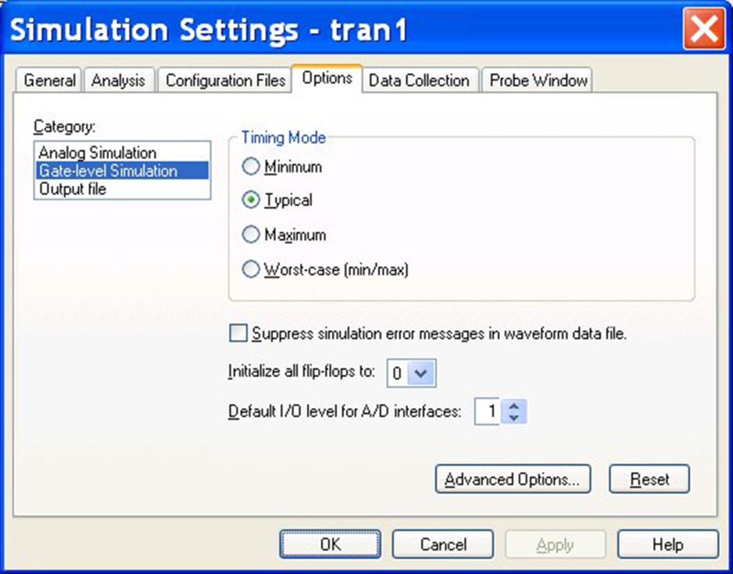
From version 17.2 onward, digital simulation options are presented differently. For pre 17.2 software releases, digital simulation options can be found in the simulation profile under the Options tab and selecting Category: > Gate-level Simulation as shown in Fig. 18.3. The Timing Mode option lets you select the Minimum, Typical, Maximum, or Worst-case timing characteristics for the digital devices. There are four I/O AtoD and DtoA interfaces you can select and most importantly of all, you can initialize all flip-flops to either X for do not care, logic 0 or logic 1. There is also the option to suppress simulation error messages as PSpice will report any digital timing hazards or timing violations.

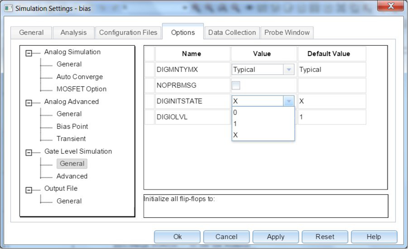
For post 17.2, the digital simulation options are found under Options > Gate Level Simulation > General, see Fig. 18.4. A description of each option is displayed in the bottom window when you click on the parameter name.
18.4 Displaying Digital Signals
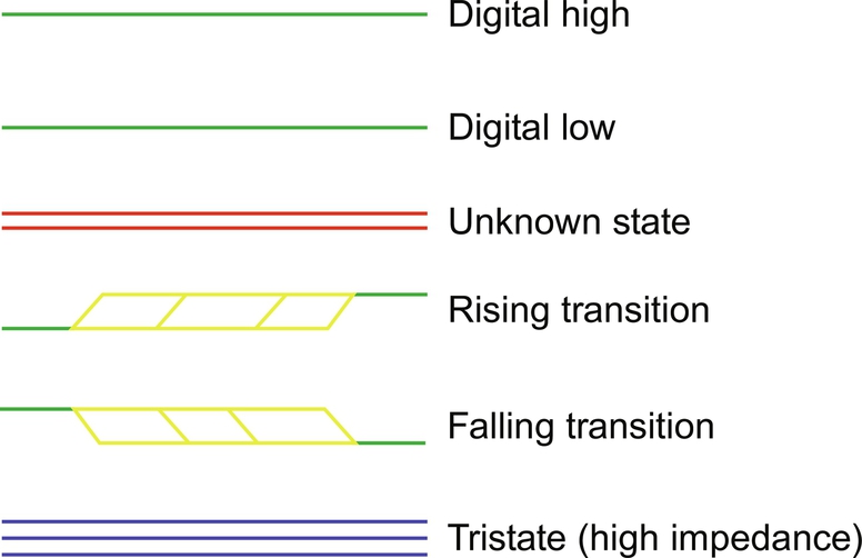
Digital signals are shown as either high or low logic levels. However, for regions of ambiguity where the transition time is not precisely known, the rising and falling transitions are shown in yellow as shown in Fig. 18.5. Unknown states are shown as two red lines and high impedance states are shown as three blue lines.
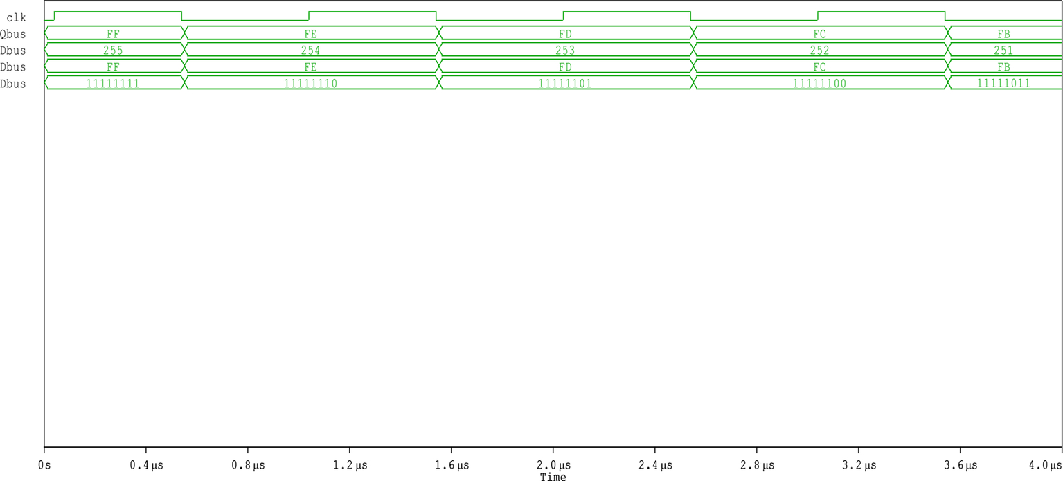
You can group digital signals together and displayed as a bus in the Probe window. The bus name can be created in the Trace Expression field in the Trace > Add Trace window. Up to 32 digital signals can be listed with the order msb to lsb with a radix of either; hexadecimal (default), decimal, octal, or binary. For example,
{D4 D3 D2 D1};myBus;d will display D4 to D1 (msb-lsb) labeled as myBus with decimal numbers
{WR RD CE};control;b will display bus control in binary
Fig. 18.6 shows a QB[8:1] bus shown by default in hexadecimal. The Dbus has been created from a collection of digital signals and is shown in hexadecimal, decimal, and binary.
18.5 Exercises
Exercise 1
You will verify the output sequence of a modulus 3 synchronous counter.
1. Create a project called Mod 3 Counter. Rename SCHEMATIC1 to counter and draw the modulus 3 synchronous counter in Fig. 18.7. The digital flip-flops and the OR gate are from the CD4000 library. The digital HI and LO symbols are from the Place menu or press “F” on the keyboard. The digital stimulus is digClock from the source library.

2. Name the nodes as shown. Place > Net Alias or press “N” on the keyboard.
3. You need to initialize the flip-flops to 0. If you have pre 17.2 software version, then follow step 3.1 otherwise for post 17.2 versions, follow step 3.2.
3.1 Set up a PSpice simulation profile for 100 μs and select Options > Category: Gate-level simulation and set Initialize all flip-flops to 0, see Fig. 18.8.
3.2 Set up a PSpice simulation profile for 100 μs and select Options > Gate Level Simulation > General. Set the Value for DIGINITSTATE to 0 from the pull down menu, see Fig. 18.9.

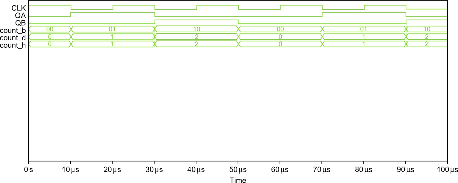
4. Place voltage markers on the CLK, QA, and QB nodes.
5. Run the simulation. The trace names will appear in the order that you placed the voltage probes. In Probe, rearrange the trace names such that the CLK is at the top, then QA and QB. This can be done by selectively cutting and pasting. Select CLK and press control-X which will delete the trace, then press control V to paste the trace name. Note that both traces QA and QB are initialized to logic 0.
6. Turn on the cursor and move the cursor along the waveforms. The corresponding logic levels should appear on the y-axis as in Fig. 18.10. Note that the output of the flip-flop only changes on the falling edge of the clock signal. The CD4027 flip-flops are negative edge triggered.

7. You will add a bus to show the binary count. Select Trace > Add and in the Trace Expression field enter
{QB,QA};count_b;b
and click on OK to display the binary count.
8. Select Trace > Add and in the Trace Expression field enter
{QB,QA};count_d;d
and click on OK to display the decimal count.
9. Select Trace > Add and in the Trace Expression field enter
{QB,QA};count_h;h
and click on OK to display the hexadecimal count.
10. Your Probe waveforms should resemble those shown in Fig. 18.11 which is that of a modulus 3 counter with a count sequence of 0,1,2,0,1,2,0, etc.
Exercise 2
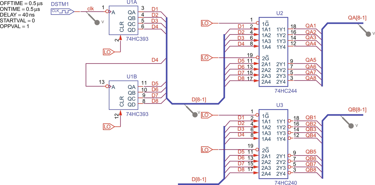
The circuit in Fig. 18.12 is an example of how to connect signals to a bus and how to select the different A and B sections of an IC. A clock signal is divided down by two 4-bit binary counters, U1A and U1B, and then passed to two octal buffers U2 and U3 via an 8 bit bus. U3 is an inverting octal buffer.
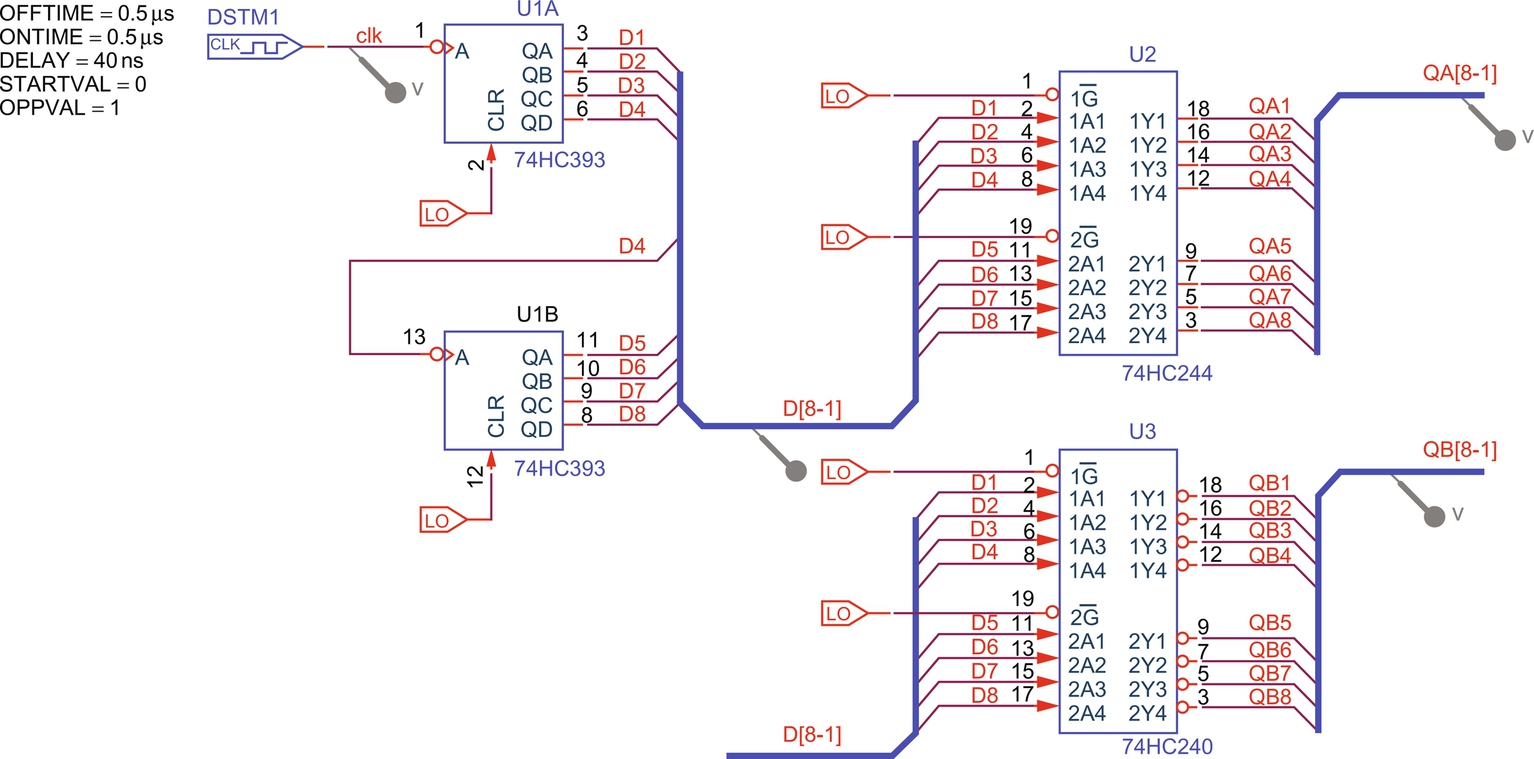
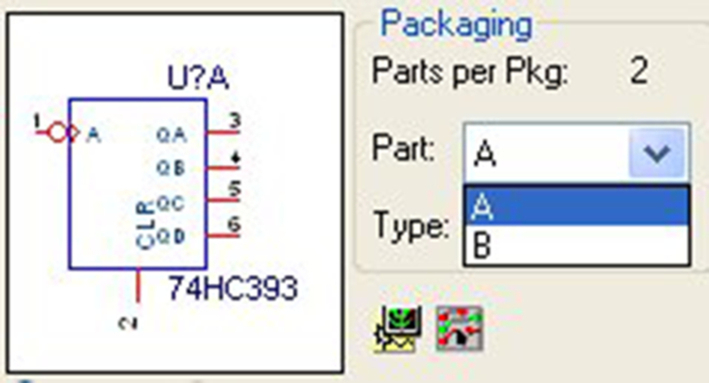
1. The 74HC393 has two identical sections designated A and B shown in the Packaging window in the Place Part menu in Fig. 18.13. When you select Part B, the pin numbers will change accordingly.
2. Place the parts for the circuit in Fig. 18.12 but do not connect the wires or bus yet. DSTM1 is a DigClock source from the source library and the HC devices can be found in the 74HC library. The HI and LO symbols are from the Place > Power menu.
3. Draw the busses in the circuit. To draw an angled bus, hold down the shift key and left mouse click to define the angle and then draw the bus.
4. Starting with U1A pin 3, place a bus entry on the bus as shown in Fig. 18.12. Draw a wire from the bus entry to pin 3 of U1A.
5. Select the wire and place a net alias (press N) labeled D1 on the wire. Press escape or rmb > End Mode.
6. Draw a selection box around the wire, net name, and bus entry point as shown in Fig. 18.14.

7. Hold the control key down, place the cursor on the wire, and drag it down so it connects to pin 4. The net name automatically increments to D2. With the wire still highlighted, press F4 twice and two more nets, D3 and D4 will appear.
Note
From release 16.3, there is now the option to Auto Wire two points Select Place > Auto Wire  , select two points and the wire is drawn automatically. Another new feature is the Place > Auto Wire > Connect to bus.
  You click on a connecting pin and then the bus such that the wire and bus entry will be connected automatically. You will also be prompted for the net name.
If you have release 16.3 or later go to (8) else continue to (9).
8. Select Place > Auto Wire > Connect to bus  and wire up the rest of the IC pins as in Fig. 18.12.
9. The busses are labeled the same as for wires using, Place Net > Alias. Make sure all three busses are labeled correctly, [msb-lsb].
10. As explained in Exercise 1, the presentation of the digital simulation options has changed between pre 17.2 and post 17.2 releases. For pre 17.2 follow step 10.1 otherwise for post 17.2 releases, follow step 10.2.
10.1 Set up a simulation profile for a transient analysis with a run to time of 10 μs. Select Options > Category: Gate-level simulation and set Initialize all flip-flops to 0, see Fig. 18.15.

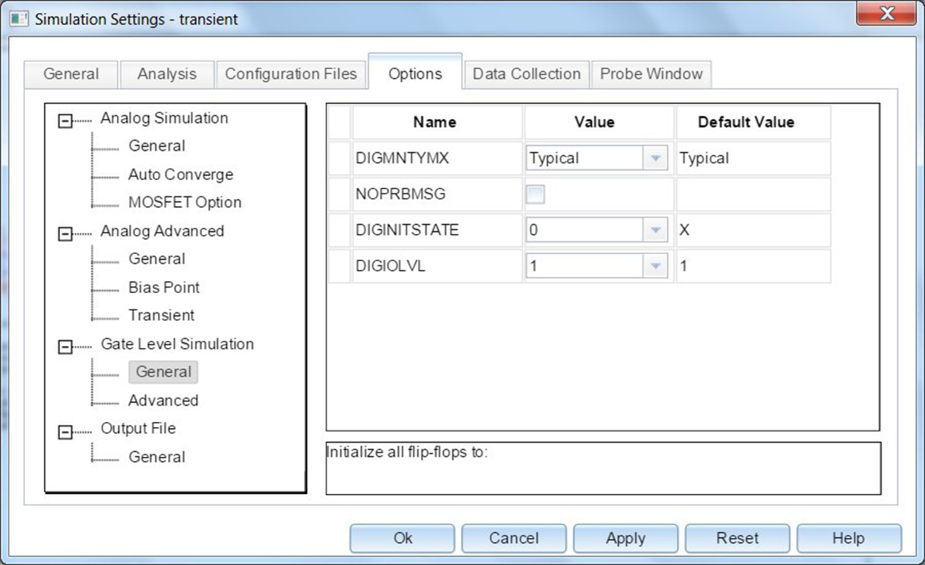
10.2 Set up a simulation profile for a transient analysis with a run to time of 10 μs. Select Options > Gate Level Simulation > General. Set the Value for DIGINITSTATE to 0 from the pull down menu, see Fig. 18.16.
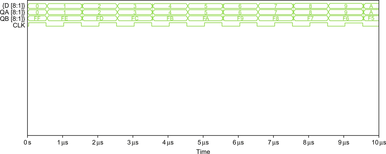
11. Place voltage markers on each bus as shown and run the simulation.
12. You should see the count increase for bus D[8-1] and QA[8-1]. As U3 is an inverting buffer, the count for QB[8-1] will start at FF and decrease accordingly. Compare your waveforms with those shown in Fig. 18.17.
13. Delete all the traces, Trace > Delete All Traces.
14. Select Trace > Add Trace. On the right hand side in the Functions or Macros, select the curly brackets {} the Trace Expression box will contain {} with the cursor sitting in the middle waiting for you to select a trace variable name.
15. Select D4 followed by D3, D2, and D1. Add the following text to the expression and click on OK.
16. Create a bus called nibble consisting of QA4, QA3, QA2, and QA1 and display the bus in binary.
You should see the waveforms as in Fig. 18.18.

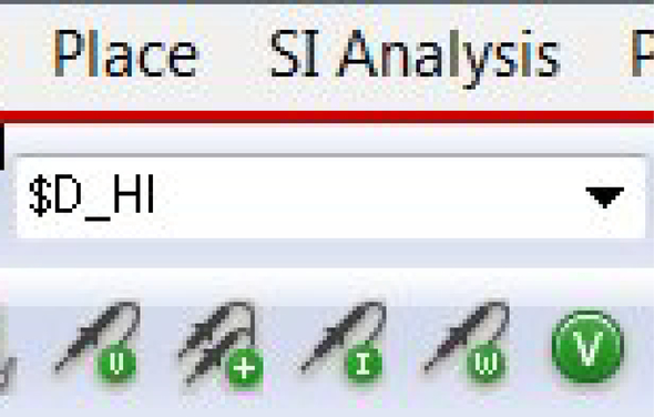
17. In Capture disable U2 by setting the enable pins ![]() , 1 and 19 high by using a $D_HI symbol from Place > Power. Run the simulation.
, 1 and 19 high by using a $D_HI symbol from Place > Power. Run the simulation.
Tip
Select the $D_HI symbol from the most recently placed part list, see Fig. 18.19. If the symbol is not in the pull down menu, type $D_HI in the box and press return.
19. The trace for QA[8-1] is displayed with a Z inside indicating a high impedance tri-state output, see Fig. 18.20.

Exercise 3
PSpice reports and plots timing violations relating to setup times, hold times, and minimum pulse width. By decreasing the clock pulse width we can investigate the reporting of these errors.
1. Change the clock OFFTIME to 0.01 μs and ONTIME to 0.01 μs.
2. Reduce the simulation time from 10 to 1 μs.
3. Run the simulation.
4. The Simulation Message window will appear as shown in Fig. 18.21.
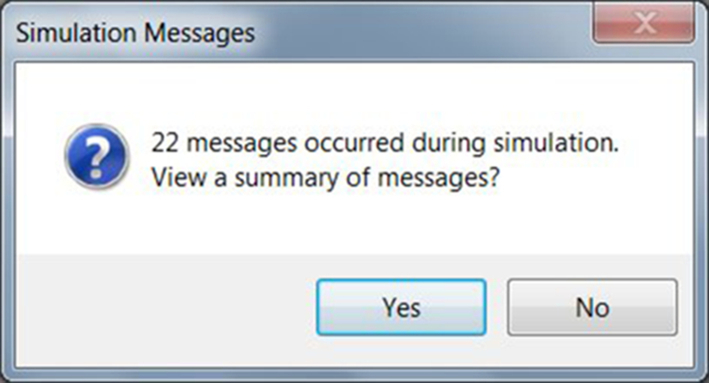
5. Click on Yes and you will see a list of Warnings (Fig. 18.22).

6. The Minimum Severity Level pull down menu lists severity levels for Fatal, Serious, Warning, and Info. For Fatal severity, the simulation stops. Leave the level on Warning and click on Plot.
7. The violation information displayed gives the time at which the violation occurred and with which device. The message not only gives you the measured violation timing value but also the specified timing value. PSpice also plots the occurrence of the violated timing waveforms.
Selecting each Time-Message will open up a new Probe plot window. All the reported violations can be viewed in the output file, VIEW > Output File.
DIGITAL Message ID#1 (WARNING):
WIDTH/MIN-HIGH Violation at time 50 ns
Device: X_U1A.UHC393DLY
Minimum high WIDTH = 20 ns
NODE: X_U1A.A, measured WIDTH = 10 ns