Test Benches
Abstract
From version 16.5, one can use the Partial Design Feature, which uses test benches to allow users to define those components that are used only for simulations. Users can also selectively partition designs for different simulation profiles and build up designs using circuits from other projects. Using test benches is very useful when users have a design that has been put together from a collection of circuits from other projects, as it will allow them to test the functionality of each individual circuit as they build up to the complete design. When a test bench is created, a Test Bench folder, which contains all the design schematics is added to the bottom of the Project Manager. All the components in all the schematics in the Test Bench folder are grayed out. Users then selectively “activate” those parts that are required for simulation and add parts such as voltage sources and load resistors. Parts can be deselected and selected either from the master design or from the created test benches. When users create a test bench, another design folder is created in the project folder. The Schematic-to-Schematic (SVS) utility compares test bench designs to the master design such that the master design can be updated with modified component values.
Keywords
Simulation; Test bench; Circuit; Block; Voltage; Resistors
Normally, when you run simulations on a circuit, you add, for example, voltage sources and load resistors to test the circuit. You may even remove components from a circuit in order to run simulations. However, once the simulations are complete, these add-on components will have to be removed and any deleted components restored.
Before version 16.5, you could add a PSpiceOnly property to the parts that are only used for simulation and therefore these parts would not be included, for example, in the printed circuit board (PCB) netlist. From version 16.5, you can use the Partial Design Feature, which uses test benches to allow you to define those components that are used only for simulations. You can also selectively partition designs for different simulation profiles and build up designs using circuits from other projects. Using test benches is very useful when you have a design that has been put together from a collection of circuits from other projects, as it will allow you to test the functionality of each individual circuit as you build up to the complete design.
When you create a test bench, a Test Bench folder, which contains all the design schematics, is added to the bottom of the Project Manager. All the components in all the schematics in the Test Bench folder will be grayed out. You then selectively “activate” those parts that are required for simulation and add parts such as voltage sources and load resistors. Parts can be deselected and selected either from the master design or from the created test benches.
When you create a test bench, another design folder is created in the project folder. The project folder will then contain two folders:
< project name >-TBFiles
The Schematic to Schematic (SVS) utility will compare test bench designs to the master design such that the master design can be updated with modified component values.
22.1 Selection of Test Bench Parts
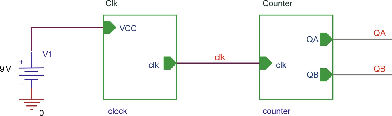
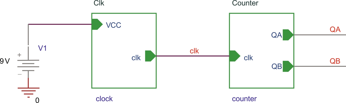
As mentioned previously, there will be two design folders, the master design and the test bench design. You can select those parts required for simulation from either the master design or the test bench design depending on which design you have open, but ultimately you will be simulating the test bench design. For example, Fig. 22.1 shows a hierarchical design of a digital counter which contains a clock oscillator and a modulus-3 counter.
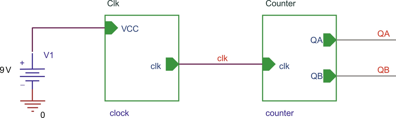
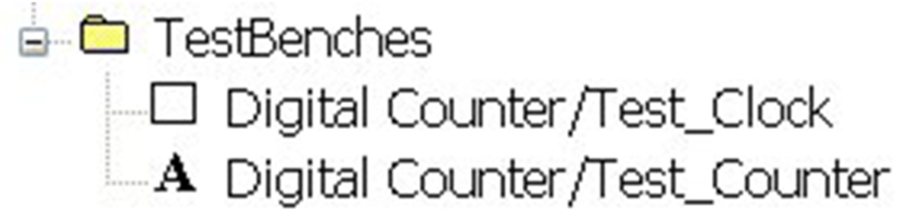
Both blocks will be tested separately using two test benches, Test_Clock and Test_Counter. Initially, all schematic parts are grayed out. From the master design you create a test bench by selecting Tools > Test Bench > Create Test Bench and name the test bench, which is added to the master design Project Manager. You can create multiple test benches, but only one test bench will be active, denoted by an A in front of the test bench name. You can then select parts from the master design and add to the active test bench by rmb > Add Part(s) To Active Testbench. In Fig. 22.2, the Test_Counter is the active test bench.

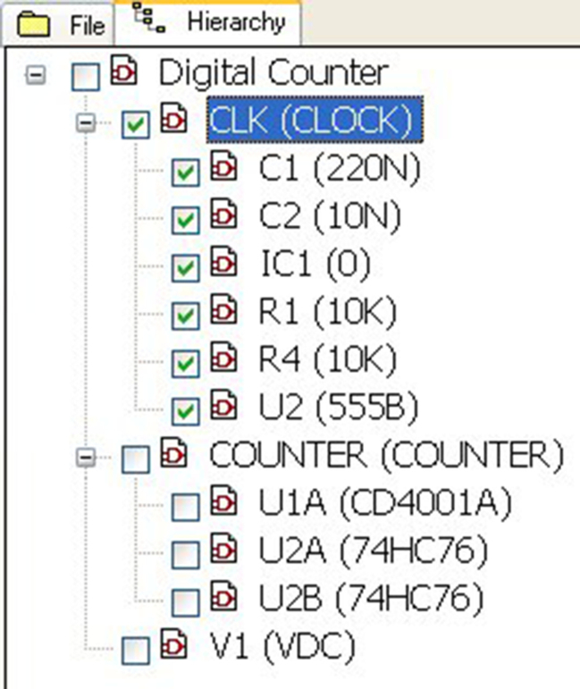
From the master design you can also select and deselect parts using the hierarchy tab in the Project Manager. Fig. 22.3 shows the hierarchy tab of the master design Project Manager. In this example, only the parts in the Clock hierarchical block will be selected. All the other parts in the design will be grayed out.
Alternatively, you can add and remove parts from a test bench design. In the above example, if you open the Test_Clock/Test Bench > clock schematic, you can select parts and then rmb > Test Bench > Add Part(s) To Self or Remove Part(s) From Self (Fig. 22.4), where Self refers to the active Test_Clock/Test Bench.

22.2 Unconnected Floating Nets
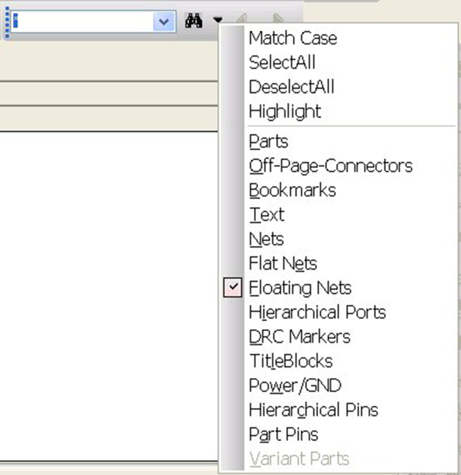
Adding and removing parts in a design can lead to unconnected wires, resulting in floating node errors. As discussed in Chapter 2, all nodes must have a DC path to ground. You can search for floating nets using the Text to Search Box, which presents a list of searchable objects (Fig. 22.5), one of which is floating nets.
Floating nets must be resolved, otherwise the simulation will not proceed. Sometimes, all that is required is to connect a resistor between the floating net and ground to provide the DC path to ground.
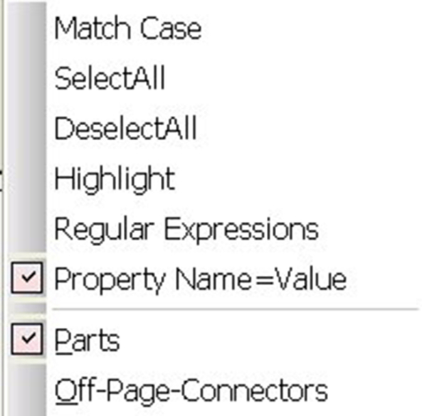
In 16.6 two advanced search features have been added as shown in Fig. 22.6. Regular Expressions and Property Name = Value.

Property Name = Value requires the full Property name whereas for Value, the ∗ wildcard and character? marks can be used. For example in the Digital Counter, to find all ICs, you select Property Name = Value as shown in Fig. 22.7.
Then enter, Part Reference = U ∗.  To be more specific in searching only for digital 74 series type 76 JK flip flops ICs, regardless of the technology, i.e. LS, HC, AC etc., then you can enter; Value = 74??76.
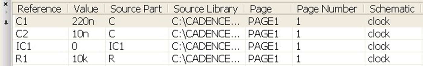
 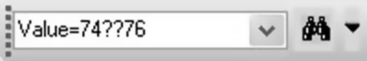 The Regular Expression offers more flexibility in providing conditional searching for strings, i.e. you can specify a range of values or can be selective in using AND or OR (|) functions. For example, if you want to find the first resistors R1,R2 OR the first capacitors C1, C2 in the Digital Counter, then you could enter; Part Reference =(C | R)[1-2]. Note that both the Regular Expression and Property Name = Value are both selected.
  The result of the search finds R1, C1, C2 and IC1, the initial condition part as shown in Fig. 22.8.
22.3 Comparing and Updating Differences Between the Master Design and Test Bench Designs
Design differences between the master design and test bench designs can be viewed in the SVS utility, which displays the differences using a color-coded system to highlight missing parts (red), unmatched parts (yellow) and matched parts (white). In Fig. 22.9, the test bench design is shown on the left-hand side and the master design on the right-hand side. The test bench clock schematic contains an extra capacitor C3, shown in red, and a different value for R4.

You can update the test bench design with modified component values to the master design by selecting the Accept Left icon  . However, only modified values will be updated to the master design. In the example above, if you check the Value box for R4 in the left-hand panel, the modified value for R4 will be updated from the test bench to the master design. The extra capacitor C3 will not be updated to the master design. In addition, the master design cannot be updated if there are missing parts, so removed parts in test benches will not be removed from the master design.
22.4 Exercises
Exercise 1
Fig. 22.10 shows the hierarchical Digital Counter design from Chapter 20, Exercise 5.
You will now create a Test_Clock Test Bench to simulate and verify the performance of the clock oscillator only. In the master design, you will only add clock parts to the active test bench by selecting those parts in the Hierarchy tab in the master design Project Manager.
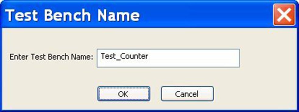
1. Select Digital Counter.dsn and from the top toolbar select Tools > Test Bench > Create Test Bench. Name the test bench Test_Clock, as shown in Fig. 22.11. Click on OK and click on OK again if prompted to save the design.
The Test_Clock test bench will be placed at the bottom of the Project Manager in the TestBenches folder (Fig. 22.12).

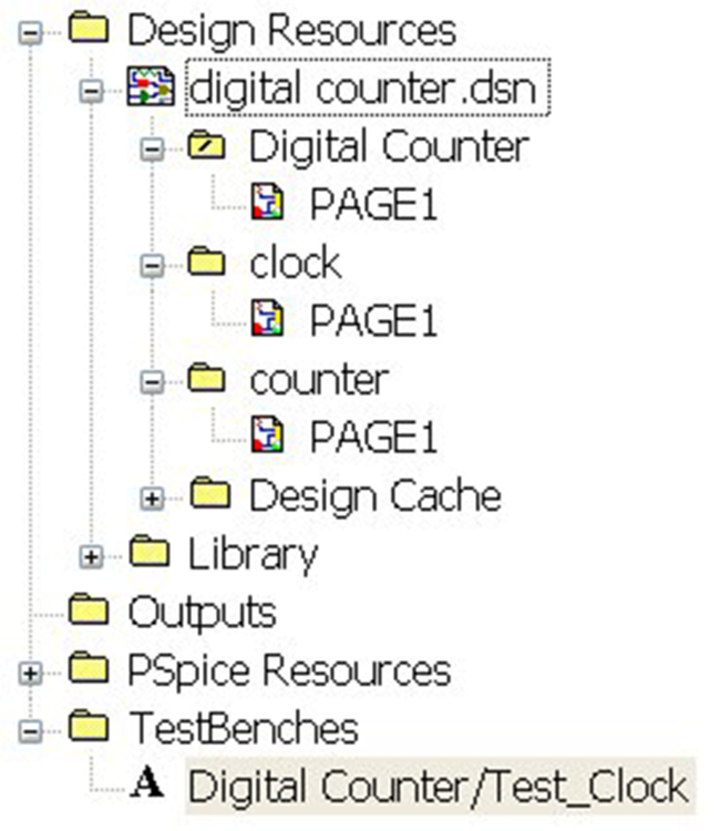
2. In the TestBenches folder, double click on Digital Counter/Test_Clock, which will open the Test_Clock.dsn design.
3. In the Test_Clock Project Manager, double click on Test_Clock.dsn and open the counter Page1 schematic. You will see that all the components are grayed out. Close the schematic page.
4. Still in the Test_Clock Project Manager, open the clock schematic and you will also see all the components grayed out.
You will now activate the clock components in the Test_Clock test bench from the master design.
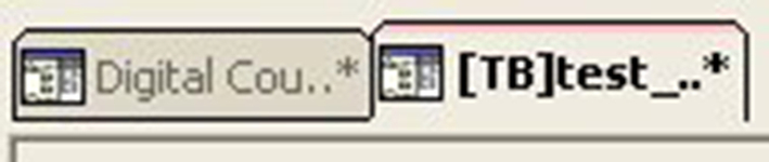
5. Select the master design Project Manager by either selecting the Digital Counter tab above the schematics (Fig. 22.13) or selecting Window > Digital Counter. It may be easier to place the master and test bench designs side by side.
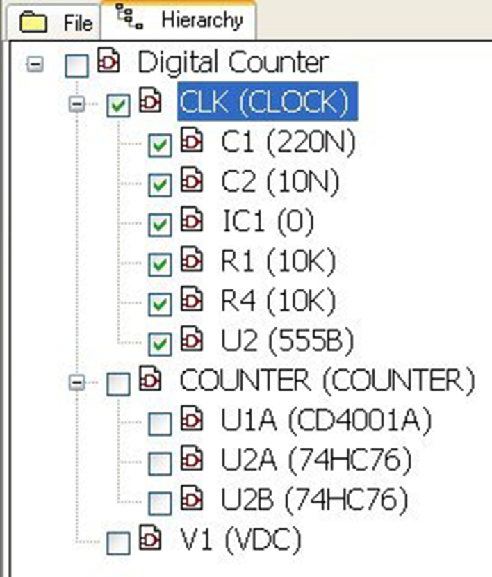
6. In the master design (Digital Counter) Project Manager, click on the Hierarchy tab to display the hierarchical design. Expand Digital Counter and Clock if not already expanded and check all the parts for Clock as shown in Fig. 22.14. Click on the File tab.
7. In the TestBenches folder, double click on the Digital Counter/Test_Clock test bench to activate the Test_Clock test bench Project Manager and open the clock schematic to check that all parts are active (nongray). Close and save the schematic.
8. Still in the Test_Clock Project Manager, open the Digital Counter schematic page as shown in Fig. 22.15.
The voltage source V1 is still grayed out. Draw a box around V1, the connecting wires and the 0 V symbol and rmb > TestBench > Add Part(s) To Self (Fig. 22.16).
Now that only the clock oscillator circuit is active; you need to search for unconnected nets in the Test_Clock test bench. Make sure the Searchmenu is displayed: select View > Toolbar > Search.

9. Highlight the Test_Clock.dsn and select, from the top toolbar, the pull-down menu to the right of the Binocular  , which is next to the Text to Search Box (Fig. 22.17).
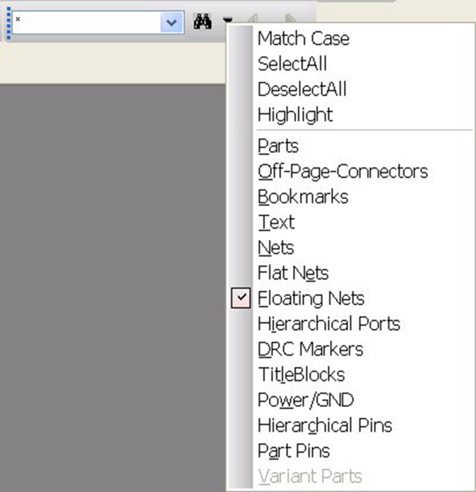
10. Click on DeselectAll. Next, select Floating Nets and then click on the Binocular icon  .
.
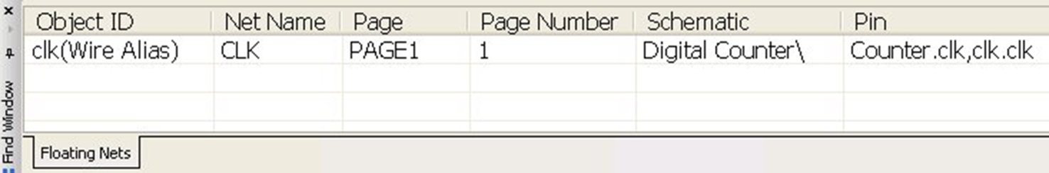
The Find window at the bottom of the screen, below the schematic, reports a floating net on the clk net (Fig. 22.18).
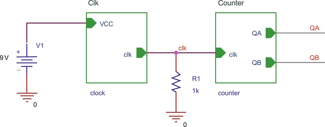
11. Place a 1k resistor from the clk net to ground as shown in Fig. 22.19. This provides a DC path to ground for the clk net.
12. Create a PSpice simulation profile for a transient analysis with a run to time of 20 ms. Do not exit the simulation profile.
You will need to initialize all flip-flops to 0. Select the Options tab > Gate-level Simulation and initialize all flips-flops to 0.
13. Place a voltage marker on the clk net and run the simulation.
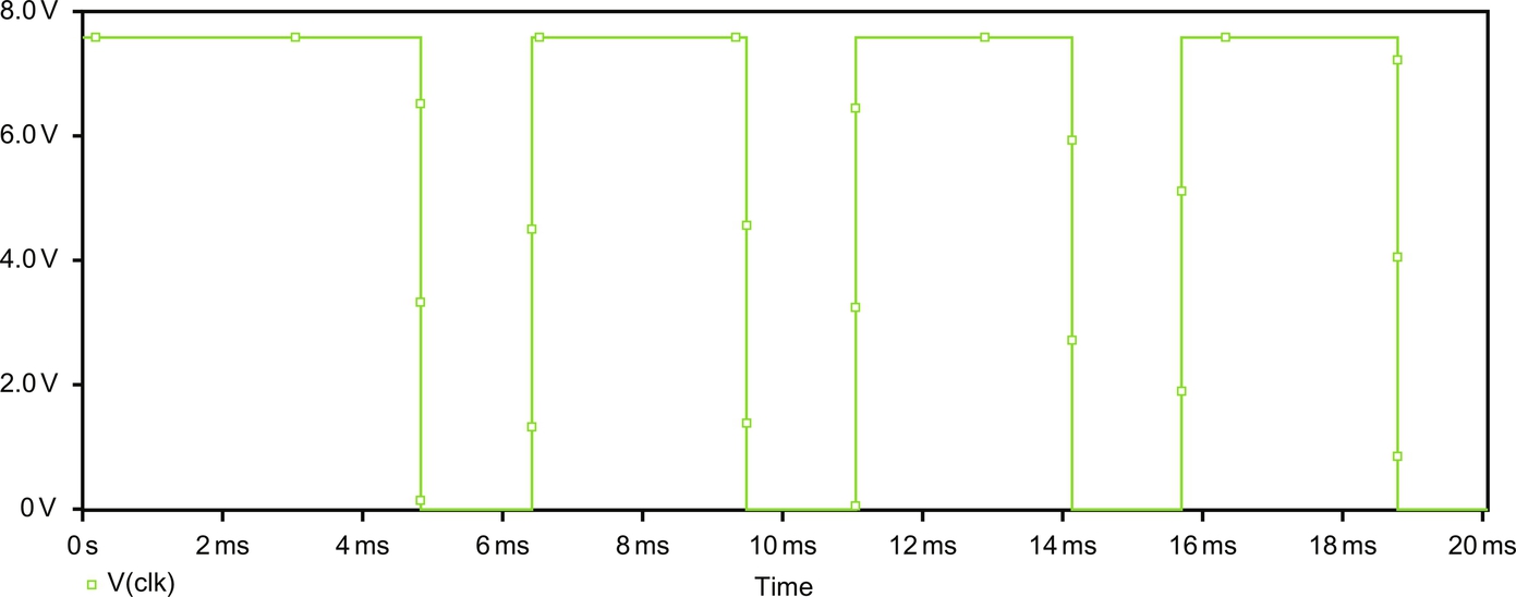
14. You should see the clock output waveform as in Fig. 22.20, which has a frequency of 216 Hz.
15. Double click on the clock hierarchical block to open the clock schematic and place another 220 nF in parallel with C1. Change the value of R4 in Fig. 20.42 to 6k8 and rerun the simulation. The clock frequency will now be 138 Hz. Close and save the clock schematic.
Now you will verify the operation of the counter circuit, but this time you will select the active parts from an active Test Bench. The counter parts will be added to the active Test Bench and the clock parts will be removed from the active Test Bench.
16. Open the Project Manager for the Digital Counter (master design).
17. Highlight the Digital Counter.dsn and select Tools > Test Bench > Create Test Bench. Name the test bench Test_Counter (Fig. 22.21).
18. There will be two test benches in the master design counter, as shown in Fig. 22.22. The A in front of the Test Counter test bench represents the active test bench. You can make a test bench active by rmb > Make Active.
19. Double click on the Test_Counter test bench to open the Test_Counter design
20. Double click on Test_Counter.dsn and open the Digital Counter schematic Page1.
21. Draw a box around the clock hierarchical block, V1 and the 0V symbol and then rmb > Remove Part(s) From Self (Fig. 22.23).

22. Draw a box around the counter hierarchical block and make sure the clk, QA and QB nets are also selected; rmb > TestBench > Add Part(s) To Self (Fig. 22.24).

23. Repeat Step 17 and check for floating nets. The QA and QB should be reported as floating. These are digital output nodes and therefore do not require a DC path to ground. Ignore the warning.
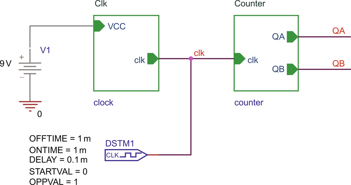
24. Add a DigClock source from the source library and set its parameters as shown in Fig. 22.25.
25. Create a PSpice simulation profile for a transient analysis with a run to time of 20 ms. Do not exit the simulation profile.
Do not forget to initialize all flip-flops to 0. Select the Options tab > Gate-levelSimulation and initialize all flips-flops to 0.
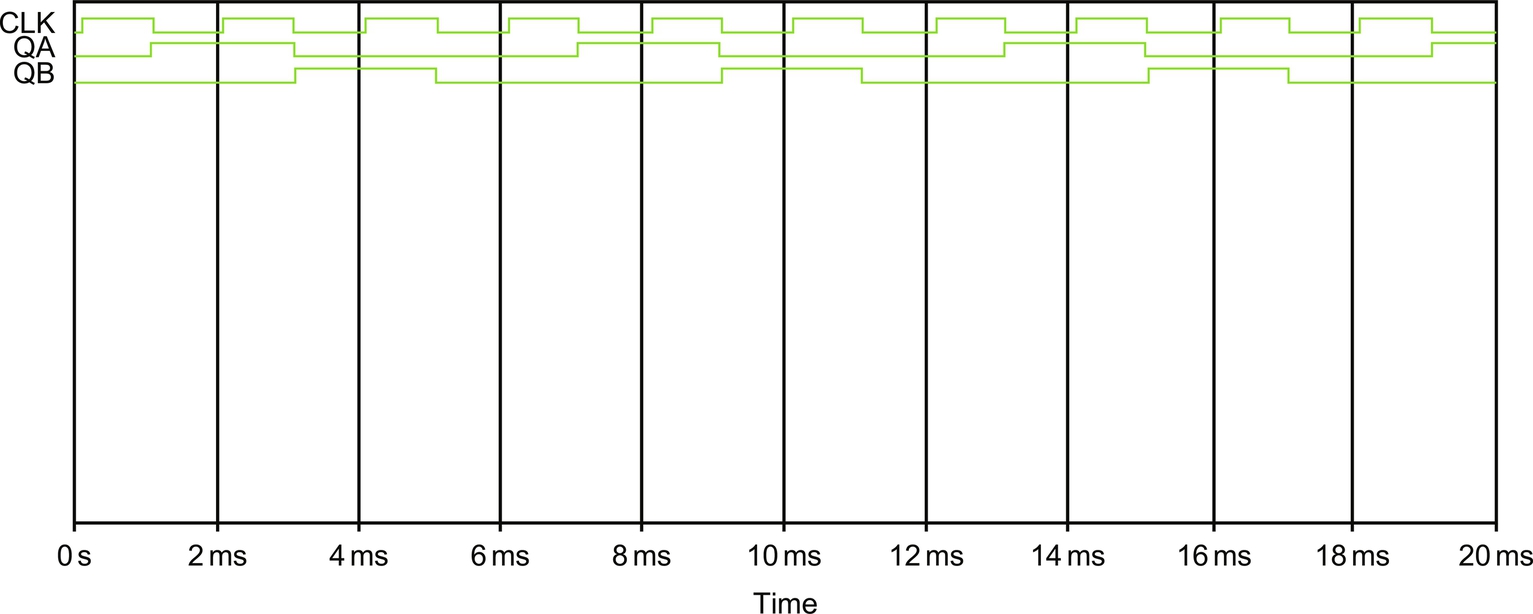
26. Place voltage markers on QA and QB and run the simulation. You should see the circuit response as shown in Fig. 22.26.
Exercise 2
After the test bench simulation testing, any differences between the master and test bench designs, component additions, removals and change in component values can be highlighted.
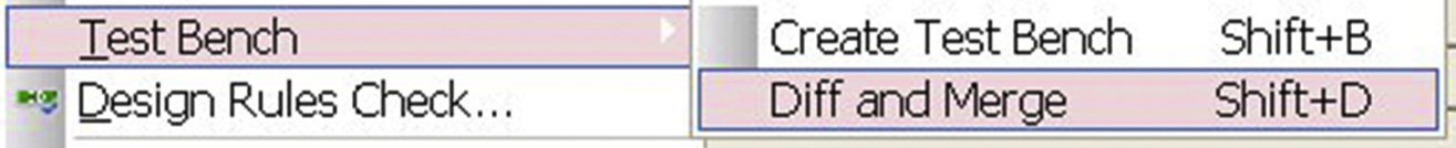
1. In the master design, highlight Digital Counter.dsn and select Tools > TestBench > Diff and Merge (Fig. 22.27).
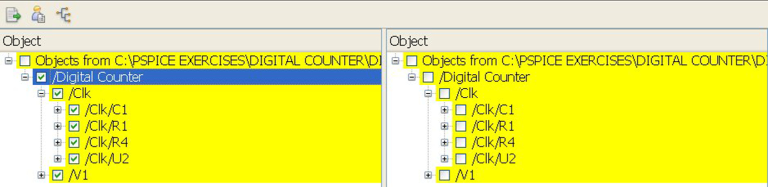
2. In the SVS window, the test bench is on the left-hand side panel and the master design on the right-hand side panel. In the left panel, expand the /Clk as shown in Fig. 22.28.
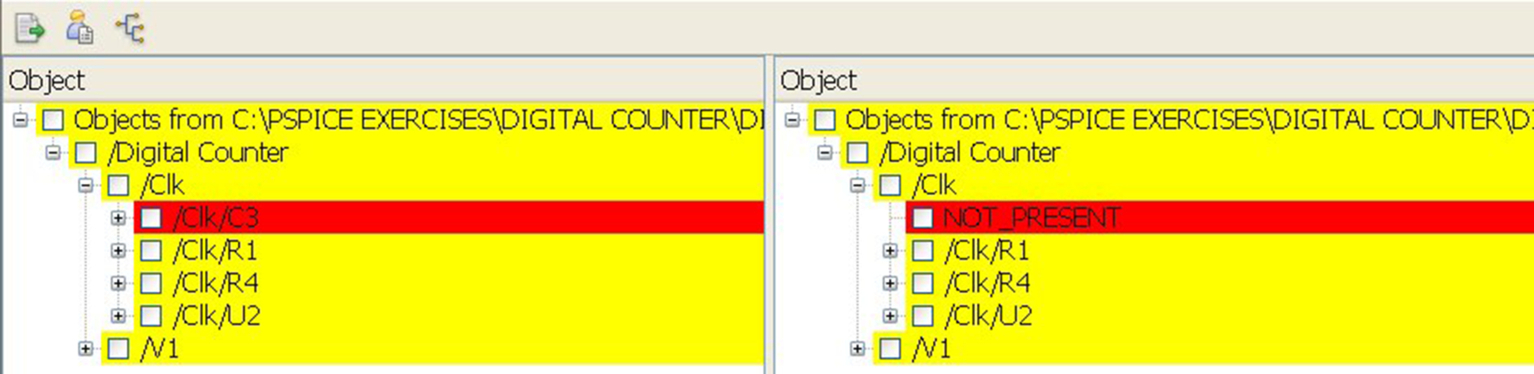
Yellow indicates the design differences between the Test_Clock test bench and the master design, which allows you to update any modified values to the master design.
The extra capacitor in the clock circuit has been highlighted in red and shown as NOT_PRESENT in the master design.
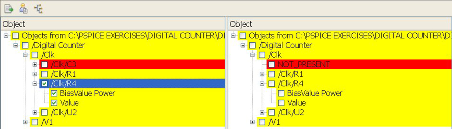
3. Expand /Clk/R4 and you will see a Value box displayed for both the Test_Clock test bench and the master design. This allows you to decide which value of R4 to accept by checking the appropriate Value box.
The modified value for R4 will be updated to the master design.
Check the /Clk/R4 box as shown in Fig. 22.29. The BiasValue Power is a measurement and is not important for this exercise.
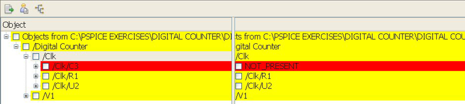
4. To update the master design with the new value for R4, click on the Accept Left icon  ; as there is no longer a difference between R4 in the test bench and the master design, R4 will not be displayed in the SVS window (Fig. 22.30).
If you tried to update the extra capacitor, C3, the session log will display the warning message:
WARNING(ORCAP-37003): Could not add object ’/Clk/C3’ at the target design, as this operation is not supported
5. Close the SVS utility and open the Test_Clock test bench design.
6. Open the clock schematic.
7. Delete the capacitor C3 and modify the value of C1 to 470n.
8. Save and close the clock schematic.
9. Open the master design and highlight the Digital Counter.dsn. Check for design differences: Tools > Test Bench > Diff and Merge.
10. The SVS window will show only value differences between the designs highlighted in yellow. Check the /Digital Counter box as in Fig. 22.31 and click on the Accept Left icon  .
.
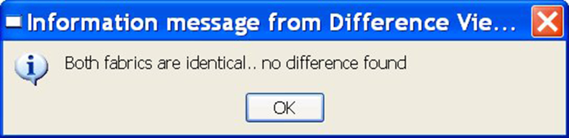
11. The message window will appear, reporting no differences (Fig. 22.32).
The SVS window will appear as shown in Fig. 22.33 with no entries.