DC Analysis
Keywords
Voltage; Model parameter; Message; Probe; Bias point; Resistance
The DC analysis calculates the circuit's bias point over a range of values when sweeping a voltage or current source, temperature, a global parameter, or a model parameter. The swept value can increase in a linear or a logarithmic range or can be a list of increasing values.
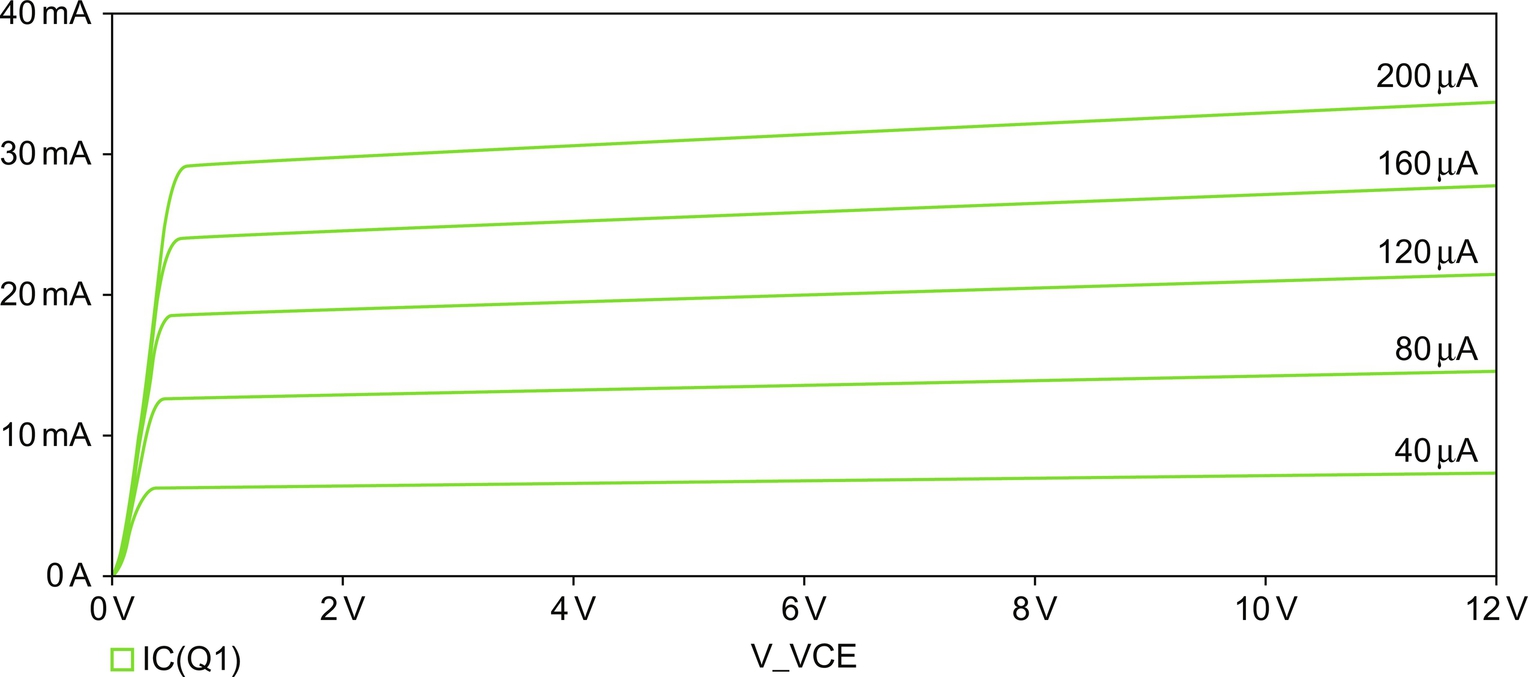
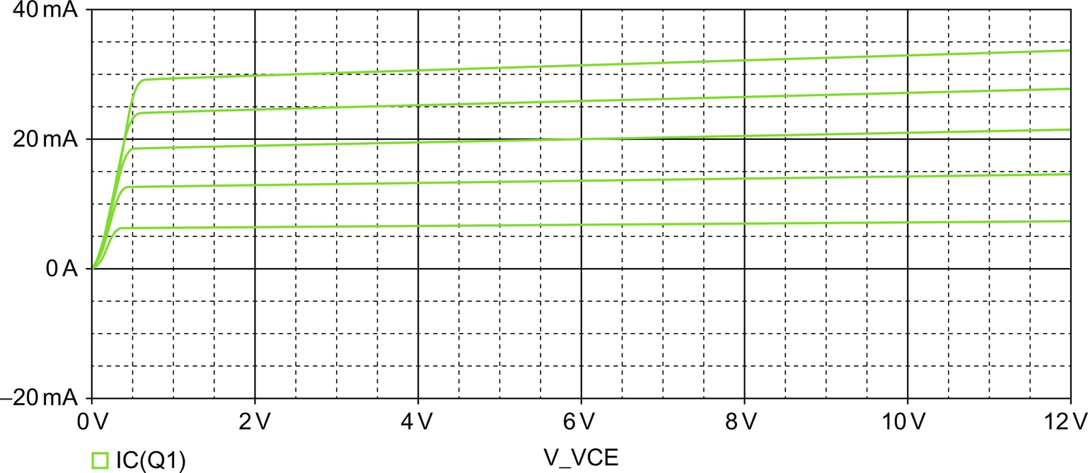
This is useful, for example, if you want to see the circuit response for a change in the supply voltage or to see how a change in a resistor value affects the circuit response. The DC Sweep also allows for nested sweeps such that one of two variables is kept constant while sweeping the other variable. For example, the characteristic transistor IC − VCE curve plots the collector current against the collector-emitter voltage for fixed values of base current. The DC Sweep will then contain two variables, the collector-emitter voltage VCE and the base current IB. The base current is the secondary sweep, while the VCE is the primary sweep. The collector current IC is recorded by successive voltage sweeps of the collector-emitter voltage VCE for stepped values of base current producing a series of curves as shown in Fig. 3.1.

3.1 DC Voltage Sweep
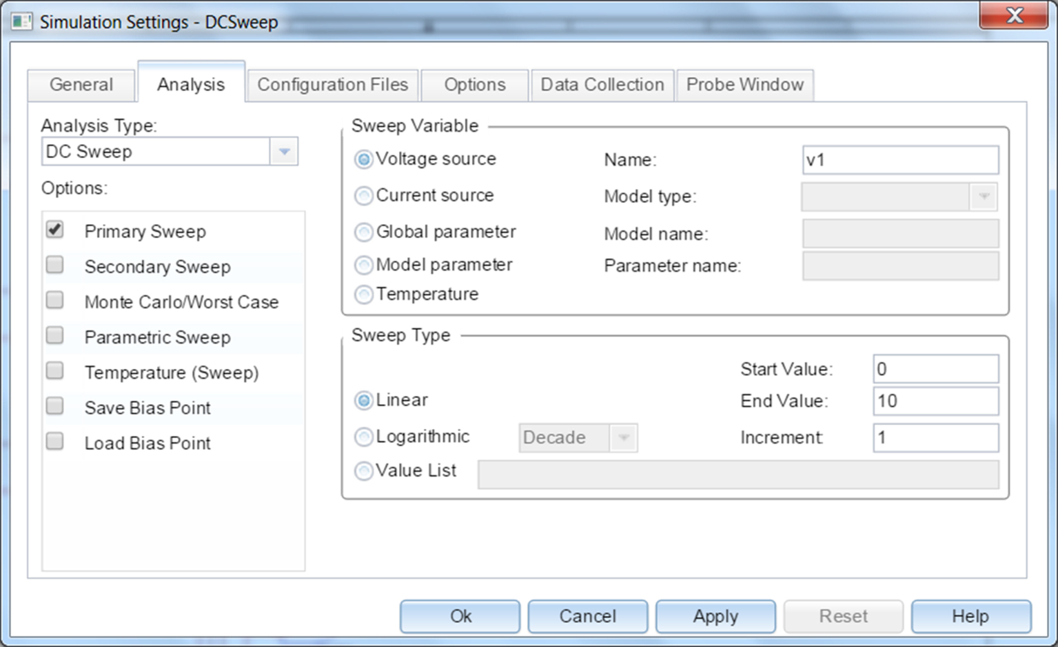
As with other analysis types, a PSpice simulation profile needs to be created. For a DC Sweep Analysis, select PSpice > New Simulation Profile and select DC Sweep for the Analysis type. Make sure the Sweep Variable is set to Voltage source. The Name is the reference designator for the voltage source which in this case is V1. The sweep type is set to Linear, starting from 0 to 10 V in steps of 1 V. You can also enter a list of voltages in the Value list, for example; 1 2 4 5 99 100 as long as the voltages are increasing in value. Fig. 3.2 shows the simulation profile for a DC linear sweep of V1 from 0 to 10 V in steps of 1 V.
3.2 Markers
Markers are used to record the voltages on nodes or currents through components and are accessed from the PSpice menu. They enable data to be automatically displayed as a waveform in the PSpice waveform viewer which is known as the Probe window. To add markers select, PSpice > Markers and then you have a choice of placing current, voltage, or differential voltage markers as shown in Fig. 3.3. The Advanced markers are primarily used with an AC analysis and will be covered in the chapter on AC analysis.
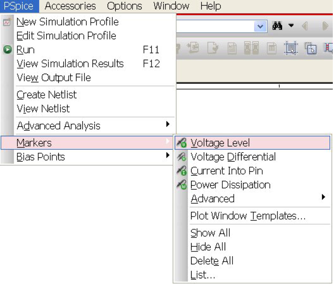
Fig. 3.4A shows the icons for the markers in version 16.2 and Fig. 3.4B the markers from 16.3 versions onwards.

Voltage markers are placed on wires whereas current markers must be placed on a component pin. A message (Fig. 3.5) will appear if you try to place a current marker on a wire instead of a component pin. The component pin is a different color to a wire and in version 16.3, component pins are noticeably thinner than the connecting wires. For power markers, the markers are placed on the body of the device.

Fig. 3.6 shows the addition of two voltage markers on the resistor circuit which will record the voltage at nodes “in” and “out” respectively and automatically display their voltage traces in the PSpice Probe waveform window.

When the simulation is run, PSpice will launch and Probe, will plot the two voltage traces at nodes in and out. The x-axis is the swept voltage V(in) and the y-axis is the resultant voltage V(out). Note that the respective traces have the same color as the markers placed in the circuit. See Figs. 3.6 and 3.7.

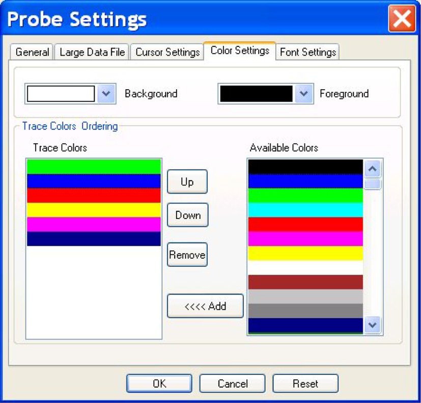
In release 16.3, you can now change the Probe background color which by default is black. From the top tool bar in PSpice, select, Tools > Options > Color Settings.
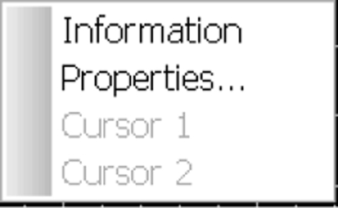
The waveform trace color in Probe can be changed by highlighting the trace and right mouse click > Properties, for release 16.2 (Fig. 3.8) or right mouse click > Trace Property in release 16.3. Both actions will similarly display the Trace Properties box shown in Fig. 3.9.
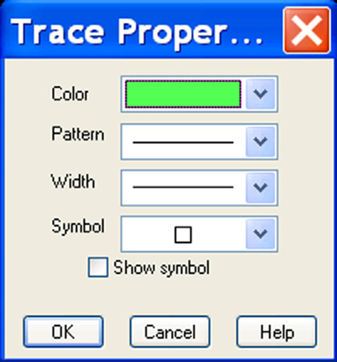
In the Trace Properties box (Fig. 3.9), the trace color, pattern, width, and symbol can be changed.
Note
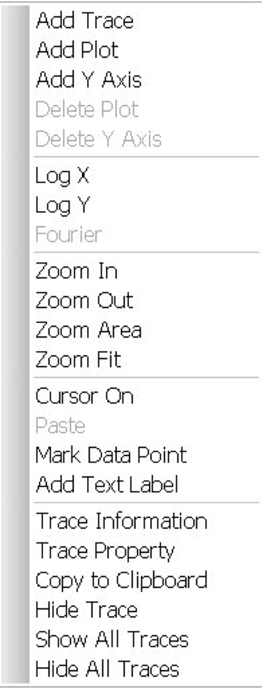
From version 16.3, you can now have the functionality to right mouse button on a trace to open a context-sensitive menu which displays all the related trace options as shown in Fig. 3.10.
From 16.3 you can now change the foreground colors such as the axis and grid lines and also the background color for Probe. Tools > Options > Color Settings as shown in Fig. 3.11.
3.3 Exercises
Exercise 1
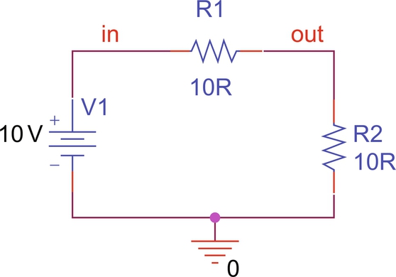
The resistor network circuit in Fig. 3.12 is a potential divider where the ratio of the output voltage to the input voltage is given by
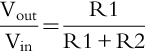
which can be written as:
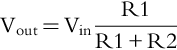
Therefore the output voltage is determined by the ratio of the fixed values of the resistors R1 and R2. If R1 = R2, the output voltage is equal to half of the input voltage.
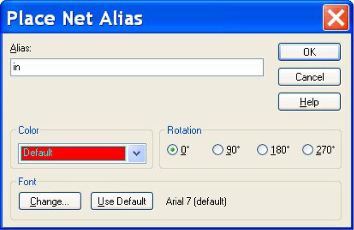
1. Draw the resistor circuit in Fig. 3.12 and name the nodes as shown by selecting Place > Net Alias (Fig. 3.13).
2. Create a PSpice simulation profile, PSpice > New Simulation Profile and for the Analysis type, select DC Sweep. Select the Sweep variable as the voltage source V1 and set up a linear sweep from 0 to 10 V in steps of 1 V, see Fig. 3.14. Click on OK.

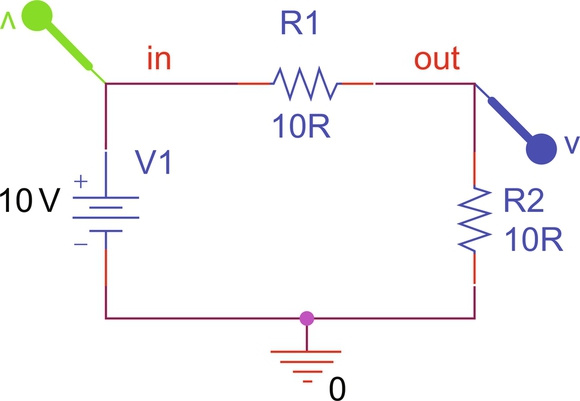
3. Place voltage markers on nodes, in and out (Fig. 3.15).
4. Run the simulation  .
.
5. PSpice will launch and Probe will display the two traces for V(in) and V(out). Fig. 3.16 shows the trace colors are the same as the marker colors in the circuit diagram in Fig. 3.15. Note that the circuit is acting as a potential divider in that the output voltage is half of the input voltage.

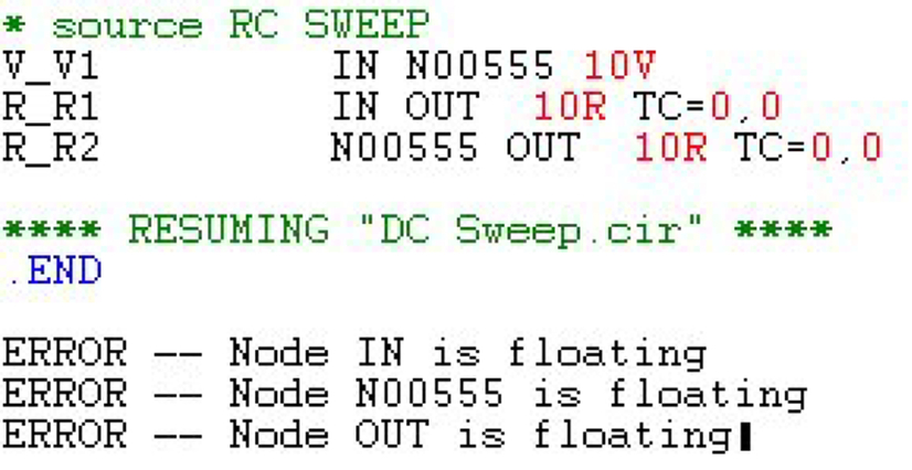
6. Delete the ground symbol and re-simulate. You should see the warning message dialog box (Fig. 3.17) and a message will be displayed asking you to check the Session Log.

7. The Session Log is normally open at the bottom of the screen, if not, the session log can be found from the top tool bar, Window > Session Log. The warning message will read:
WARNING [NET0129] Your design does not contain a Ground (0) net.
8. Click on OK in the Warning message (Fig. 3.15) and PSpice will launch. If the Output file is not displayed, then select, View > Output File. The output file is shown in Fig. 3.18. Your circuit will have different node numbers. The removal of a 0 V symbol was covered in the exercises at the end of Chapter 2 and is mentioned here again as a reminder that in order for the analog voltages to be calculated, a 0 V node must exist in the circuit otherwise nodes will be reported as floating.
9. Re-connect a 0 V symbol. Place > Ground or press G on the keyboard and select a 0 V symbol.
10. Remove resistor R2 from the circuit and simulate.
11. PSpice will start and display the output file with an error message:

12. The Error message relates to no DC path to ground at node out, i.e., the end of the resistor R2 is floating. One other requirement in PSpice is that every node in a circuit must have a DC path to ground. If you need to simulate a node as open circuit, then you can always connect a large value resistor, for example, 100 G ohm or 1T ohm from a node to ground which will provide a DC path to ground without adversely affecting the bias conditions of the circuit.
Similarly, a short circuit can be implemented by a very small resistance of say 1μ ohm or less.
Exercise 2
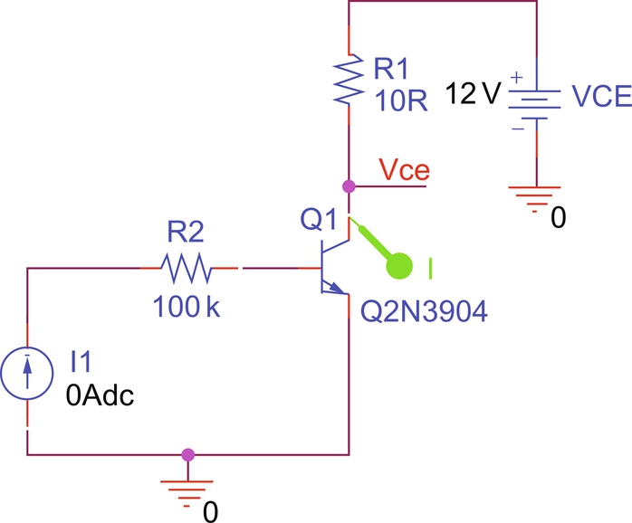
A nested sweep will be performed to display the transistor characteristic family of curves. You will set up the VCE for the transistor as the primary sweep and the base current as the secondary sweep.
In 17.2 you can search for the Q2N3904 transistor using, Place > PSpice Component > Search and entering Q2N3904 in the search field. See Chapter 1, Section 1.3.3, Fig. 1.13. Alternatively follow the following steps.
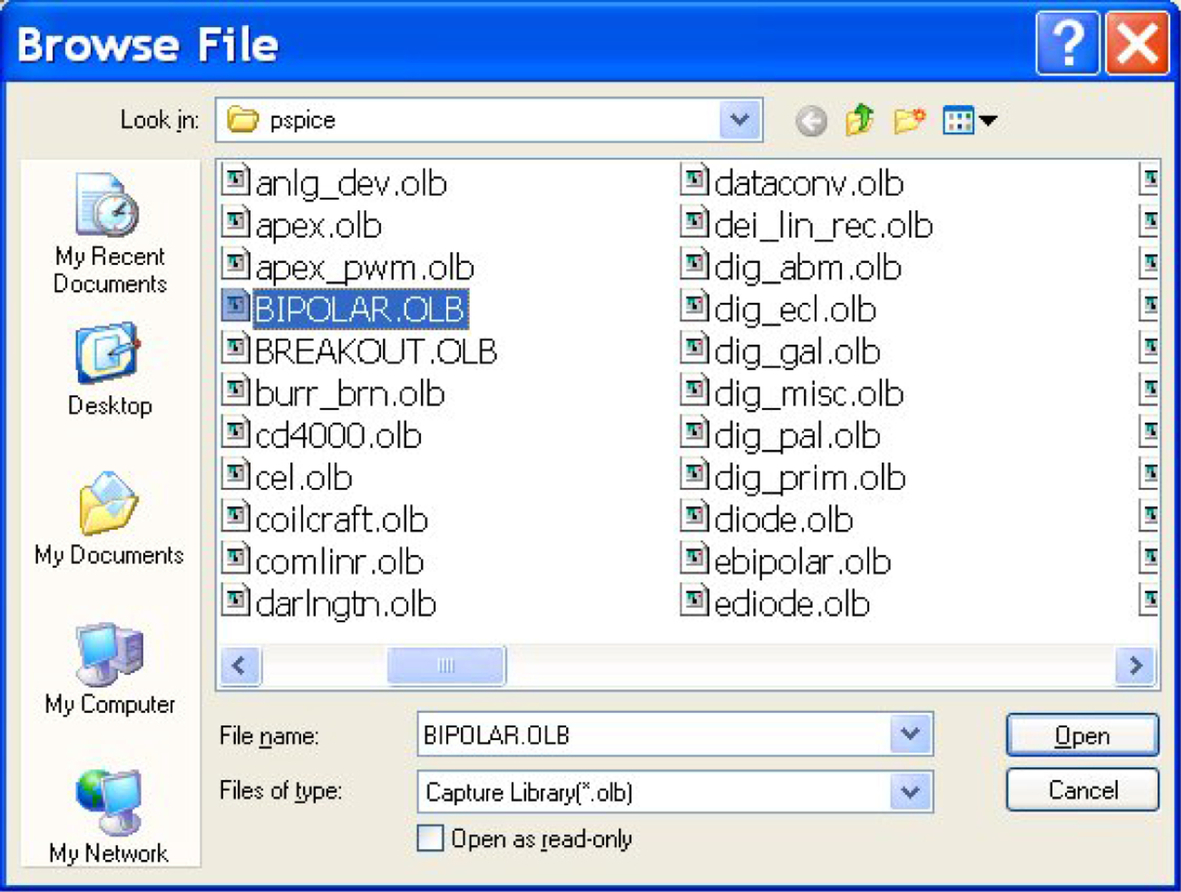
1. Draw the circuit in Fig. 3.19. The transistor can be found in the bipolar library. In the Place Part menu, select the Add Library icon  as shown in Fig. 3.20 or in previous versions, click on Add Library.
This will open up the Browse File window shown in Fig. 3.21. Scroll along or alternatively, type in bipolar.olb in the File name field. Select bipolar.olb and click on Open.

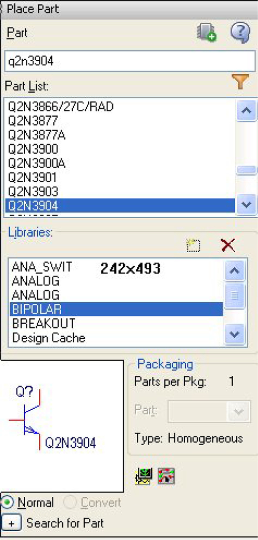
2. The bipolar library will now be added to the list of libraries in the Place Part menu. Select the bipolar library and type in Q2N3904 (not case sensitive) in the Part box, see Fig. 3.22. Double click on the q2n3904 transistor and place in the schematic page.
3. Place the rest of the components as shown in Fig. 3.19. The dc current source, idc is from the source library.
4. You will set up a nested DC Sweep where the VCE will be the primary sweep and the base current the secondary sweep.
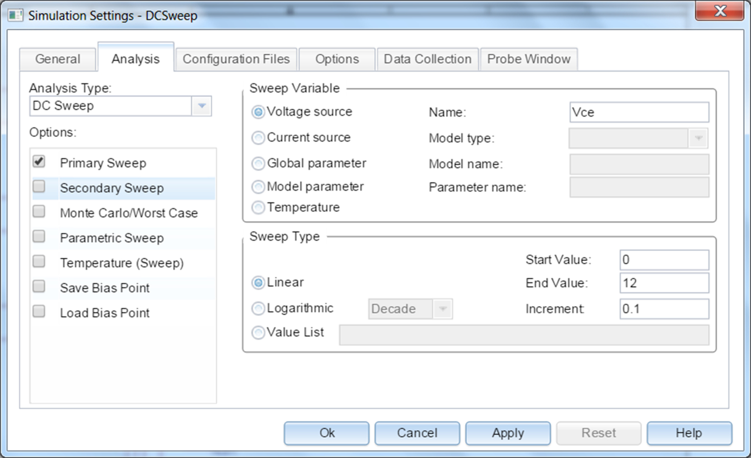
5. Create a simulation profile, PSpice > New Simulation Profile and select the Analysis type to DC Sweep. For the Primary Sweep, which is shown by default, select the Sweep variable to be voltage the source VCE. The Sweep type is Linear with a Start value of 0 V, an End value of 12 V and an Increment of 0.1 V, see Fig. 3.23. Click on Apply but do not exit the Simulation Profile.
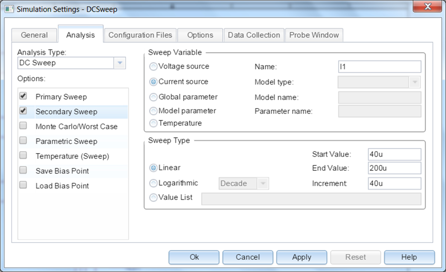
6. In the Options box, select the Secondary Sweep. The Sweep variable is the current source I1. The Sweep type is Linear with a Start value of 40 μA and an End value of 200 μA, the Increment is 40 μA. Make sure the Secondary Sweep box is checked and click on OK, see Fig. 3.24.
7. Place a current marker on the collector pin of the transistor and simulate.
8. You should see the characteristics curves shown in Fig. 3.25.
9. Select Plot > Axis Settings > YAxis and change the Data Range to User Defined and enter a range from 0 mA to 40 mA. Click on OK and see the change.
10. Select Plot > Axis Settings > YGrid and uncheck Automatic and set the Major Spacing to 10 m. Click on OK and see the change.
11. Select Plot > Axis Settings > XGrid and uncheck both Major and Minor Grids to None. Click on OK and see the change.
12. Select Plot > Axis Settings > YGrid and uncheck both Major and Minor Grids to None. Click on OK and see the change.
13. Select Plot > Label > Text, change the font color to silver and add the base currents as shown in Fig. 3.26.