Worst Case Analysis
Abstract
Worst Case analysis is used to identify the most critical components which will affect circuit performance. Initially a sensitivity analysis is run on each individual component which has a tolerance assigned. The component value is effectively pushed toward both of its tolerance limits by a small percentage of its value to see which limit would have the most effect on the worst case output. A Worst Case analysis is then performed by setting all the component values to their end tolerance limits which gave an indication of the worst case results. In order to reduce the number of simulation runs, collating functions can be used to detect differences from the nominal worst case output such as minimum, maximum, or threshold differences.
Keywords
Circuit; Analog design; Collating functions; Frequency; Sensitivity; Simulation
Worst Case analysis is used to identify the most critical components which will affect circuit performance. Initially a sensitivity analysis is run on each individual component which has a tolerance assigned. The component value is effectively pushed toward both of its tolerance limits by a small percentage of its value to see which limit would have the most effect on the worst case output. A Worst Case analysis is then performed by setting all the component values to their end tolerance limits which gave an indication of the worst case results. In order to reduce the number of simulation runs, collating functions can be used to detect differences from the nominal worst case output such as minimum, maximum, or threshold differences.
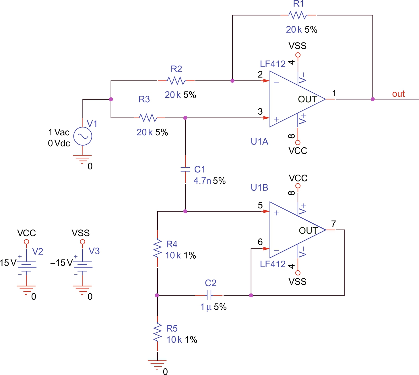
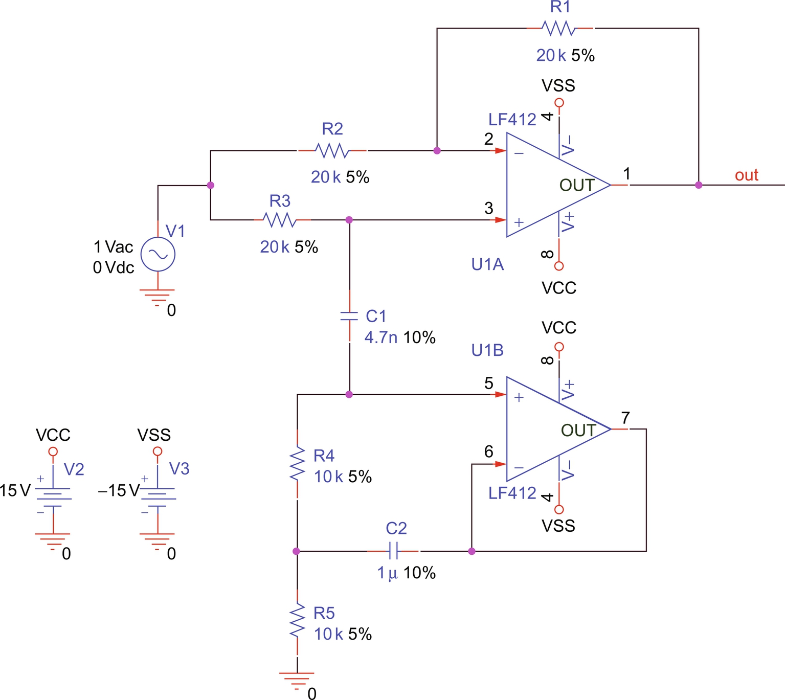
In Fig. 11.1, an equivalent inductor circuit known as a gyrator is implemented using U1B, R4, R5, and C2 which enables a high inductance value to be realized, 100H in this example. The series connection of the equivalent inductor and C1 forms a series tuned circuit which determines the frequency of the notch filter. Using ideal component values, the initial simulation results will show the required notch filter response. However, components have tolerances which may affect the notch frequency. Adding component tolerances, a Worst Case analysis will determine which components are critical to the circuit's performance. The notch frequency can be determined by detecting the minimum output voltage of the filter. Therefore a Worst Case analysis can be run using a Collating function on the output voltage which will only record the minimum output voltages.
11.1 Sensitivity Analysis
What we are looking to investigate is the effect each component has on the notch frequency by recording the minimum output voltage of the filter and hence determine which components are critical to the notch frequency. A sensitivity analysis will be run on each component in turn with its sensitivity value given by
value = nominal value ⁎ (1 + RELTOL)
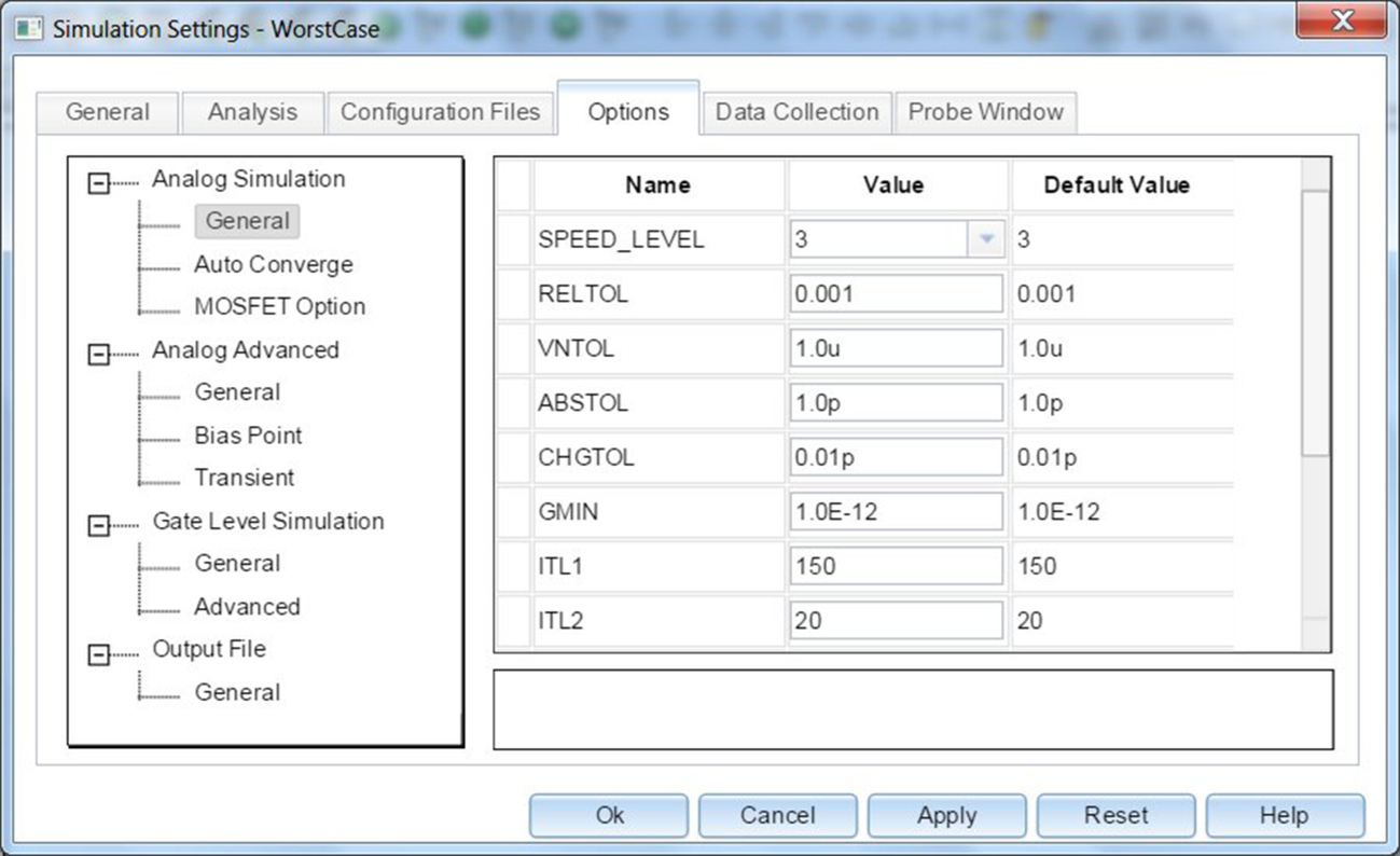
where RELTOL is the relative tolerance and can be found in the PSpice Simulation Settings > Options as shown in Fig. 11.2. By default, RELTOL is 0.001 (0.1%).
For example, R1 has a value of 20 kΩ and a tolerance of 5% and so has an expected value between 19 kΩ and 21 kΩ. If RELTOL is set to 0.01 (± 1%), the resistor value will be increased to 20200 Ω and then decreased to 19800 Ω. The direction in which the change in resistor value, gave the worst case result (minimum voltage), determines which tolerance limit (upper or lower) to use in the Worst Case analysis. If the minimum output voltage was recorded with a 1% decrease in the resistor value, then the lower tolerance limit of 19 kΩ will used for R1 in the Worst Case analysis.
The value of R1 is then reset to its nominal of 20 kΩ value and a sensitivity analysis is performed on R2, varying its value toward its tolerance limits and recording the “tolerance direction” which gave the minimum gain. The resistor values will then be set to their tolerance limit value which gave the worst case minimum gain and the gain of the amplifier will be calculated.
It must be remembered that the above assumes that the output voltage decreases continuously with a decrease in R1 and that there is no interdependencies on other components which may not be the case.
11.2 Worst Case Analysis
Based upon the results of the sensitivity analysis, Worst Case analysis sets the component values to one of their tolerance limits. If R1, 20 kΩ − 1% gave the minimum voltage, then R2 will be set to 20 kΩ − 5%.
A Worst Case analysis is run in conjunction with a DC, AC, or transient analysis and does not take into account the interdependence of the parameters. The results of the sensitivity and Worst Case analysis are written to the output file.
11.3 Adding Tolerances
As with Monte Carlo analysis, tolerances can be added directly to the R, L, and C Capture parts in the schematic. Alternatively, breakout parts can be used and the following dev or lot statements are added as used with a Monte Carlo analysis.
.model Rwc1 RES R = 1 dev = 5% lot = 2%
The dev statement causes the tolerance values of devices that share the same model name to vary independently from each other, while the lot statement will cause the tolerance values of devices to track together.
As with a Monte Carlo analysis, you have to define an output variable which can be a node voltage or an independent current or voltage source. In Fig. 11.3, the output variable is V(out).

11.4 Collating Functions
As with Monte Carlo, collating functions detect and compare the output response of the circuit with defined parameters. There are five functions which define the worst case results.
YMAX finds the greatest distance in the Y direction in each waveform from the nominal run.
MAX finds the maximum value of each waveform.
MIN finds the minimum value of each waveform.
RISE_EDGE(value) finds the first occurrence of the waveform crossing above the threshold (value). The function assumes that there will be at least one point that lies below the specified value followed by at least one above.
FALL_EDGE(value) finds the first occurrence of the waveform crossing below the threshold (value). The function assumes that there will be at least one point that lies above the specified value followed by at least one below.
11.5 Exercise
1. Draw the circuit in Fig. 11.4. The LF412 dual opamp is from the source library or you can use any opamps.
2. Select all the resistors by using holding down the control key and right mouse button > Edit Properties.
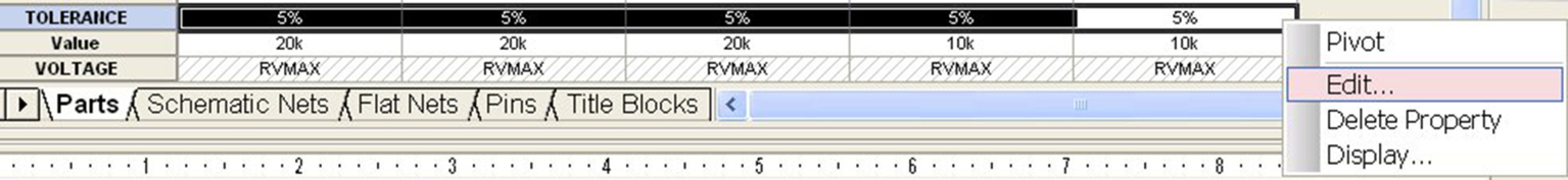
3. In the Property Editor, select and highlight the whole row (or column) for the Tolerance property and rmb > Edit, see Fig. 11.5.
Add a 5% tolerance in the Edit Property Values window as shown in Fig. 11.6 and click on OK and then close the Property Editor.

4. Repeat steps 3 and 4 adding a 10% tolerance to the capacitors, C1 and C2.
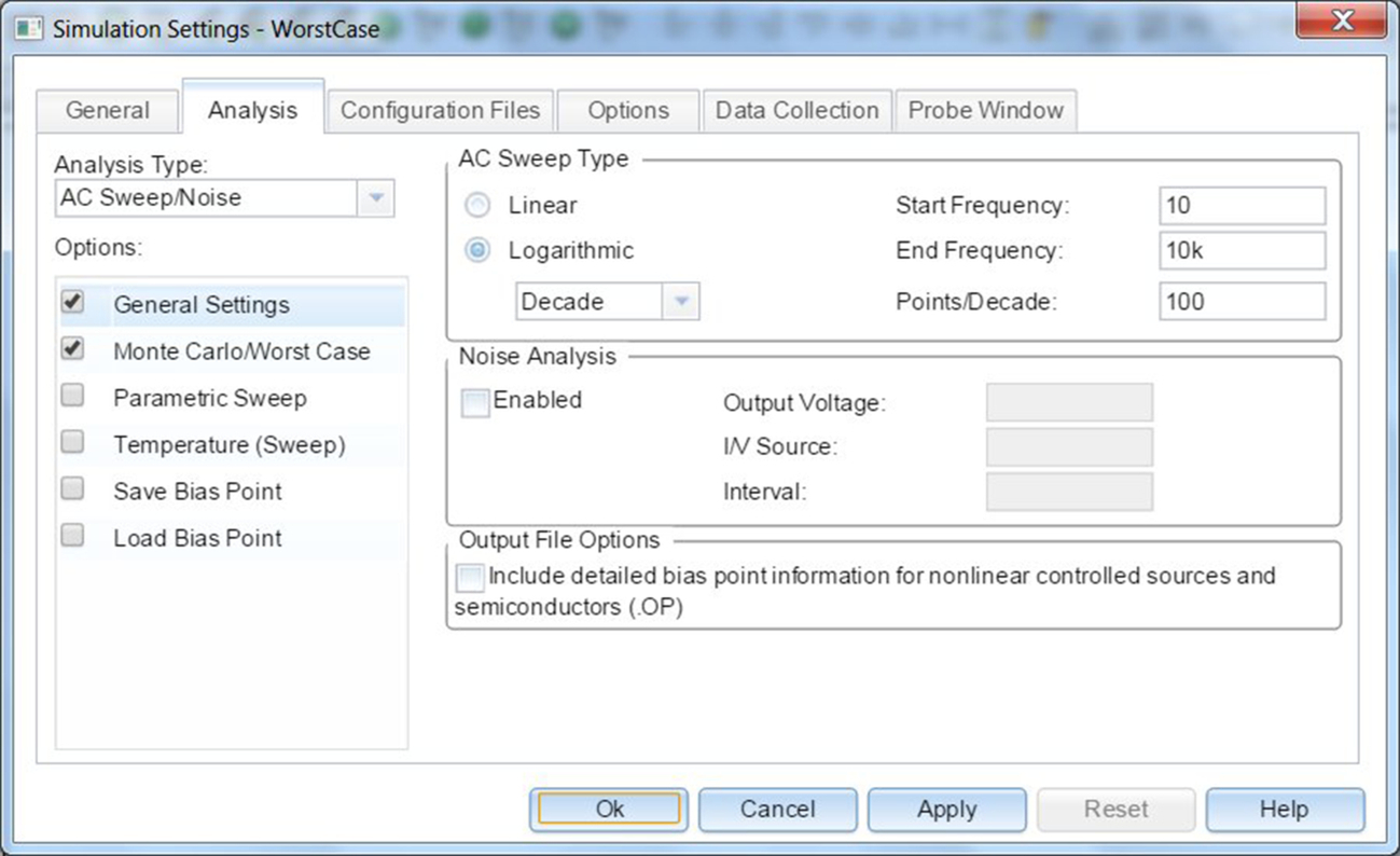
5. Set up a simulation profile for an AC Sweep from 1 Hz to 10 kHz performing a logarithmic sweep with 100 points per decade, see Fig. 11.7. Click on Apply but do not exit.
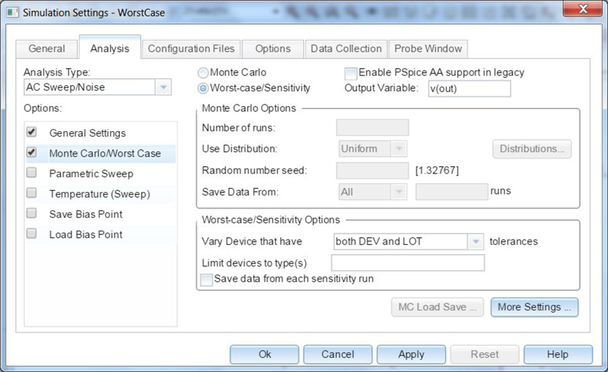
6. In the simulation profile, in Options select Monte Carlo/Worst Case and enter V(out) for the Output variable, see Fig. 11.8. Click on Apply but do not exit.
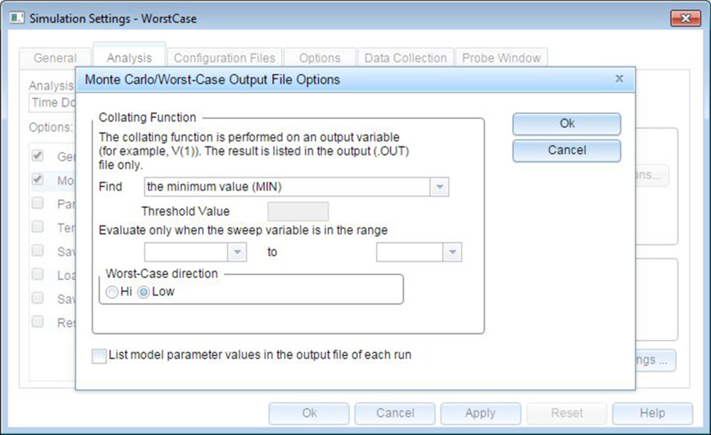
7. Click on More Settings and in Find, select the minimum (MIN) for the Collating Function and select Low for the Worst Case Direction as shown in Fig. 11.9. Click on OK but do not exit.
The Options window is different between pre and post 17.2 software versions. If you have pre 17.2 then follow steps 8.1 and 8.2. If you have post 17.2, then follow steps 9.1 and 9.2 to set the options.
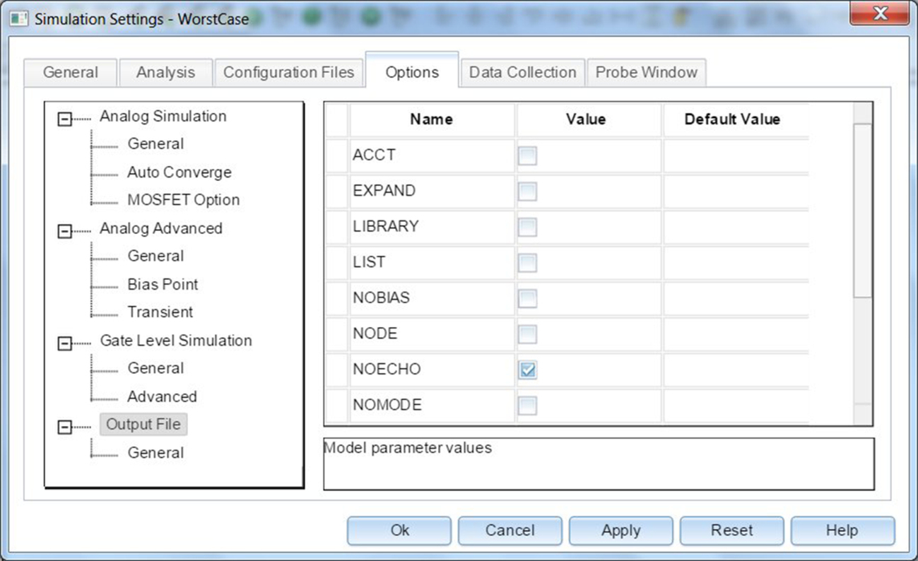
8.1. Select the Options tab and select Output File and uncheck, Bias Point Node Voltages and Model parameter values as shown in Fig. 11.10. Click on OK but do not close the simulation profile window.
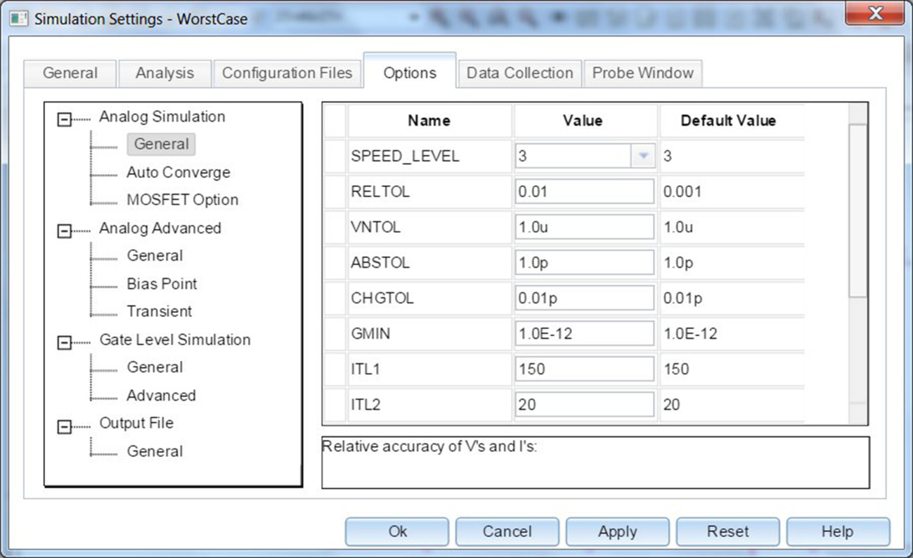
8.2. In the simulation profile, select Options and change RELTOL to 0.01, see Fig. 11.11. Click on OK to close the simulation settings profile.
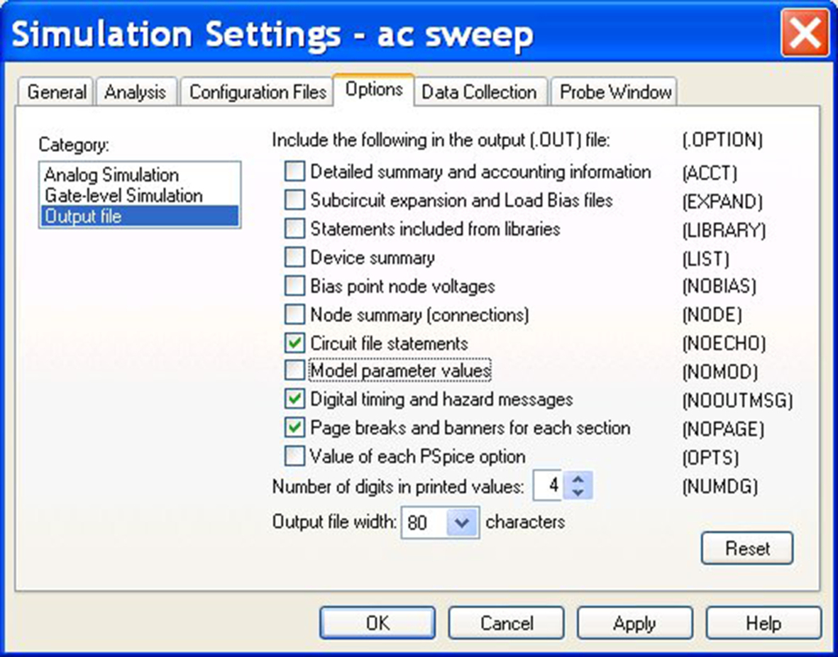
9.1. Select the Options tab and select Output File and uncheck, Bias Point Node Voltages and Model parameter values as shown in Fig. 11.12. Click on Apply but do not close the simulation profile window.
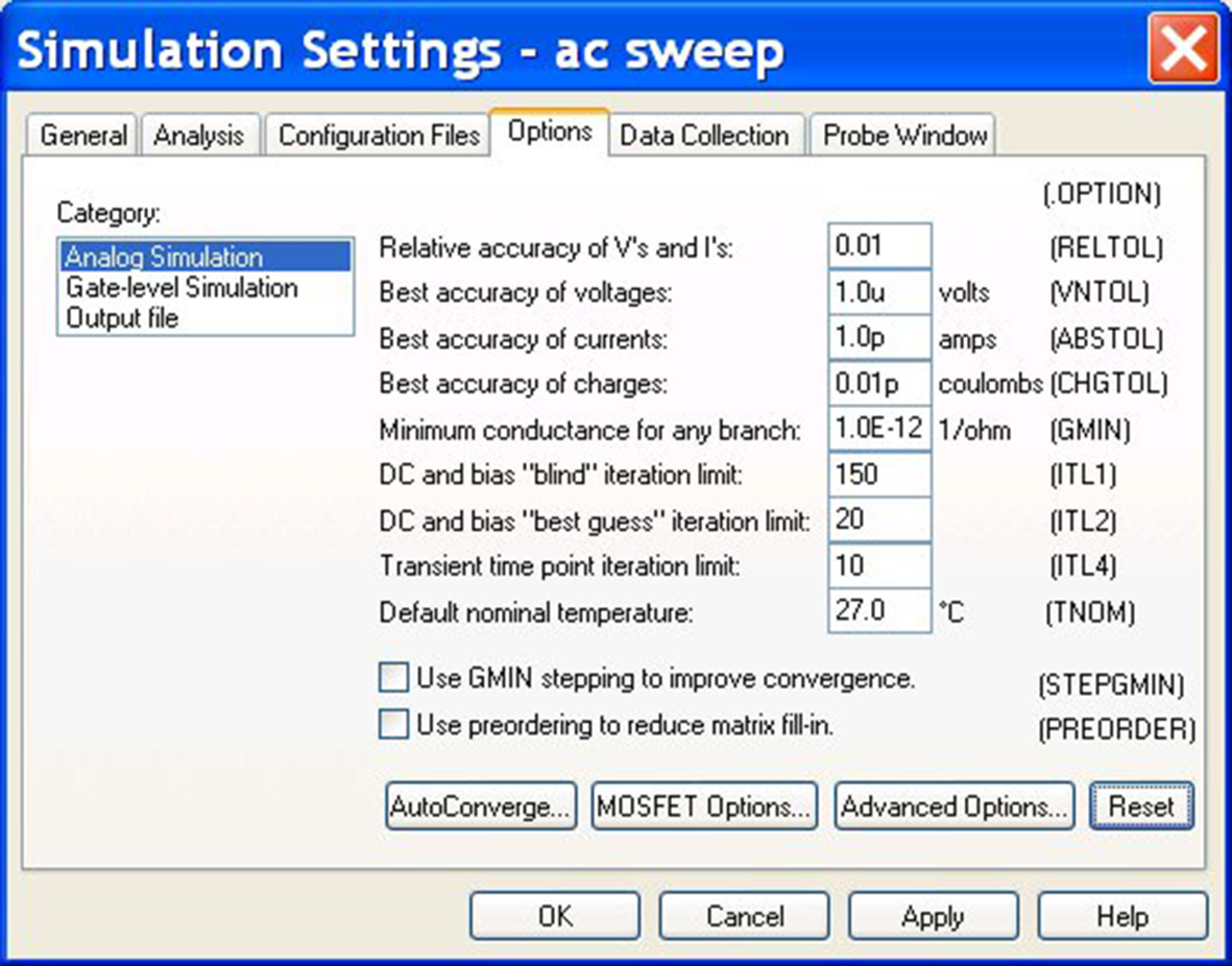
9.2. In the simulation profile select Options > Analog Simulation > General and change RELTOL to 0.01, see Fig. 11.13. Click on OK to close the simulation settings profile.
10. Place a Vdb marker on node out, (PSpice > Markers > Advanced > dB Magnitude of Voltage).
11. Run the simulation. 
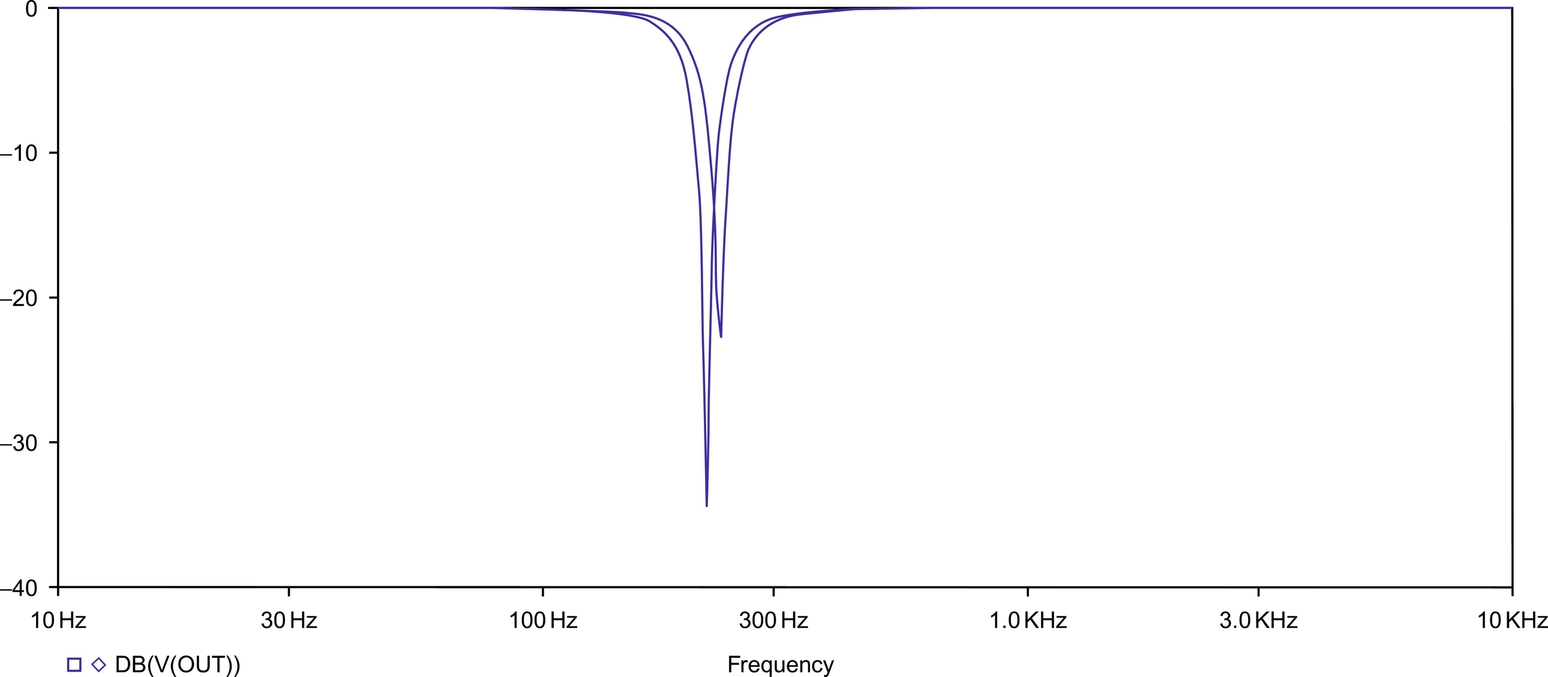
12. In Probe you will see two output notch responses. The nominal response is at 234 Hz and the Worst Case response is at 199 Hz, see Fig. 11.14.

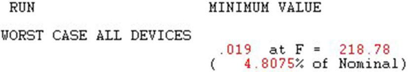
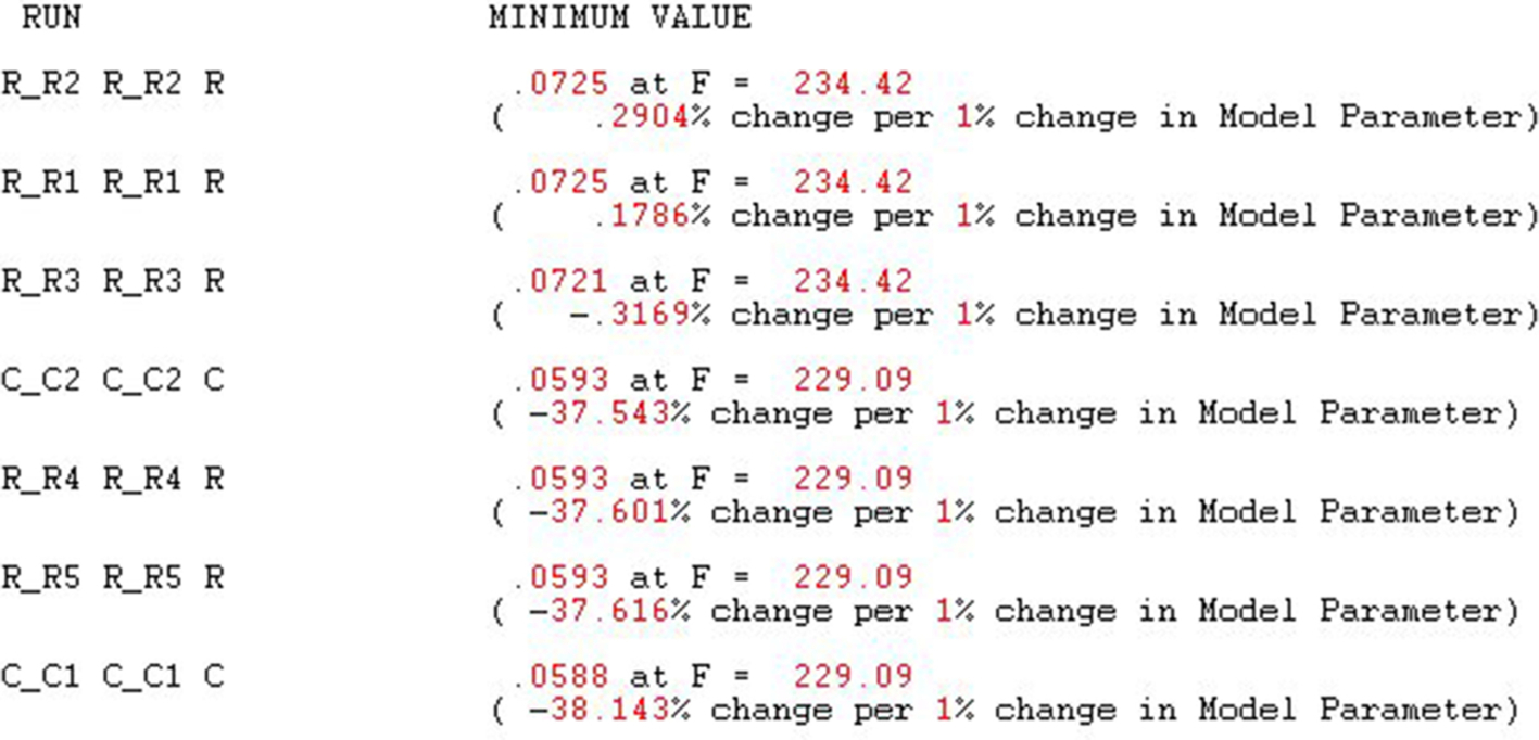
13. Open the Output File and scroll down to the list of Minimum values as shown in Fig. 11.15. Here as expected R4, R5, C1, and C2 have a greater effect on the notch output voltage compared to R1, R2, and R3.
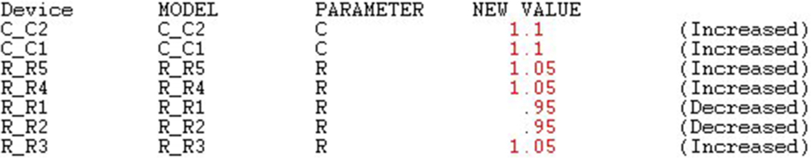
Scroll down to Worst Case All Devices as shown in Fig. 11.16 where you can see as the result of the sensitivity analysis, the tolerance direction in which the component values were set for the Worst Case analysis.
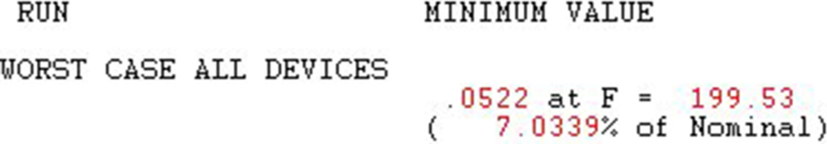
14. At the bottom of the Output File is the Worst Case summary showing that the worst case scenario is for the notch filter frequency at 199 Hz which is a deviation of 7% from the nominal (Fig. 11.17).
15. Change the tolerance of the capacitors to 5% and resistors R4 and R5 to 1% and run the simulation to see if this improves the predicted Worst Case response.
16. Fig. 11.18 shows an improvement in the Worst Case notch frequency that is given in the summary as 218 Hz (Fig. 11.19) being closer to the nominal frequency of 234 Hz.