
DC Bias Point Analysis
Abstract
When you connect a battery or a power supply to a circuit, the circuit voltages and currents effectively settle down to what is known as a DC steady-state condition. This is also known as the operating point or Bias Point of a circuit under steady-state conditions. In PSpice, the Bias Point analysis calculates the node voltages and currents through the devices in the circuit. For example, for a simple common emitter transistor amplifier, the Bias Point analysis will calculate the base, emitter, and collector bias voltages and the base, collector, and emitter quiescent currents.
Keywords
Bias; Circuit; Simulation; Emitter; Voltage; Output file
When you connect a battery or a power supply to a circuit, the circuit voltages and currents effectively settle down to what is known as a DC steady-state condition. This is also known as the operating point or Bias Point of a circuit under steady-state conditions. In PSpice, the Bias Point analysis calculates the node voltages and currents through the devices in the circuit. For example, for a simple common emitter transistor amplifier, the Bias Point analysis will calculate the base, emitter, and collector bias voltages and the base, collector, and emitter quiescent currents.
Bias Point analysis will also take into account any voltage sources applied to the circuit and any initial conditions set on devices or nodes in the circuit. For example, you may want to preset a capacitor to a known voltage or set an initial digital state, a logic “1” or “0” on a digital device.
The calculated Bias Point voltages and currents are also used as a “starting point” for the other circuit analysis calculations. For example, when you run a transient (time) or an AC (frequency) analysis, PSpice automatically runs a Bias Point analysis first. However, the Bias Point analysis can be turned off for special cases in which a DC steady-state solution cannot be found. This is especially useful in the case of an oscillator which relies on the fact that it has no steady-state condition.
With the Bias point enabled, the output file will provide a list of all the analog and digital node voltages, the currents and total power of all voltage sources in the circuit, and a list of small signal parameters for all devices in the circuit. There is an option to suppress the bias information in the PSpice simulation profile.
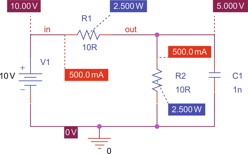
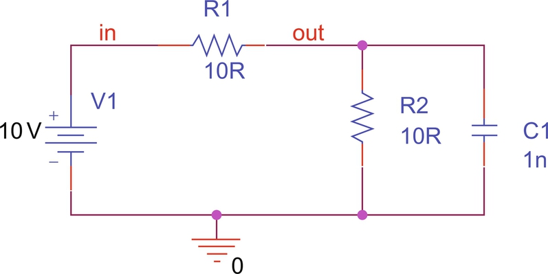
The RC circuit in Fig. 2.1 is based upon the resistor circuit in Chapter 1. A capacitor, C1 has been added in parallel with R2. With the circuit drawn, a PSpice simulation profile needs to be set up. The settings are accessed from the top tool bar, PSpice > New Simulation Profile. This is where the different analysis types for DC, AC, transient, and Bias Point are selected. By default, Bias Point is selected.
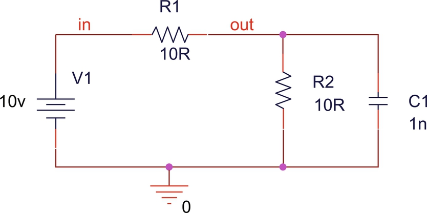
Fig. 2.2 shows the default PSpice Simulation Profile for a DC Bias Point Analysis. For this example, the default settings are used.

Note
The latest 17.2 version of the Simulation Settings window shown in Fig. 2.2 for Bias settings now has an HTML look to it but has the same functionality.
To run the simulation, you select PSpice > Run or you can select the play button.
Note
When you run a simulation, the PSpice Netlist Generation dialog box shown in Fig. 2.3 appears.

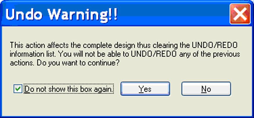
In previous versions when you first run a simulation, the Undo Warning dialog box shown in Fig. 2.4 will appear. This just states that you will not be able to undo or redo any previous actions. Just check the Do not show this box again as shown in Fig. 2.4 and click on Yes.
In 17.2 the appearance of the PSpice Simulation Profile Settings has changed to an HTML look.
2.1 Netlist Generation
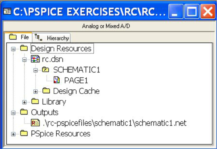
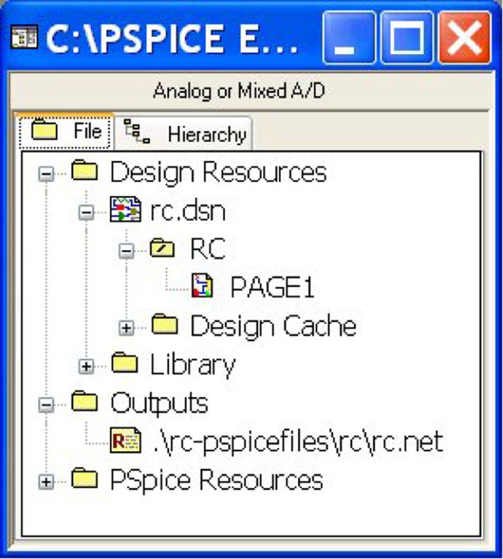
The circuit diagram drawn in Capture is represented as a netlist of all the components and their respective connections to other components. This netlist is automatically generated when you run the simulation and can be seen in the Outputs folder in the Project Manager, see Fig. 2.5.
Note
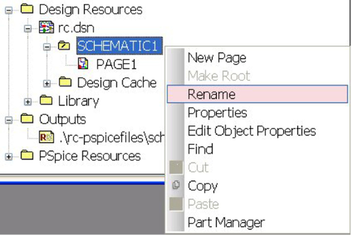
By default the circuit diagram is called SCHEMATIC1 and so the generated netlist is called schematic1.net as seen in Fig. 2.5. To rename the schematic, select the SCHEMATIC1 name, right mouse click, and select Rename as shown in Fig. 2.6, entering RC as the new schematic name.
When you run the simulation an rc.net netlist will appear in the outputs folder. Fig. 2.7 shows the original schematic1.net and the newly generated rc.net. Note that Capture is not case sensitive. Any schematics named in upper case will generate lower case named netlist files (Fig. 2.7).

To open the netlist file, double click on the name and the netlist will appear as shown in Fig. 2.8.

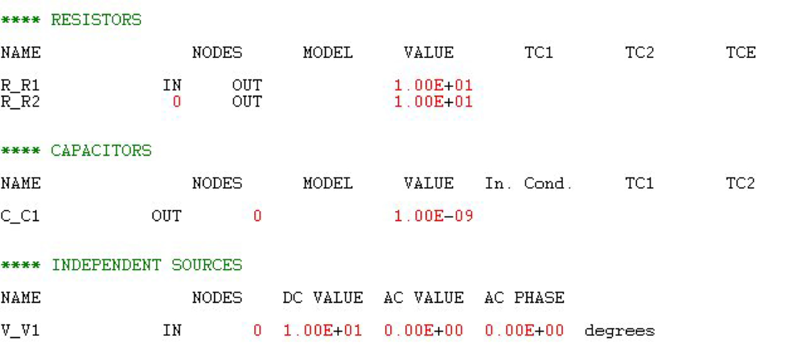
The netlist in Fig. 2.8 shows that resistor R1 is connected between nodes, IN and OUT, has a value of 10 ohms, and a zero temperature coefficient (TC). The voltage source, V1, is connected between IN and 0 V and has a value of 10 V. The R_ indicates that this is a flat netlist compared to a hierarchical netlist. Resistor properties and hierarchical circuits will be discussed in more detail in a later chapter. For now, the netlist defines the net connections between R1, R2, and V1 and any defined net names.
When you run a PSpice simulation, PSpice is launched and the PSpice environment window appears. However, there is no graphical output for a DC Bias Point analysis as no waveform data is calculated and hence no traces are available to be plotted. Instead you can look in the Output File to see the calculation results or view on the schematic, the bias voltages, currents, and instantaneous power for the circuit components. From the top toolbar in Capture or PSpice, select View > Output File and scroll to the bottom of the file (see Fig. 2.9). Because the nets have been named, you can easily see the calculated output voltages and currents. Remember, during a DC Bias Point analysis, capacitors are open circuit, hence the RC circuit is behaving as a simple potential divider with R1 and R2 dividing the 10 V DC voltage down to 5 V on the “out” net.
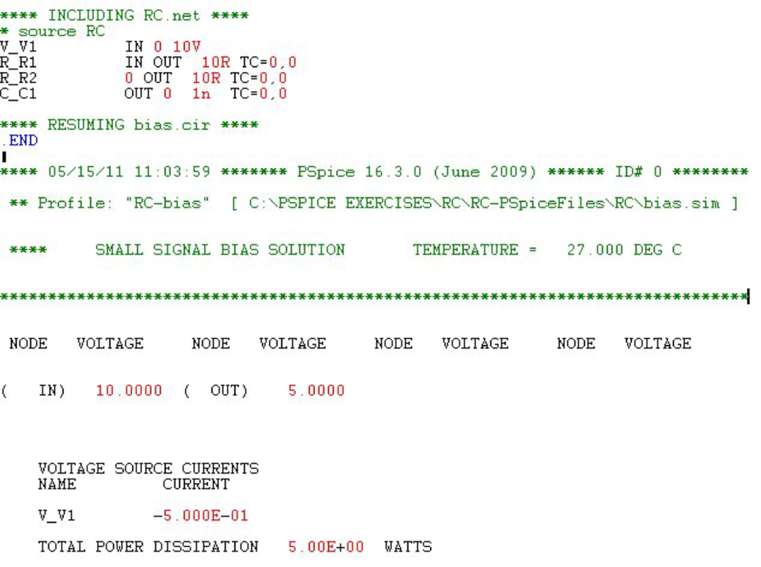
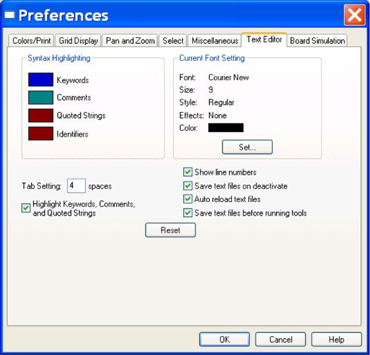
A new feature (in release 16.3) as seen in Fig. 2.9 is the use of colors in the output file to highlight the different syntax such as text, component values, comments, expressions, and keywords. The default colors can be changed by selecting, Options > Preferences > Text Editor as shown in Fig. 2.10.
The Output File also highlights any errors and warnings that may have occurred and is useful to determine where the errors occur. See the exercises at the end of the chapter for an example.
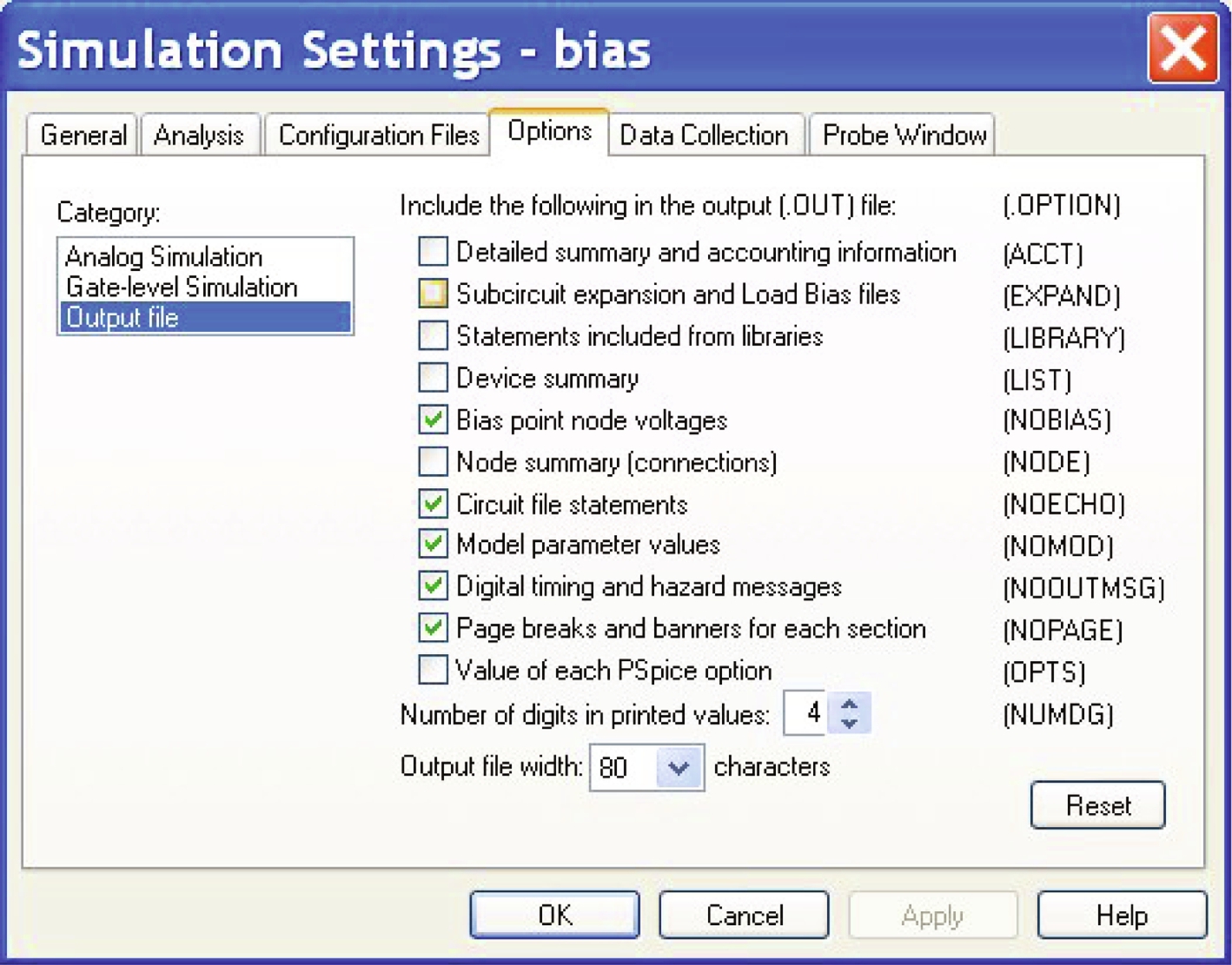
As mentioned previously, the output file provides a report on the analog and digital node voltages and device currents together with a list of small signal parameters for the devices in the circuit. There is the option to suppress the bias information reported in the output file. Under the Options tab in the PSpice Simulation profile (Simulation Settings), select Output file in the Category: box as shown in Fig. 2.11 and uncheck the (NOBIAS) option. There is also the option to list all the devices (LIST) in the circuit, summarizing their connecting nodes, values, models, and other parameters. Fig. 2.11 shows the other available options available for the output file. The Reset button resets all the options back to their default settings.
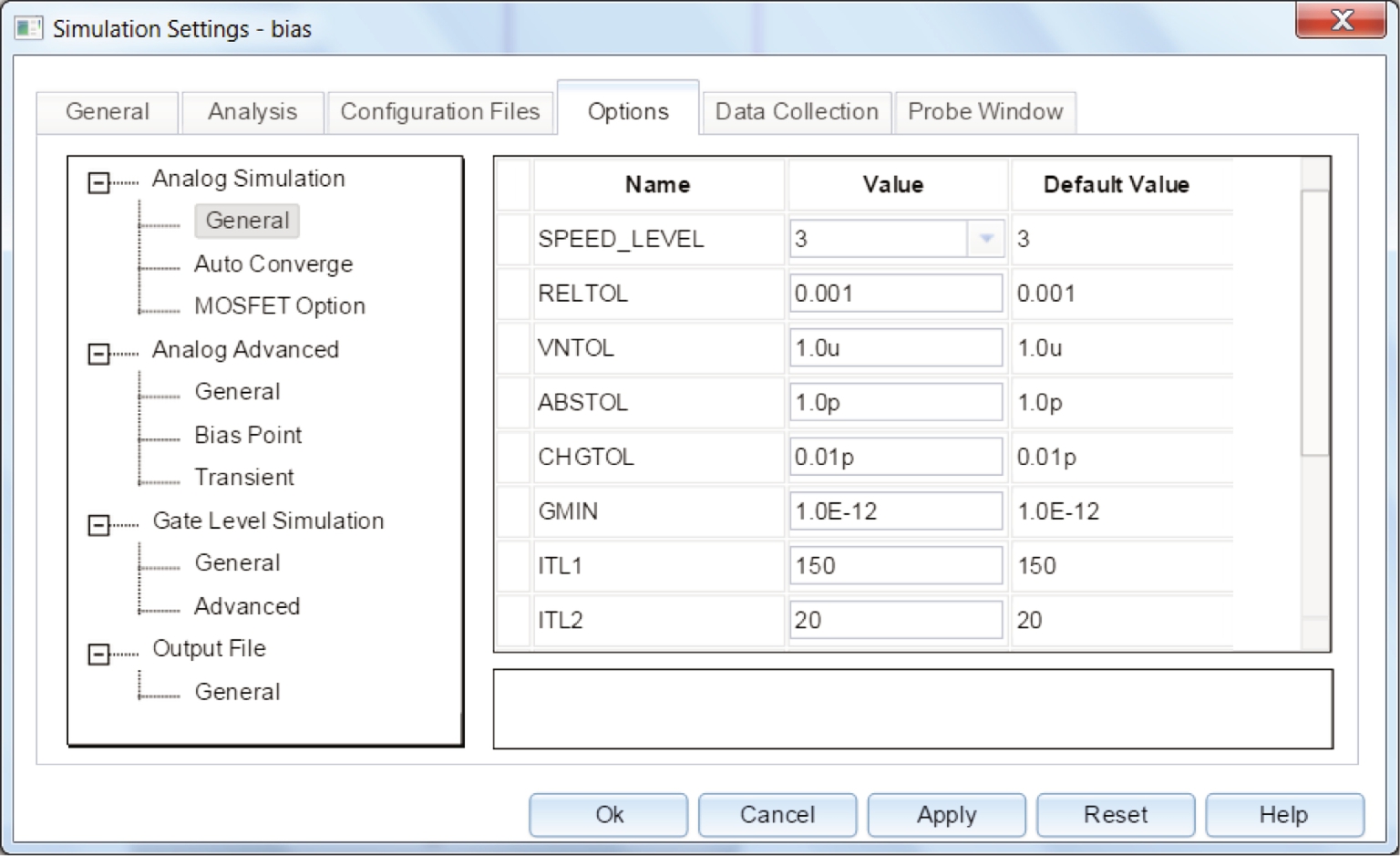
Fig. 2.12 shows the PSpice Simulation Settings window with previous software versions. The new 17.2 layout makes it easier to navigate and access all available options.
2.2 Displaying Bias Points
After a simulation is run, the bias voltage, current, and power values can be displayed on the schematic. In Capture, select PSpice > Bias Points > Enable or select the bias display icons which have changed in appearance in release 16.3. See Figs. 2.13 and 2.14.
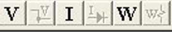

Fig. 2.15 shows the displayed bias voltages, currents, and instantaneous power for the resistor RC circuit.
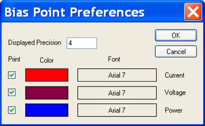
The number of significant digits displayed for bias points can be changed by selecting, PSpice > Bias Points > Preferences as shown in Fig. 2.16. Up to 10 Precision digits can now be displayed.
Individual bias values can be turned on and off for voltage, current, or power. For example, if you select a wire net, the voltage icon will be activated  which will enable you to toggle the value for bias voltage on or off for a selected wire.
If you select a component pin, the current icon will be activated  which will enable you to toggle the value for bias current on or off for a selected part.
If you select a component, the instantaneous icon will be activated  which will enable you to toggle the value for bias power on or off for a selected part.
2.3 Save Bias Point
You can save and reuse the Bias Point data from a simulation which is useful if you have to run a number of simulations on a large circuit which has a long simulation run time. This is assuming that the circuit netlist, i.e., the connectivity of the components has not changed. Remember that other analyses use the calculated results from a Bias Point analysis so when you resimulate the circuit, assuming that the netlist has not changed, the initial Bias Point calculations can be saved and reused thus reducing the simulation run time. Saving the Bias Point is also useful when a simulation fails to converge to a solution.
In the Simulation Profile Settings, select Bias Point analysis and then select Save Bias Point. As you can see in Fig. 2.17, the data from the Bias Point analysis is saved in a file called saved_bias_point.txt. You select the Browse… button to select or create the folder in which to save the file.
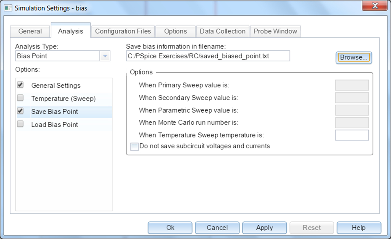
The Bias Point saved data contains node voltages and digital states for all the devices in the circuit, the total power and current supplied by any voltage sources, and a list of model parameters for the devices in the circuit.
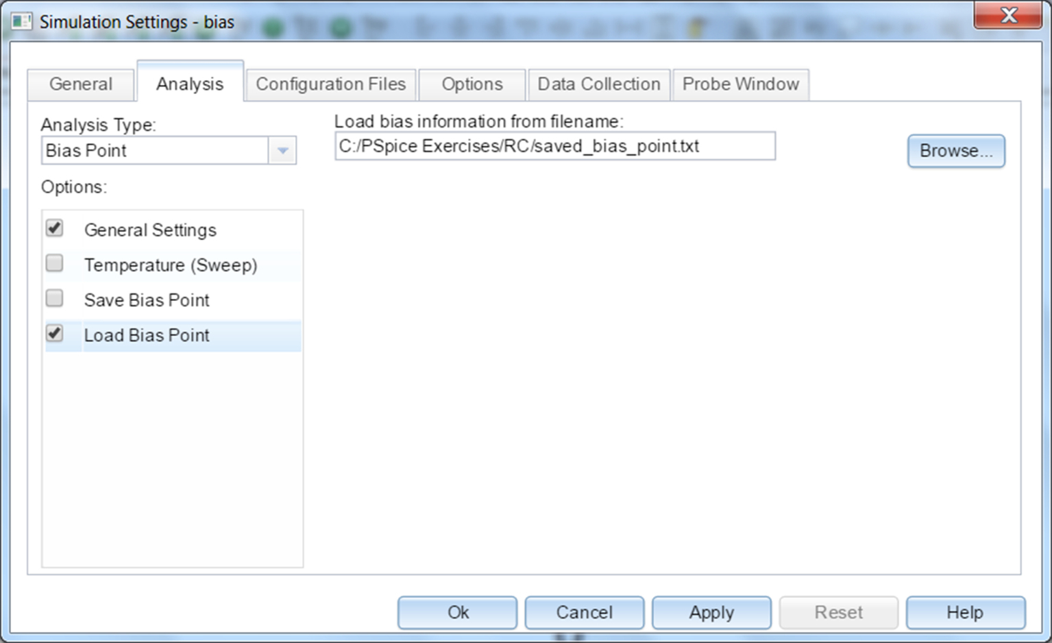
2.4 Load Bias Point
Saved Bias Point analysis data is loaded by selecting the Load Bias Point option in the simulation profile. Fig. 2.18 shows a previously saved Bias Point data file being selected. Bias Point information can also be saved and used for a DC Sweep and a Transient analysis.
2.5 Exercises
Exercise 1
1. The circuit in Fig. 2.19 is based upon the resistor circuit in Chapter 1. Add a 1n capacitor, from the analog library, in parallel with R2.
2. Delete the 0 V volt symbol and resimulate. A warning message will appear (Fig. 2.20) asking you to check the Session Log which is normally open at the bottom of the screen in Capture.
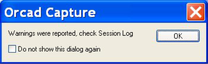
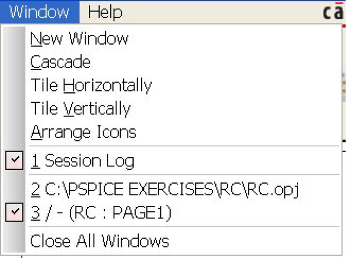
You may have to expand the window upwards to see the complete message. If the session log is not visible, it can be found from the top tool bar, Window > Session and should contain the following message.
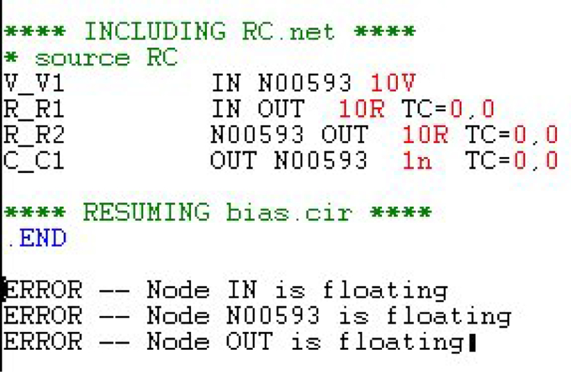
WARNING [NET0129] Your design does not contain a Ground (0) net.
Your reported net number shown will be different to the earlier one. The PSpice window will then open and display the output file which will report that a number of numbered nodes are floating (see Fig. 2.21).
3. In the RC circuit, reconnect the ground symbol and resimulate. There should be no errors.
In the capsym library there are other ground symbols as shown in Fig. 2.22. For PSpice simulations, make sure that you select the ground symbol with the 0 showing. The other symbols can be placed in the circuit to show the difference between ground connections as long as there is a 0 V node in the circuit.

4. Create a bias point simulation profile based upon the initial bias point.
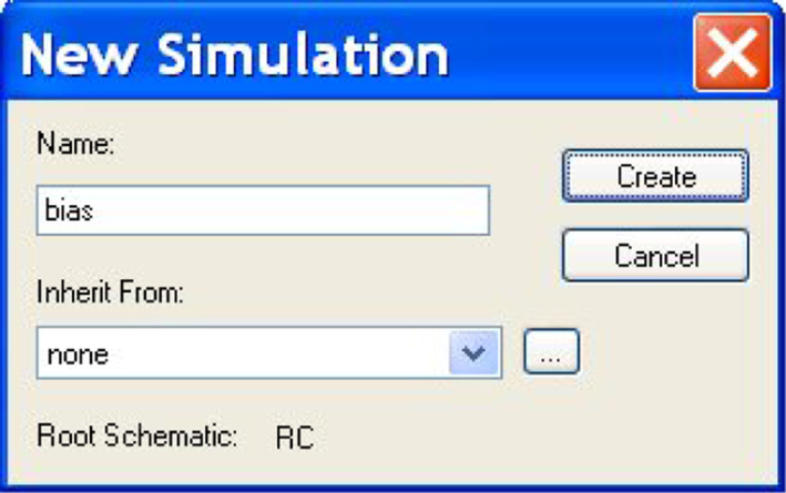
PSpice > New Simulation Profile or click on the icon  and enter bias for the simulation Name, see Fig. 2.23 and click on Create.
5. The dialog box in Fig. 2.24 will appear telling you that a simulation profile of the same name already exists. New projects include a default Bias Point simulation profile called Bias.
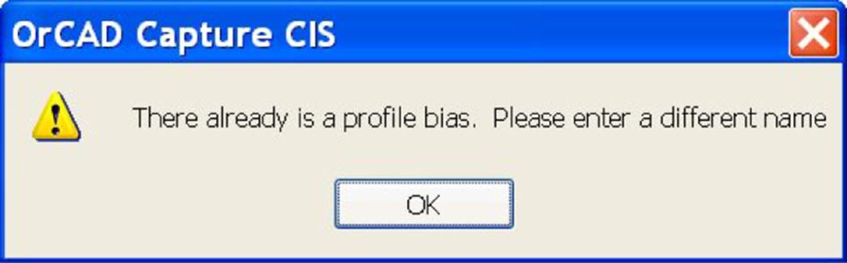
Click on OK and Capture will automatically present you with a new name of bias1 (Fig. 2.25). Click on Create.

6. The simulation settings window will appear. Fig. 2.26 shows the 17.2 version of the simulation settings that has the same functionality. If not already set by default, select the Analysis type to Bias Point. Click on Apply but do not exit.

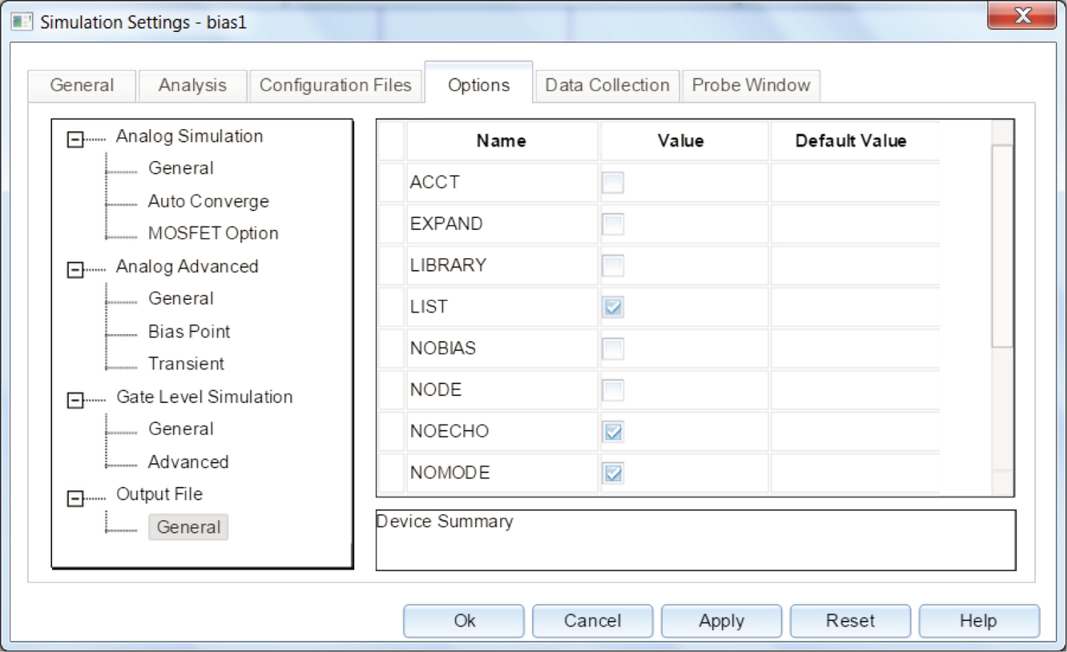
7. If you are using 17.2 or later, select the Options tab and then select Output File > General. Uncheck NOBIAS and check LIST as shown in Fig. 2.27.
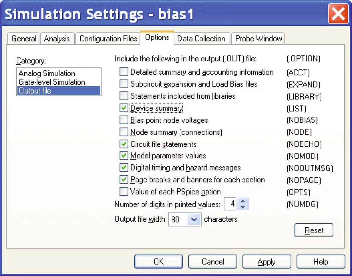
If you are using previous versions to 17.2; under the Options tab, select Output File in the Category: box and uncheck (NOBIAS) and check (LIST), see Fig. 2.28. Click on OK.
8. Run the simulation. When PSpice launches, select View > Output file. The output file shows a summary of the resistors, capacitor, and voltage source used in the circuit as shown in Fig. 2.29. The output voltages and currents are not reported in the output file.
9. Create another new PSpice simulation profile but this time the bias point simulation settings will be inherited from the previous bias1 point simulation profile. In the New Simulation window, enter bias2 for the Name. Click on the pull down Inherit From menu as shown in Fig. 2.30, select bias1 and click on Create. In the simulation settings, you will see the Bias Point analysis is selected. Select Options > Output file and you will see LIST is checked and NOBIAS is unchecked. Close on OK to close the new simulation profile.

You now have created three bias point simulation profiles, bias, bias1, and bias2.
10. If not already displayed, open the Project Manager window by either selecting, Window > < project path >RC.opj file (Fig. 2.31) or click on the icon 
 .
.
The Project Manager will be displayed as shown in Fig. 2.32.
11. In the Project Manager window, expand the PSpice Resources > Simulation Profiles. The three bias point analysis simulation profiles that have been created are listed in the Project Manager (Fig. 2.33) and are also displayed on the left-hand side of the top tool bar (Fig. 2.34) in which a pull down menu lists the simulation profiles, bias, bias1, and bias2.

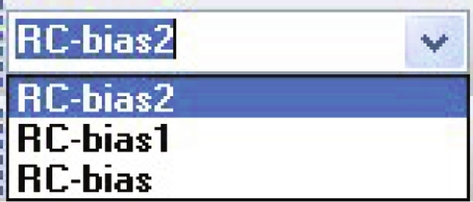
Note that bias2 is selected which appears in the Project Manager with a red icon to its left. This indicates that this is the current or active profile. You can select another profile in the pull down list or alternatively select the profile in the Project Manager and right mouse button (rmb) > Make Active.
12. Select bias1 in the pull down profile list in Fig. 2.34 and note the change in the Project Manager Simulation Profiles section. Bias1 is now the active profile.