Smoke Analysis
Abstract
Abstract
Smoke analysis gives an indication as to whether components are operating within manufacturer's absolute maximum ratings. Components that are continually operating close to maximum ratings can result in electrical and thermal stress leading to premature component failure. To provide for a margin of safety, manufacturer's maximum operating conditions can be derated to provide safe operating limits for components.
Keywords
Smoke; Capacitors; Stress; Voltages; Circuit; Resistor; Derating; Power dissipation
Smoke analysis gives an indication as to whether components are operating within manufacturer's absolute maximum ratings. Components that are continually operating close to maximum ratings can result in electrical and thermal stress leading to premature component failure. To provide for a margin of safety, manufacturer's maximum operating conditions (MOCs) can be derated to provide safe operating limits for components.
Smoke Analysis reports on stress-related parameters such as breakdown voltages, operating currents, device temperatures, junction temperatures, and power dissipations.
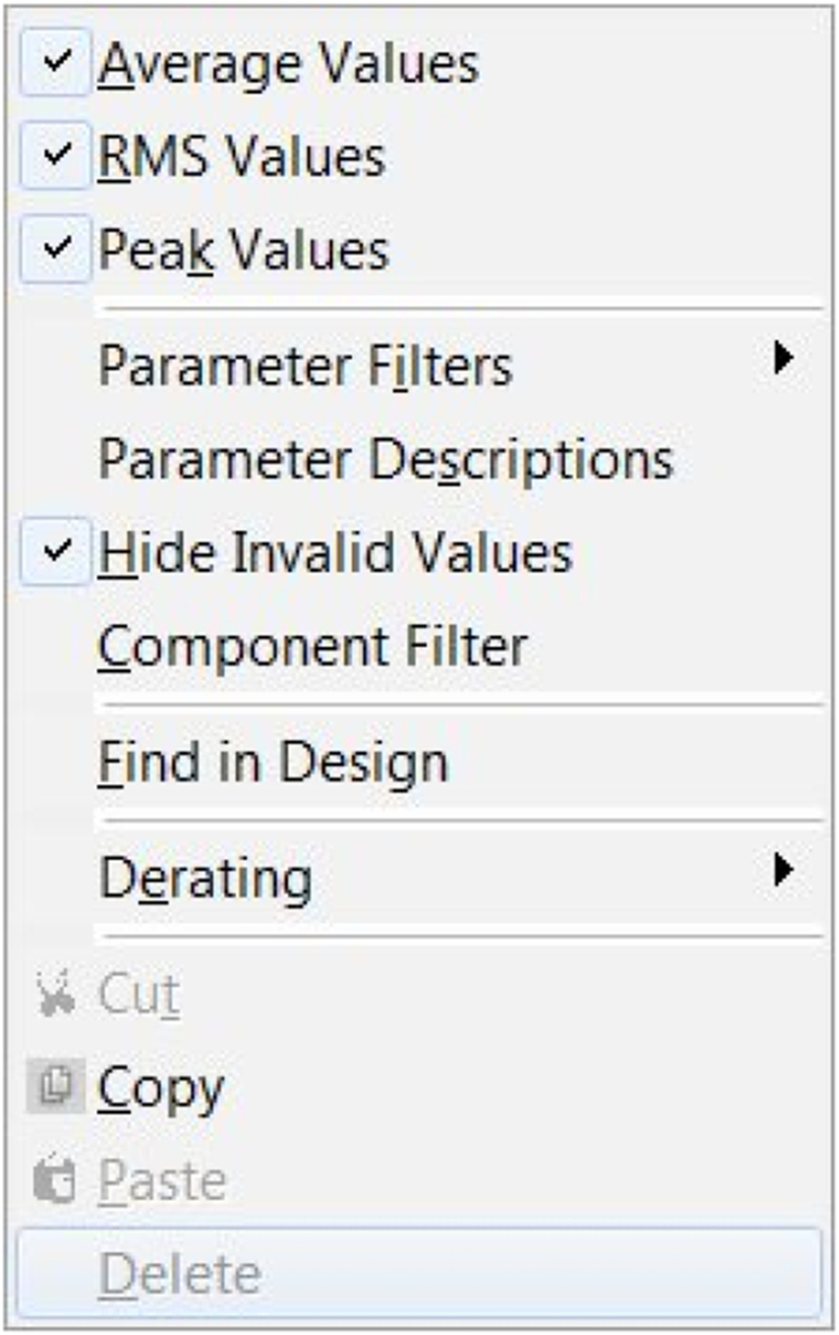
Fig. 27.1 shows the results of a Smoke analysis where the red bars indicate that the component Smoke limits are exceeding the MOCs. Orange bars indicate that the limits are > 90% of the MOCs and the green bars indicate that parameters are operating within 90% of the MOC.
Smoke analysis parameters allow MOCs to be defined for a component, the parameter values being those given in manufacturer data sheets. Advanced analysis contains libraries of components that already have Smoke parameters defined. However, in the latest Cadence 17.2 software release, Smoke parameters can be added to almost every device. For active components, Smoke parameter values can be entered via the PSpice Model Editor whereas for passive components, Smoke parameter values can be added to individual components or they can be added globally using the Design Variables part (Fig. 27.2).

The Assign Tolerance window, that displays all circuit components with tolerances and components with associated models, can also be used to open the PSpice Model Editor (see Fig. 27.3).
27.1 Passive Smoke Parameters
The passive components consist of resistors, capacitors, inductors, and power supplies placed from either the analog or pspice_elem libraries. All of these components are specified to operate over a given rated temperature range beyond which the output parameters have to be derated in order for the components to operate reliably with an increase in ambient temperature.
27.1.1 Resistor Smoke Parameters
Smoke Analysis calculates and displays the maximum power dissipation, maximum body temperature, and maximum voltage drop across a resistor.
A current flowing through a resistor will generate heat resulting in an increase in temperature that will affect the normal operation of the resistor. The maximum specified power rating for a resistor relates to the heat that can be dissipated up to a specified ambient temperature limit above which the operation of the resistor will degrade or fail. Beyond the temperature limit, the power that can be dissipated as heat decreases as a percentage of the maximum power rating. Fig. 27.4 shows the Derating Power curve for a resistor used in Smoke analysis.

The maximum power rating (POWER) for a resistor is specified over its normal operating ambient temperature range up to its rated temperature, TKNEE. Above this temperature, the power rating decreases at a rate given by the SLOPE, eventually falling to zero at the maximum temperature rating for a resistor, MAX_TEMP.
For example, a 0.25 W resistor is capable of dissipating a maximum power of 0.25 W up to a typical ambient temperature of 70°C. Exceeding the 0.25 W power rating of the resistor will result in excess heat that cannot be efficiently dissipated resulting in an increase in resistor temperature. Beyond 70°C, the effective power dissipation will decrease up to the maximum temperature typically 150–200°C at which point the resistor will fail. Premature resistor failure can be avoided by increasing the power rating of the resistor, increasing airflow across the resistor, using an equivalent parallel combination of resistors, using ventilated cases or to avoid placing resistors close to heat sources such as power transistors. Table 27.1 summarizes the resistor Smoke Analysis parameters.
Table 27.1
Resistor parameters used in Smoke Analysis
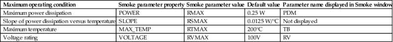
| Maximum operating condition | Smoke parameter property | Smoke parameter value | Default value | Parameter name displayed in Smoke window |
| Maximum power dissipation | POWER | RMAX | 0.25 W | PDM |
| Slope of power dissipation versus temperature | SLOPE | RSMAX | 0.0125 W/°C | Not displayed |
| Maximum temperature | MAX_TEMP | RTMAX | 200°C | TB |
| Voltage rating | VOLTAGE | RVMAX | 100V | RV |
In Smoke analysis, the resistor derating curve is defined by the KNEE temperature and the MAX temperature both of which are related by the SLOPE of the power derating curve. You can enter the SLOPE parameter value using the Variables symbol from which the KNEE value will be calculated. Alternatively, you can add the TKNEE property to the resistor using the Property Editor. See Example 1 at the end of the chapter.
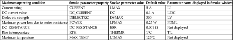
27.1.2 Inductor Smoke Parameters
Smoke Analysis displays the maximum DC current rating, maximum dielectric strength, maximum power loss due to equivalent series resistance (ESR) and inductor temperature rise.
Inductors are made from insulated coils of wire wound in air or wound on a ferrite magnetic core. When current flows through the wire windings, average real power is dissipated in the form of heat associated with the inherent DC resistance of the wire windings that make up the coils. Exceeding the inductor maximum DC current ratings can lead to saturation effects. The self-heating losses due to winding resistance will also cause a temperature rise in the inductor resulting in the wire insulation material to fail. Similarly, if the inductor maximum voltage ratings are exceeded, the insulation can also break down resulting in windings to short circuit and overheat. For core wound inductors and transformers, the current flowing through the inductor windings will generate heat resulting in an increase in temperature that will affect the magnetic characteristics of ferrite core materials. Core saturation levels decrease with an increase in temperature resulting in inductance values to decrease.
Subsequently, manufacturers specify the maximum inductor current rating (DC) and maximum voltage rating over a maximum ambient temperature range for reliable operation. Smoke analysis does not calculate the derating of inductor current with temperature.
The power dissipated by the inherent DC resistance of the inductor is attributed to the average current flowing through the inductor resulting in a temperature rise above ambient. Manufacturers specify the average current as an Irms current that causes a maximum allowable rise in temperature by a specified value above the ambient temperature. Hence, the maximum ambient temperature and maximum allowable temperature rise define the inductor maximum temperature MAX_TEMP.
Inductors also specify a rated saturation current (Isat) that is associated with the saturation of the inductor core resulting in the inductance value to decrease. Smoke analysis supports four parameters associated with inductors: DC current for saturation, temperature rise, breakdown voltage, and MAX current. See Example 2 at the end of the chapter. Table 27.2 lists the inductor Smoke parameters.
Table 27.2
Inductor Smoke Analysis parameters
| Maximum operating condition | Smoke parameter property | Smoke parameter value | Default value | Parameter name displayed in Smoke window |
| Current rating | CURRENT | LMAX | 5 A | LI |
| DC current value | DC_CURRENT | DC | 0.1 A | LIDC |
| Dielectric strength | DIELECTRIC | DSMAX | 300 | LV |
| Maximum power loss due to series resistance | POWER | LPMAX | 0.25 W | PDML |
| DC_RESISTANCE | DC_RESISTANCE | ESR | 0.001 Ω | Not displayed |
| Rise in temperature | RTH | THERMR | 1°C | TJL |
| Maximum temperature | MAX_TEMP | LTMAX | 125°C | Not displayed |
The ESR property is not available on the standard inductor from the analog.olb library. You have to use the L_t from the analog.olb.
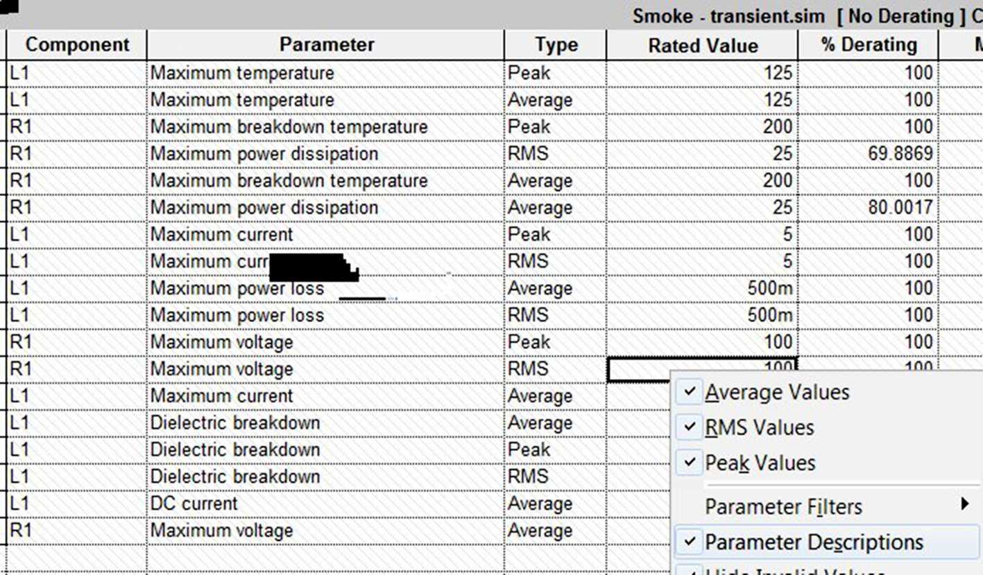
Tip
When you run Smoke analysis, the Parameter names are shown in short form. To see the complete description, rmb > Parameter Descriptions as shown in Fig. 27.5.
27.1.3 Capacitor Smoke Parameters
Smoke Analysis calculates and displays the maximum rated voltage, maximum ripple current, maximum reverse voltage, maximum ESR power dissipation and capacitor temperature rise.
Applied voltage as well as temperature affects the reliability of a capacitor and its initial power on performance. The range of ambient temperature over which a capacitor can continuously operate is known as the category temperature range and is defined by upper and lower temperature limits. The rated temperature (upper category limit) is defined as the maximum ambient temperature that a capacitor can operate continuously without exceeding the rated voltage. Exceeding the capacitors maximum voltage rating will cause the dielectric to break down. Subsequently, manufacturers provide voltage derating guidelines to improve the long-term reliability of their capacitors. Fig. 27.6 shows the voltage-temperature derating curve for a capacitor used in Smoke analysis.

The rated VOLTAGE is the maximum peak DC operating voltage that can be applied to a capacitor for continuous operation, also known as the working voltage that appears printed on the capacitor. The rated temperature, KNEE is the maximum ambient temperature over which the capacitor can continuously operate at the rated VOLTAGE. The maximum ripple current is the AC rms current that flows in and out of a capacitor and it is this current that produces heat and hence power dissipation (PDML) in the ESR. Smoke analysis supports electrolytic and nonelectrolytic capacitors. The CVN parameter is used to report on short reverse transient voltages. The maximum ambient temperature at which the capacitor can operate is given by MAX_TEMP. Table 27.3 summarizes the capacitor parameters used in Smoke analysis.
Table 27.3
Capacitor parameters used in Smoke analysis
| Maximum operating condition | Smoke parameter property | Smoke parameter value | Default value | Parameter name displayed in Smoke window |
| Maximum ripple | CURRENT | CIMAX | 1 A | CI |
| Voltage Rating | VOLTAGE | CMAX | 50 V | CV |
| Maximum reverse voltage | NEGATIVE_VOLTAGE | CVN | 10 V | CVN |
| Maximum power loss due to series resistance | POWER | CPMAX | 0.1 W | PDML |
| Temperature derating slope | SLOPE | CSMAX | 0.005 V/°C | Not displayed |
| Breakpoint temperature | KNEE | CBMAX | 125°C | Not displayed |
| Rise in temperature | RTH | THERMR | 1°C | TJL |
| Maximum temperature | MAX_TEMP | CTMAX | 125°C | Not displayed |
| Equivalent series resistance | ESR | ESR | 0.001 Ω | Not displayed |

The rated temperature is different for capacitors with different dielectrics. Electrolytic aluminum and tantalum capacitors have a working voltage dependence on temperature compared to nonelectrolytics such as ceramic, polyester, and other plastic film capacitors. Capacitance and leakage current are also dependent on temperature. Smoke analysis supports electrolytic and nonelectrolytic capacitors and will test for reverse transient voltages. The CVN parameter defines the negative voltage ratings.
27.2 Active Smoke Parameters
Smoke analysis incorporates parameters for semiconductor devices that include diodes, diode bridge rectifiers, zener diodes, bipolar transistors, JFET, MESFET, MOSFET, power MOSFET, dual MOSFET, IGBT, LED, optocouplers, varistors, and thyristors.
27.2.1 Bipolar Transistors
Bipolar transistors used in power amplifiers or power switching circuits should be operated within their safe operating area in order to avoid excessive power dissipation that can lead to premature failure. Manufacturers provide derating curves that plot maximum continuous power dissipation against collector junction temperature also known as case temperature. For silicon transistors, the range is normally specified from room temperature at 25°C to 150°C.
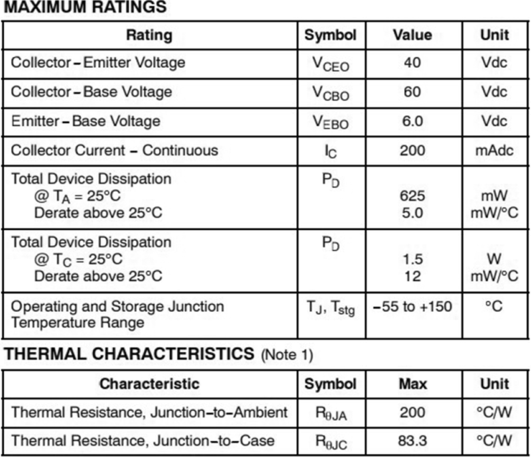
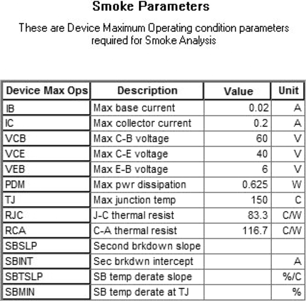
The power derating curve for a transistor is shown in Fig. 27.7. The transistor case temperature is related to the collector-base junction temperature (TJ). The transistor junction thermal (ΘJA) resistance is composed of the junction-to-case thermal resistance (RJC) that is a fixed value and the case-to-ambient thermal resistance (RCA). The case-to-ambient thermal resistance can be decreased by using a heatsink that effectively increases the surface area of the transistor case. In the case of power transistors, the collector-base junctions have large areas in order to dissipate heat quickly away from the junction. Table 27.4 lists the Smoke analysis parameters used for bipolar (BJT) transistors.
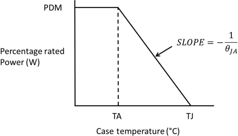
Table 27.4
Bipolar parameters used in Smoke analysis
| Semiconductor component | Maximum operating condition | Smoke parameter name property and symbol property name | Parameter name displayed in Smoke window |
| BJT | Maximum base current (A) | IB | IB |
| BJT | Maximum collector current (A) | IC | IC |
| BJT | Maximum power dissipation (W) | PDM | PDM |
| BJT | Thermal resistance, Case-to-Ambient (°C/W) | RCA | Used for calculating junction temperature |
| BJT | Thermal resistance, Junction-to-Case (°C/W) | RJC | Not displayed |
| BJT | Secondary breakdown intercept (A) | SBINT | Not displayed |
| BJT | Derated percent at TJ (secondary breakdown) | SBMIN | Not displayed |
| BJT | Secondary breakdown slope | SBSLP | Not displayed |
| BJT | Temperature derating slope (secondary breakdown) | SBTSLP | Not displayed |
| BJT | Maximum junction temperature (°C) | TJ | TJ |
| BJT | Maximum collector-base voltage (V) | VCB | VCB |
| BJT | Maximum collector-emitter voltage (V) | VCE | VCE |
| BJT | Maximum emitter-base voltage (V) | VEB | VEB |

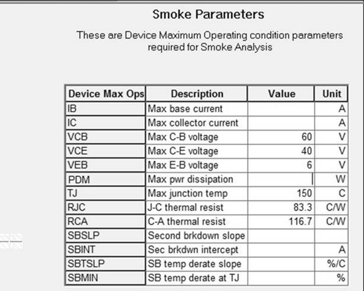
Semiconductor smoke analysis parameters are defined in the semiconductor PSpice models. The smoke parameters can be viewed using the PSpice Model Editor that can be accessed either from the circuit diagram or from the Start Menu. In the circuit diagram you highlight the transistor part and rmb > PSpice Model Editor. See Example 4 at the end of the chapter. Fig. 27.8 shows the Smoke parameters and their values for a Q2N3904 transistor.
The other semiconductor types and their associated Smoke parameters can be found in the online PSpice Advanced Analysis User Guide.
27.3 Derating Files
As well as providing MOCs, many manufacturers provide derating guidelines for their components so they can operate within safe operating limits (SOL) that is given by
For example, using a derating of 75% on the Vmax of a 200 V capacitor, Smoke Analysis will indicate any excursions > 150 V in the form of a red bar in a bar graph display.
You can also define different deration specifications for each of the supported device types. This allows you to define a unique deration margin for each specification and associate this to an instance in the circuit diagram. For example, you can have two different derating definitions for MOSFET drain currents. A derating margin of 50%, say for use in high reliability products otherwise a derating margin of 70% for all other designs. These derating specifications can be stored in global files for reuse in other circuit designs.
Smoke Analysis comes with standard passive and active derating factors that can be found in the standard.drt file in the tools > PSpice > Library folder:
C:CadenceSPB_17.2 oolspspicelibrary
The standard.drt file can be opened with a text editor. However, it is easier to use Advanced Analysis using the Profile Settings window, Edit > Profile Settings. You can then browse to the default standard.drt derating file by clicking on New (Insert) as shown in Fig. 27.9. Cadences also supply a custom_derating_template file that can be modified to create new derating files.
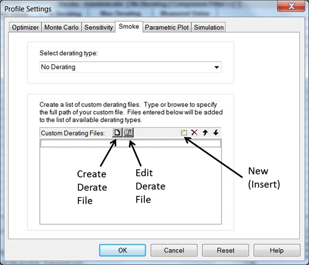
Selecting either Create Derate File or Edit Derate File opens up the Edit Derate File window (Fig. 27.10) where you can enter the smoke parameters. You can build up a collection of derating files that will be displayed in the Profile Settings windows. The files will then appear in a pull down box under Select derating type.
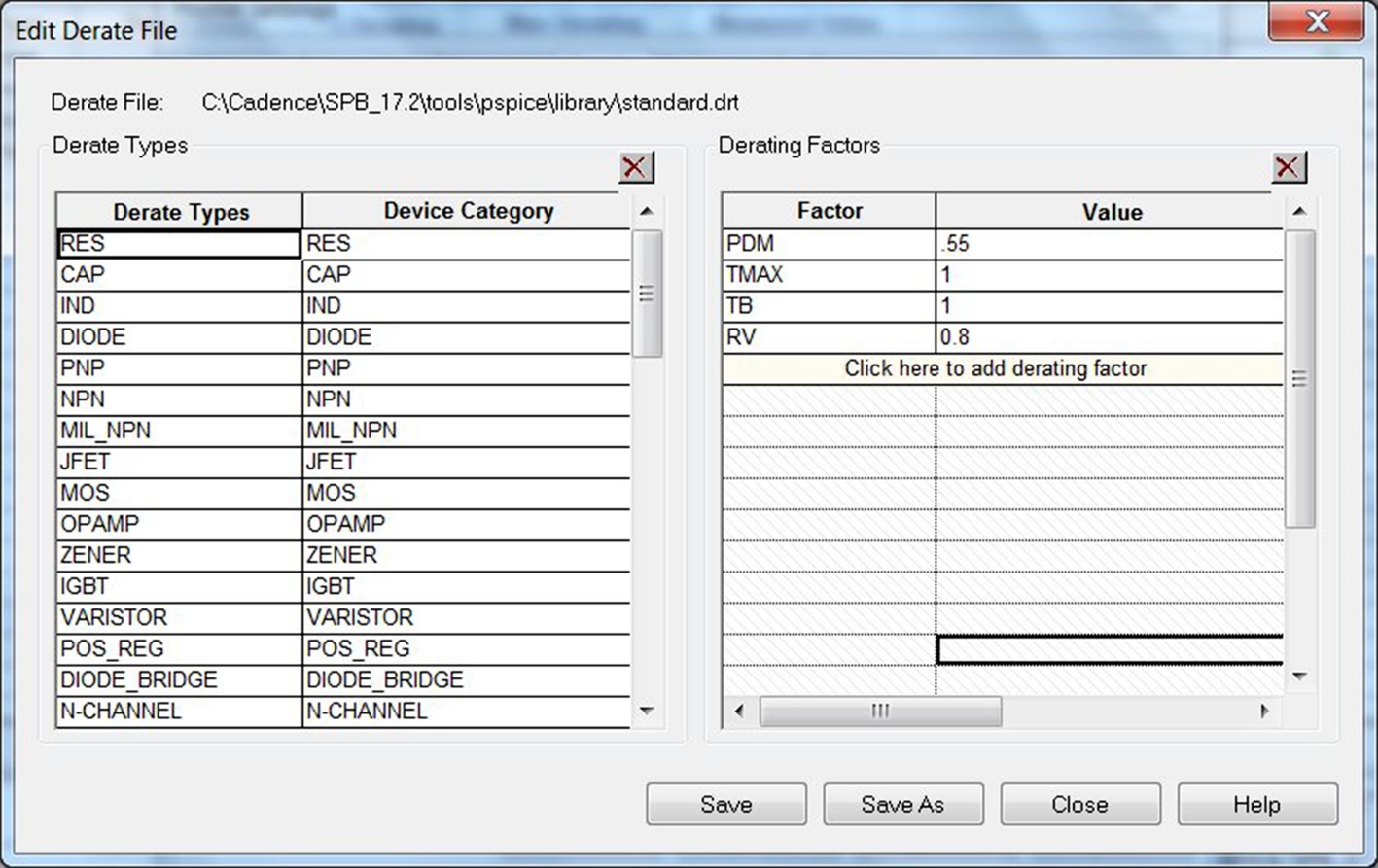
Fig. 27.10 shows the default derating factors using the Smoke Analysis “standard derating” file. When you select “Standard Derating” in Smoke Analysis, all the derating factors will be applied to the components. For example, a derating factor of 0.55 will be applied to the maximum power (PDM) rating of the resistors. PDM is the same as RMAX. If the calculated power exceeds the derated value then a red bar indicates that the power has exceeded the derated value and by how much (see Fig. 27.11).
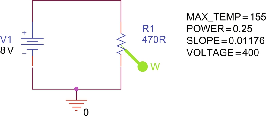
27.4 Example 1
Fig. 27.12 shows the power-temperature derating curve for a 470 kΩ metal film resistor. The corresponding specifications from the manufacturer's data sheet are given as:

Rated Power @70°C (W) 0.25 W
Max overload voltage 400 V
Operating temperature range − 55°C to + 155°C
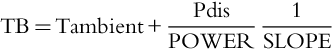
The resistor body temperature, TB is given by
where ΔT is the temperature rise due to the self-heating effect of the ESR and subsequent power dissipation.
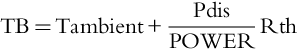
where
Tambient—ambient temperature that has a default value of 27°C set by TNOM
Rth—resistor to ambient thermal resistance
Pdis—calculated power dissipation
POWER—maximum rated power dissipation
Rth = 1/SLOPE and Pdis is calculated from the result of running a transient analysis.
As manufacturer's derating curves show unit power derating, the slope RSMAX is given by
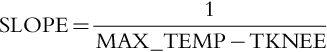
where MAX_TEMP is the maximum operating temperature.
From Eq. (27.5), TKNEE can be calculated as:
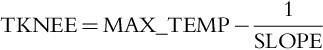
Combining Eqs. (27.4), (27.5):

If TKNEE is not known, the derating slope is used to calculate TB using Eq. (27.3) else if TKNEE is known then Eq. (27.7) can be used to calculate TB. The TKNEE property can be added to individual resistors.
Therefore,
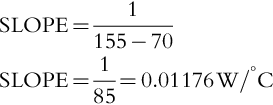
Therefore the Smoke parameters defined in Table 23.1 are
MAX_TEMP, RTMAX = 155
SLOPE, RSMAX = 0.01176
VOLTAGE, RVMAX = 400
Fig. 27.13 shows the resistor circuit with Smoke parameters added. From the results of a transient analysis, power dissipation Pdis was calculated as 136.17 mW.
From Eq. (27.3), the resistor body temperature is given by
Derating Factor
From the derating curve in Fig. 27.12, if the resistor body temperature exceeds TKNEE, the power dissipation will be dynamically derated by a Power Derating Factor, PDF given by
From which the derated power is given by
The standard derating file for a resistor in Smoke Analysis is 0.55. Therefore the derated power is given by
27.5 Exercises
Exercise 1
1. Create a new PSpice project called for example Smoke_Resistor and in the Create PSpice Project window, select simple_aa.opj from the pull-down menu (Fig. 27.14).

2. Delete the AA Variables part. Draw the resistor circuit in Fig. 27.15.
3. Double click on the resistor to open the Property Editor and add the following Smoke Limit parameters values:
MAX_TEMP = 155
SLOPE = 0.01176
POWER = 0.25
VOLTAGE = 400
No need to enter the SI units.
To display the Smoke limits, highlight each Smoke parameters by holding down the control key and clicking on each property. Select Display (or rmb > Display) and in the Display Properties window, select Name and Value as shown in Fig. 27.16.

4. Set up a transient analysis (PSpice > New Simulation Profile) and leave the default Run To Time as 1000 ns.
5. Place a Power marker on the body (middle) of the resistor. PSpice > Markers > Power Dissipation or click on the icon  .
.
6. Run the simulation.
7. The Probe window in PSpice window will appear displaying a power dissipation trace of 136.170 mW.
8. Go back to Capture and select, PSpice > Advanced Analysis > Smoke.
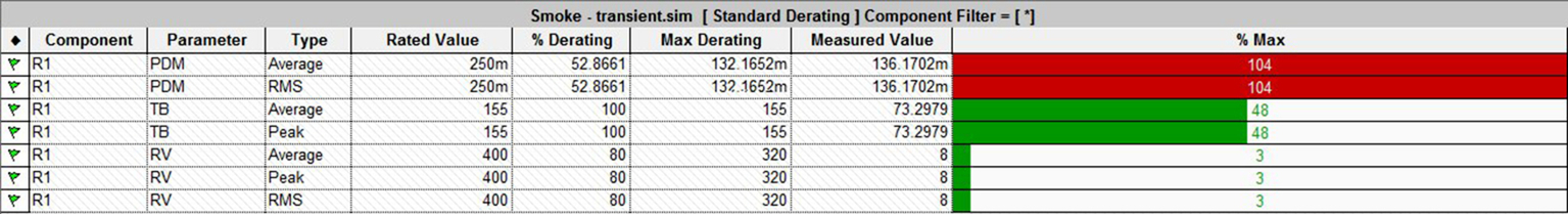
9. PSpice Advanced Analysis will open up showing the results of the Smoke Analysis. Invalid values will be displayed as gray bar lines. For example, only average and peak values are calculated for TB, the RMS value is invalid. Right mouse click anywhere and select Hide Invalid Values. Fig. 27.17 shows the results of the Smoke Analysis with a power dissipation calculated as 136.1702 mV.

% Max is given by: 100 × 136.1702 m/240.3004 m = 57%.
10. Using Eq. (27.3) the resistor body temperature is calculated as TB = 73.3163°C. Obviously Smoke Analysis uses a greater number of significant digits in the calculations. A more accurate “hand” calculation would be to use 1/SLOPE = 85 rather than use SLOPE = 0.01176. This gives the same result as Smoke Analysis as 73.2978°C.
11. The resistor body temperature of 73.2978°C is greater than the TKNEE temperature of 70°C and so the power dissipation is dynamically derated. The value of the derating factor (% Derating) is given by Eq. (27.8) as:
For a more accurate calculation:
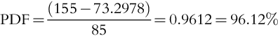
Therefore using Eq. (23.9), the power dissipation (Max Derating) is given by
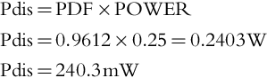
This is the value of PDM shown in Fig. 27.17.
12. Right mouse click anywhere in Smoke Analysis and select Derating > Standard Derating and run the simulation by clicking on the play button.
13. You should see two red bars that indicate that the derated values for PDM (RMAX) have been exceeded by 104% Fig. 27.18. The resistor is not operating within the defined safe operating limits.
14. In Capture, change the value of POWER to 0.5.
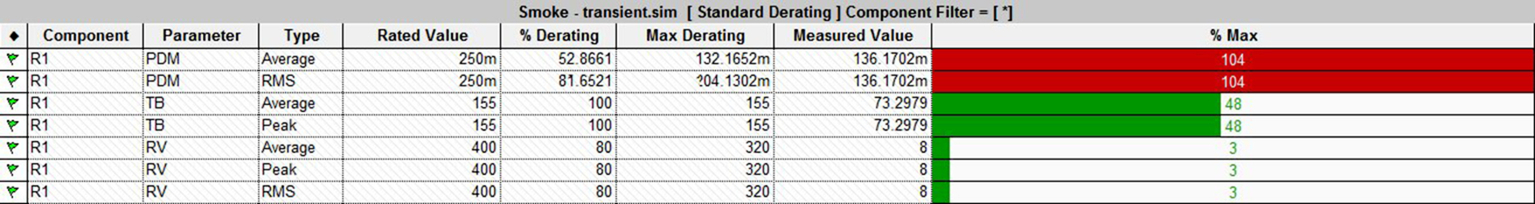
15. Re-run the transient simulation and then run Smoke Analysis. You will see that using a 0.5 W resistor, the power dissipation of the resistor (Fig. 27.19) meets the defined safe operating limits of operation. In fact you could even use a 0.4 W resistor.
27.6 Example 2
Fig. 27.20 shows the temperature rise characteristics curve for the Murata 1.5 μH Inductor LQM2HPN1r5MG0, respectively.

Specification for a Murata 1.5 μH Inductor are given as:
Temperature range: − 55°C to + 125°C
Rated temperature TR = 85°C
1.5 A @ambient temperature 85°C
1.1 A @ambient temperature 125°C
The inductor temperature, TJL is given by the sum of the ambient temperature and inductor temperature rise ΔT:
For example, an inductor specifies the maximum current rating up to a typical ambient temperature of 85°C and a maximum allowable temperature rise of 40°C. The maximum operating temperature is therefore 125°C.
The temperature rise ΔT associated with the power dissipation of the inductor DC resistance is given by
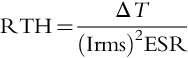
RTH is the inductor thermal resistance and Pdis is related to the average real power dissipated by the inductor resistance given by
Therefore (23.10) can be written as:
Inductor thermal resistances (RTH) are not normally specified by manufacturers as the value of RTH is dependent on how the inductors are mounted on circuit boards. However, some manufacturers specify different current ratings for surface mount inductors using different PCB mountings and land pattern areas. Thermal resistances are not usually specified for frame core inductors and transformers as the thermal resistance paths are not clearly defined. However, the thermal resistance can be approximated using the manufacturer's specified Irms current.
From Eqs. (23.11), (23.12), the inductor thermal resistance can be calculated as:
where ΔT is a specified temperature rise at a given Irms current. From the graph of Temperature Rise versus Current (Fig. 27.19), Irms = 2.4 A @40°C. The inductor thermal resistance is therefore calculated as:
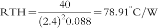
Fig. 27.21 shows the inductor circuit with added Smoke parameters. The result of a transient analysis calculates the Irms as 1.0606 A. From Eq. (27.12):
Using Eq. (27.14), the inductor temperature is
Exercise 2
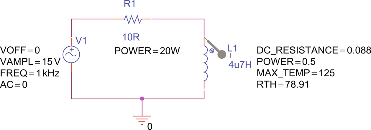
1. Create a new PSpice project called Smoke_Inductor and in the Create PSpice Project window, select simple_aa.opj from the pull-down menu (Fig. 27.22).
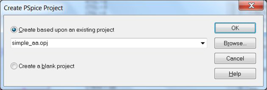
2. Draw the inductor circuit in Fig. 27.23. Use an L_t inductor from the analog library as this has the ESR property attached. Place a VSIN source from the source library.
3. Double click on the resistor and in the Property Editor for POWER, set RMAX to 20 W. To display the power value 20 W, click on Display > Name and Value. Close the Property Editor.
4. Double click on the inductor to open the Property Editor and add the following Smoke Limit parameters values:
DC_RESISTANCE = 0.088
MAX_TEMP = 125
RTH = 78.91
POWER = 0.5
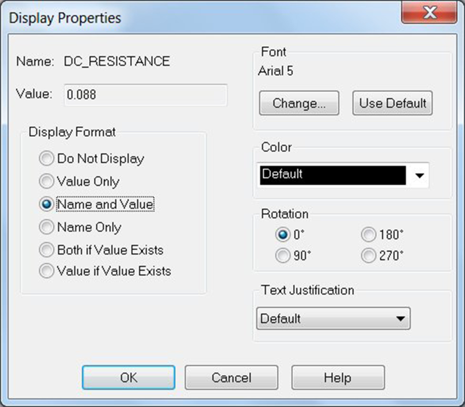
Highlight each Smoke parameters by holding down the control key and clicking on each property. Select Display and in the Display Properties Window select Name and Value (see Fig. 27.24).
5. Set up a transient analysis with a Run To Time of 4 ms.
6. Place a Current marker on pin1 of the inductor that is marked with the dot symbol. Run the simulation.
7. The Probe window in PSpice window will appear displaying the inductor current with a max value (LI) of 1.4942 A.
8. Go back to Capture and select, PSpice > Advanced Analysis > Smoke.
9. PSpice Advanced Analysis will open up showing the results of the Smoke Analysis for the resistor R1 and inductor L1. Invalid values will be displayed as gray bars. For example, only average and peak values are calculated for TJL. Right mouse click anywhere and select Hide Invalid Values (Fig. 27.25).

You should see the results in Fig. 27.26.

10. It is always a good idea to have a look at the Smoke Analysis log file. View > Log File > Smoke as shown in Fig. 27.27.
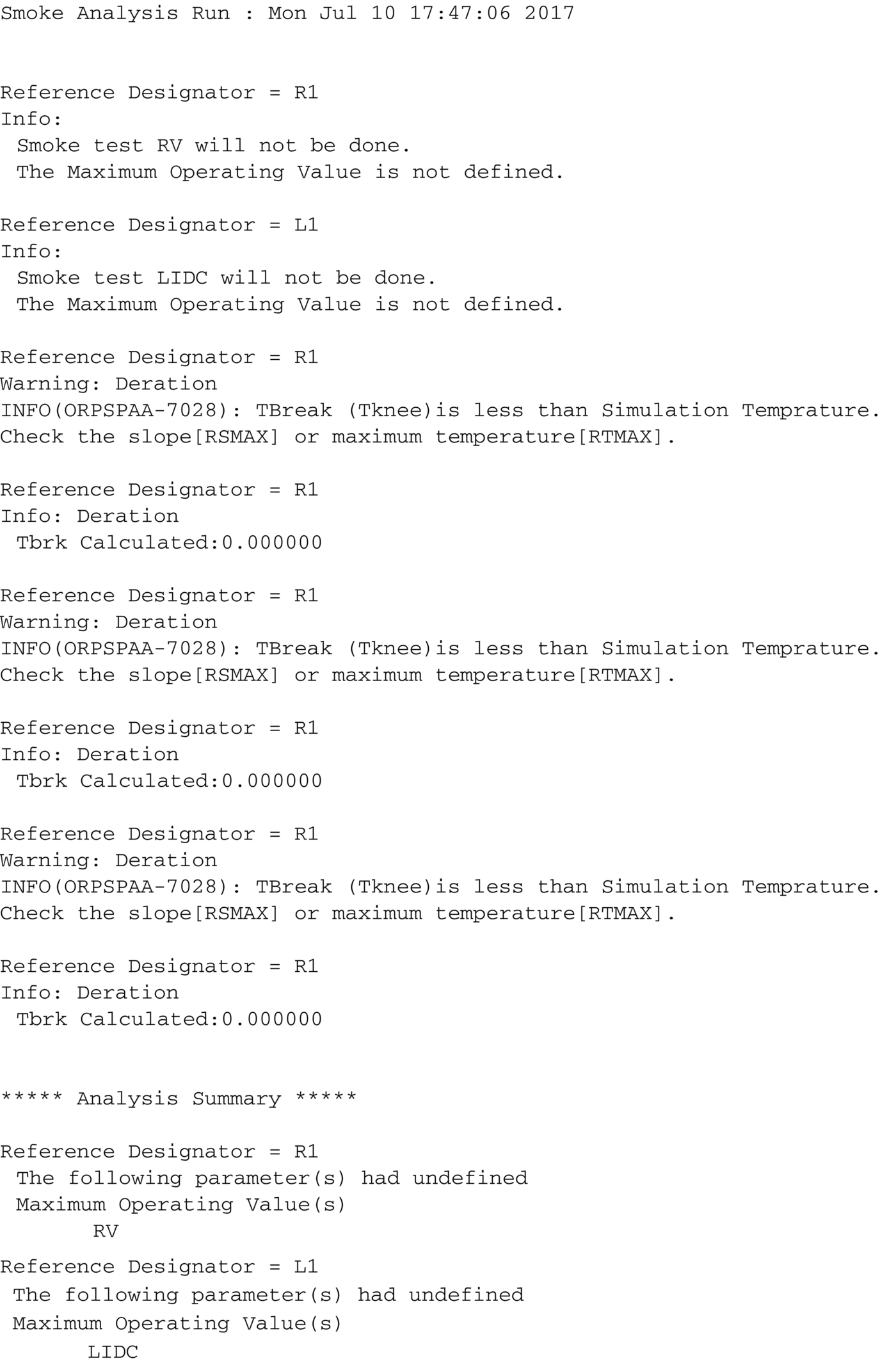
11. The log file in Fig. 27.27 reports undefined CV parameter for R1 and an undefined parameter LIDC for L1. A warning message reports on TKNEE being less than the simulation temperature and to check the values for the SLOPE and MAX_TEMP. These values were not added on the resistor and so default values were used.
12. In Capture double click on the resistor to open the Property Editor. Set the limit of MAX_TEMP (RTMAX) to 155 and the VOLTAGE limit (RVMAX) to 200. Do not close the Property Editor.
Rather than calculate the SLOPE, you can set the TKNEE limit. Select New Property and add TKNEE as shown in Fig. 27.28.

13. Re-run the simulation in Capture.
14. Re-run Advanced Analysis and look at the Smoke Analysis log file (Fig. 27.29).

15. Select the inductor and set the DC_Current limit (DC) to 1 A. As shown in Table 27.2, Smoke Analysis displays the DC_Current as LIDC.
16. Re-run the PSpice simulation in Capture.
17. Re-run Advanced Analysis.
18. The results for the resistor and inductor are displayed. Right mouse click anywhere and select Component Filter. The default wildcard setting (⁎) displays all components. As shown in Fig. 27.30, enter L1 and click on OK.

19. Fig. 27.31 shows the results of the Smoke Analysis for the inductor only.

The current LIrms is 1.0604 A
Therefore from Eq. 27.12 the approximate value for Pdis is
The average inductor temperature is given by
However, the values are shown with no derating.
20. In Smoke Analysis, select Edit > Profile Settings and in the Profile Settings window, click on the New (Insert) icon as shown in Fig. 27.32. Click on three ellipses (…) and browse to the default standard.drt derating file in the; < install path > oolspspicelibrary. For example:

C:CadenceSPB_17.2 oolspspicellbrary
21. Click on the Edit Derate File to display the Derate Types and Derating Factors (Fig. 27.33). Maximum power dissipation (PDM) is derated to 0.55 and voltage rating (RV) is 0.8.

22. Select the inductor (IND) and you will see that LI, LV, and LIDC all have a derating factor of 0.9.
23. Close both the Edit Derate File and Profile Settings windows.
24. Right mouse click anywhere in Smoke Analysis and select Component Filter and enter ⁎ to select all components.
25. Again, right mouse click anywhere in Smoke Analysis but this time select Derating > Standard Rating. Run Smoke analysis again. You will see two red lines indicating that the derated resistor power has been exceeded.
26. Change the resistor power in Capture to 30 W and re-run the PSpice simulation and then the Smoke Analysis. The final Smoke Analysis is shown in Fig. 27.34.

27.7 Example 3
The datasheet for a 1 μF plastic film, polyethylene terephthalate (PET) capacitor gives
Rated temperature TR—85°C
Derating factor—1.25% per °C
Maximum temperature—125°C
Dissipation factor of 0.004 @ 1 kHz
Rated voltage—50 VDC
The ESR is not given in the datasheets, so it can be calculated from
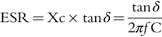
where
tanδ—dissipation factor, DF
f—test frequency, typically 120 Hz
C—capacitance
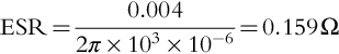
Therefore the equivalent series resistance is
The capacitor temperature, TJL is given by
where ΔT is the temperature rise due to the self-heating effect of the ESR and subsequent power dissipation and is given by
Rth is the capacitor thermal resistance and Pdis is related to the average real power dissipated by the capacitor's ESR. Power dissipation is attributed to the AC Irms ripple current that flows in and out of a capacitor producing internal heating effects. Ignoring the effects of the leakage current, the power dissipation in the ESR is given by
Therefore the rise of capacitor temperature is given by
The thermal resistance of the capacitor, Rth, is given by the reciprocal of the SLOPE from the voltage derating curve and I2rms is calculated from the result of running a transient analysis.
If the capacitor thermal resistance is not specified in manufacturer's datasheets, the SLOPE can be calculated from
Therefore Eq. (27.22) can be written as:

Where CTMAX is the maximum operating temperature and TKNEE is the rated temperature that a capacitor can operate continuously without exceeding the rated voltage, also known as the upper category temperature.
For this example both the slope and TKNEE are given. Only the TKNEE value will be used.
MAX_TEMP, CTMAX = 125
SLOPE, CSMAX = 0.0125
VOLTAGE, CMAX = 50
ESR = 0.159
Exercise 3
The voltage tripler circuit in Fig. 27.35 is used to demonstrate how Smoke analysis can be used to improve circuit performance by detecting components that do not meet the derated MOCs.
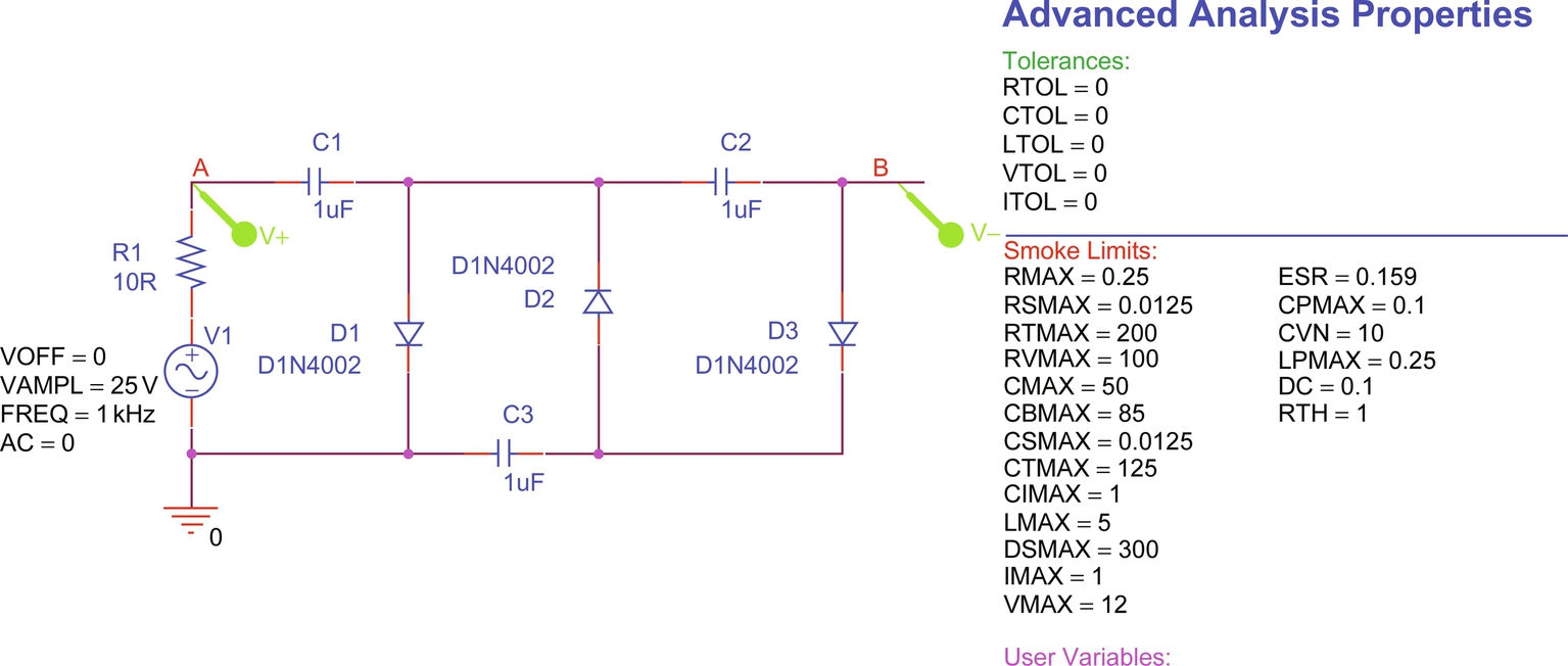
1. Create a new project called, for example, voltage_tripler. After you name the project, the Create PSpice Project window appears. In the pull-down menu select the simple_aa.opj and click on OK (Fig. 27.36).

2. Draw the voltage_tripler circuit in Fig. 27.35 Use a C_t capacitor from the analog library as this has the ESR property attached.
3. Add SMOKE parameter values to the Variables part as shown in Fig. 27.35.
4. Set up a transient analysis with a Run To Time of 50 ms.
5. Place a differential voltage marker on node A and B, PSpice > Markers > Voltage Differential. When you place the first V + marker, the second V − marker appears automatically. Alternatively, click on the icon  .
.
6. Run the simulation.
7. The Probe window in PSpice window will appear displaying the differential voltage between nodes A and B.
8. In PSpice, select View > Measurement Results and in the Measurement Results window, check on the box for Max(V(A)-V(B)) that will display a value of 73.25649 V, see Fig. 27.37.

9. Go back to Capture and select, PSpice > Advanced Analysis > Smoke.
10. PSpice Advanced Analysis will open up showing the results of the Smoke Analysis for the voltage_tripler circuit. Invalid values will be displayed as gray bar lines. For example, only average and peak values are calculated for TJL. Right mouse click anywhere and select Hide Invalid Values Fig. 27.38.
11. Right mouse click anywhere again and select Component Filter and enter C⁎ as shown in Fig. 27.39.

12. Fig. 27.40 shows the results of the Smoke Analysis for the voltage_tripler circuit.

The capacitor ripple current is given by PDML (rms) for capacitor C1 and is shown as 43.5728 μA. Therefore from Eq. (27.20) the approximate value for Pdis is
This small power dissipation is attributed to the small ESR value and is not going to change the capacitor temperature significantly. What is of more interest is the voltage rating for the capacitors. The yellow bar lines indicate that the voltage ratings are within 90% of their maximum ratings.
13. Right mouse click anywhere and select Derating > Standard Derating and run the Smoke analysis simulation.
14. You should see the results as shown in Fig. 27.41 where the red bars indicate that the derated MOCs have been exceeded.

15. Capacitors with a higher working voltage of 63 V can be used instead. Globally change the value of CMAX from 50 to 63 V and run the PSpice simulation and then the Smoke analysis simulation. You should see that the derated MOCs for the capacitors have not been exceeded.
27.8 Example 4
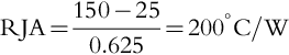
Transistor datasheets normally give two values for device power dissipation, one for ambient temperature and one for case temperature. Two values are also given for thermal resistances (Rth): junction to ambient and junction to case. If you use a heatsink, then the thermal resistance from junction to ambient is given by the sum of the transistor junction to case and heatsink thermal resistances. With no heatsink, the thermal resistance is given by the value of the transistor junction to ambient (see Fig. 27.42).
With no heatsink, transistor thermal resistance is given by Rja.
Transistor temperature is given by
where ΔT is given by
Hence
where Pdis is the calculated power dissipation from the result of a transient analysis. If there is no heatsink, the thermal resistance RTH is given by RJC + RCA.
where
RJC—junction-to-case thermal resistance
RCA—case-to-ambient thermal resistance
Therefore,
1. Use the voltage regulator circuit that was used in Sensitivity analysis. Otherwise draw the circuit in Fig. 27.43.

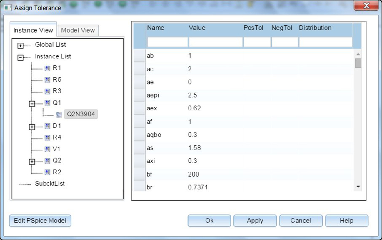
2. You need to edit the Smoke parameters for Q1 using the PSpice Model Editor. In the later 17.2 versions, you can open and edit the Smoke parameters via the Assign Tolerance window. Either way, you will be using the PSpice Model Editor to assign Smoke parameters. Either:
(a) Highlight Q1 > 2N3904 and rmb > Edit PSpice Model.
OR
(b) Select PSpice > Advanced Analysis > Assign Tolerance, select Q1 > 2N3904 then click on Edit PSpice Model.
3. Enter the Smoke Parameter values as shown in Fig. 27.44. If the Smoke Parameters are not shown in the Model Editor, then select View > Model.
Save the file and close the PSpice Model Editor.
4. Place a voltage marker on node “out” and a current marker on the bottom pin of load resistor R4.
5. Run a transient analysis using the default Run To Time of 1000 ns.
6. In PSpice set up two measurement expressions for V(out) and I(R4). Trace > Evaluate Measurement.
Select Max(1) from the Functions or Macros and then select V(out).
Select Max(1) from the Functions or Macros and then select I(R4).
See Fig. 27.45.

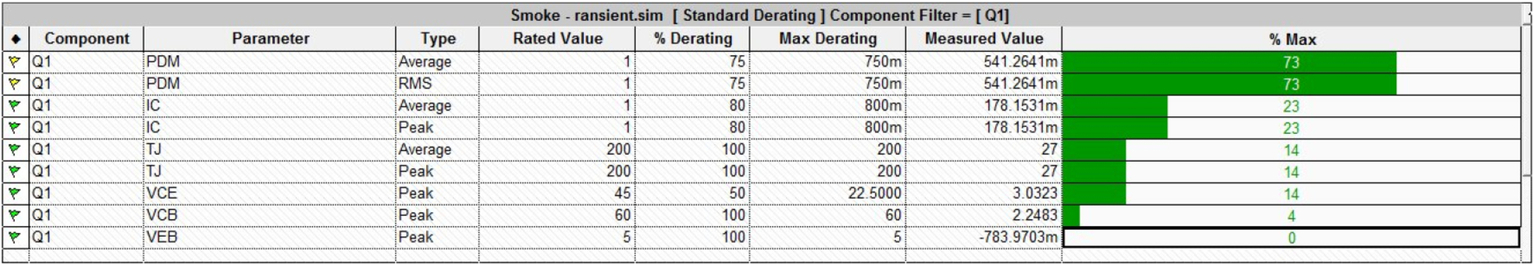
7. Return to Capture and select PSpice > Advanced Analysis > Smoke. RMB anywhere in the window and select > Hide Invalid Values. You should see the results in Fig. 27.46.
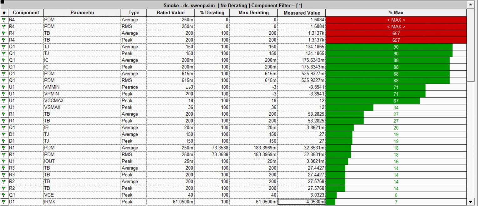
The results of the Smoke analysis give an average power dissipation for Q1 of 535.9327mW. There is no heatsink so using:
In Smoke analysis, the Rated Value of PDM is shown as 615 mW although the Smoke PDM parameter for the 2N3904 transistor was set at 625 mW in the Model Editor. Using the PDM value from the 2N3904 datasheet, the transistor junction thermal resistance is given by
where
TJ—maximum operating junction temperature
Ta—ambient temperature
RJA—junction thermal resistance (RJC + RCA)
However, the nominal simulation temperature TNOM that represents Ta is set at 27°C. Therefore using RJA = 200°C/W, the PDM displayed in Smoke analysis is given by
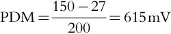
Smoke analysis will use the smallest PDM value.
8. From Fig. 27.46, the transistor temperature is within 90% of its maximum value.
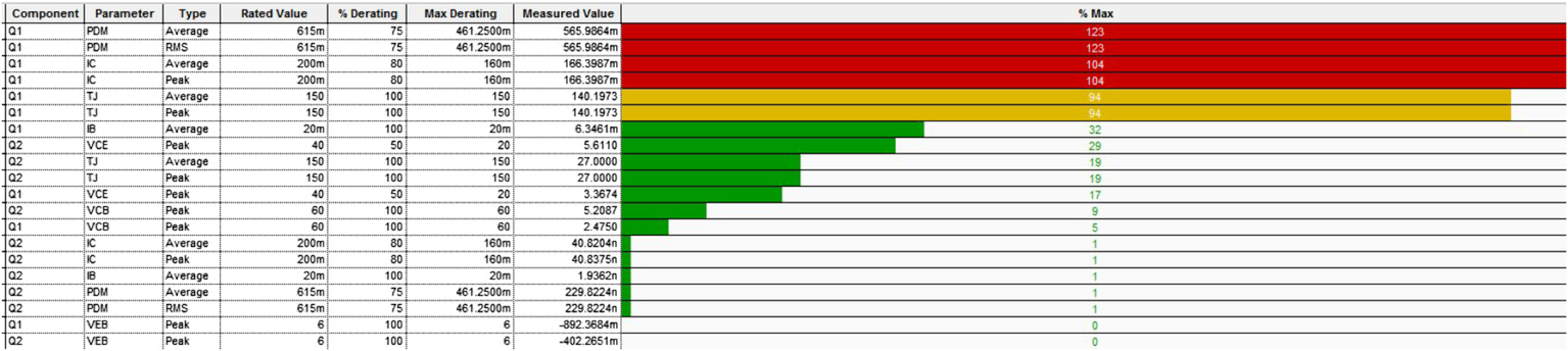
9. Click anywhere in the window and rmb > Derating > Standard Derating. Run the Smoke simulation again. You should see the results in Fig. 27.47.
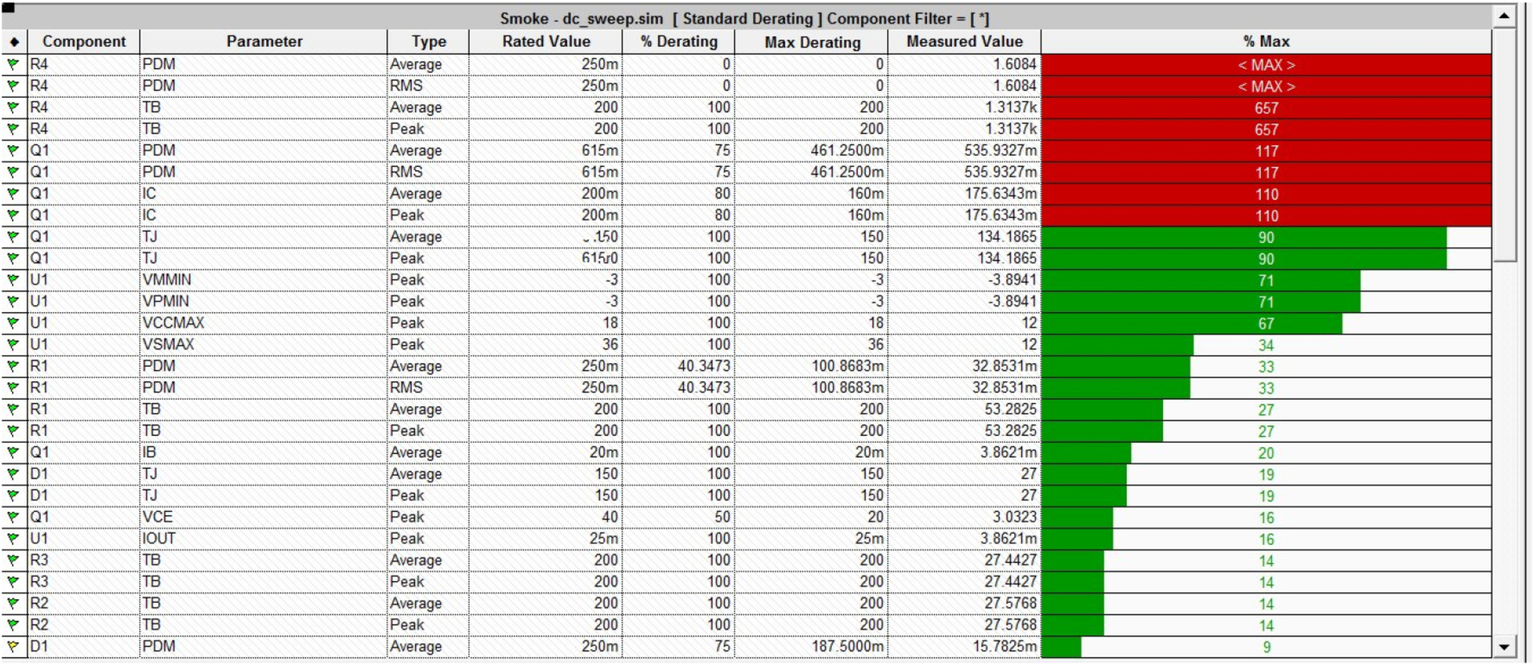
You need to use a transistor with a higher power dissipation specification, for example, a ZTX450 from the Zetex library. The standard derating is 0.8 for collector current and 0.75 for power dissipation. Alternatively, you can add a heatsink to the transistor. R4 is the load resistance and is not part of the circuit. However, you can assign a value of 5 W to the resistor POWER property via the Property Editor just to dismiss the red bar.
10. Replace the Q2N3904 with a ZTX450 from the Zetex library.
11. Run the transient analysis.
12. Run the Smoke analysis.
13. In Smoke, rmb > Component Filter > Q1. You should see that with standard derating, the ZTX450 is operating within safe limits, see Fig. 27.48.