Transmission Lines
Abstract
The signal integrity of high-speed signals via transmission lines is dependent on the frequency-related signal and dispersion losses of the transmission lines. Signal power loss is attributed to the increase in conductor resistance (skin effect) and the increase in dielectric conductance (dielectric loss) with an increase in frequency. Dispersion is the distortion of the signal wave shape resulting from delays introduced by the distributed frequency-dependent inductance and capacitance of the transmission line. Ideal and lossy transmission lines are modeled in PSpice using Tline distributed models and TLUMP lumped line segment models. The parameters required for an ideal transmission line are the characteristic impedance, and either the transmission line delay or the normalized line length, which is the number of wavelengths along the line at a given frequency. Transmission lines can be considered to consist of a number of identical sections known as RLCG lumped line segments. The R represents the line resistance, L the line inductance, C the dielectric capacitance, and G the dielectric conductance. For long transmission lines, one solution would be to use a number of lumped RLCG segments connected together. Simpler RC transmission line models are also available in the TLine library, as are over 40 coaxial cable models and twisted wire pair models. An alternative approach for lossy transmission lines is to use a distributed model, which relies on an impulse response convolution method to determine the transmission line response.
Keywords
Signal; Frequency; Transmission; Conductance; Voltage; Circuit
The signal integrity of high-speed signals via transmission lines is dependent on the frequency-related signal and dispersion losses of the transmission lines. Signal power loss is attributed to the increase in conductor resistance (skin effect) and the increase in dielectric conductance (dielectric loss) with an increase in frequency. Dispersion is the distortion of the signal wave shape resulting from delays introduced by the distributed frequency-dependent inductance and capacitance of the transmission line. Any reflected signals, due to impedance mismatch, will also exhibit loss and dispersion and subsequently degrade the performance of the transmission line.
Ideal and lossy transmission lines are modeled in PSpice using Tline distributed models and TLUMP lumped line segment models.
17.1 Ideal Transmission Lines
The parameters required for an ideal transmission line are the characteristic impedance (Z0) and either the transmission line delay (TD) or the normalized line length (NL) which is the number of wavelengths along the line at a given frequency. You cannot enter TD and NL together. If you do not specify the frequency for NL, then the frequency defaults to 0.25 which represents the quarter wave frequency.
The time delay, TD, along a transmission line is given by:
where TD is the transmission delay (s), LEN is the length of the transmission line (m), and vp is the velocity of the propagating wave (propagating velocity) (m s−1).
For transmission lines, the propagation velocity is expressed as a percentage of the speed of light, such that:
where VF is the velocity factor which has a value between 0 and 1, and c is the speed of light at 3 × 10⁸ m s−1.
The normalized transmission line length is given by:
From v = fλ, the wavelength is given as:

Eq. (17.3) can be therefore rewritten as:
where f is frequency (Hz) and λ is wavelength (m).
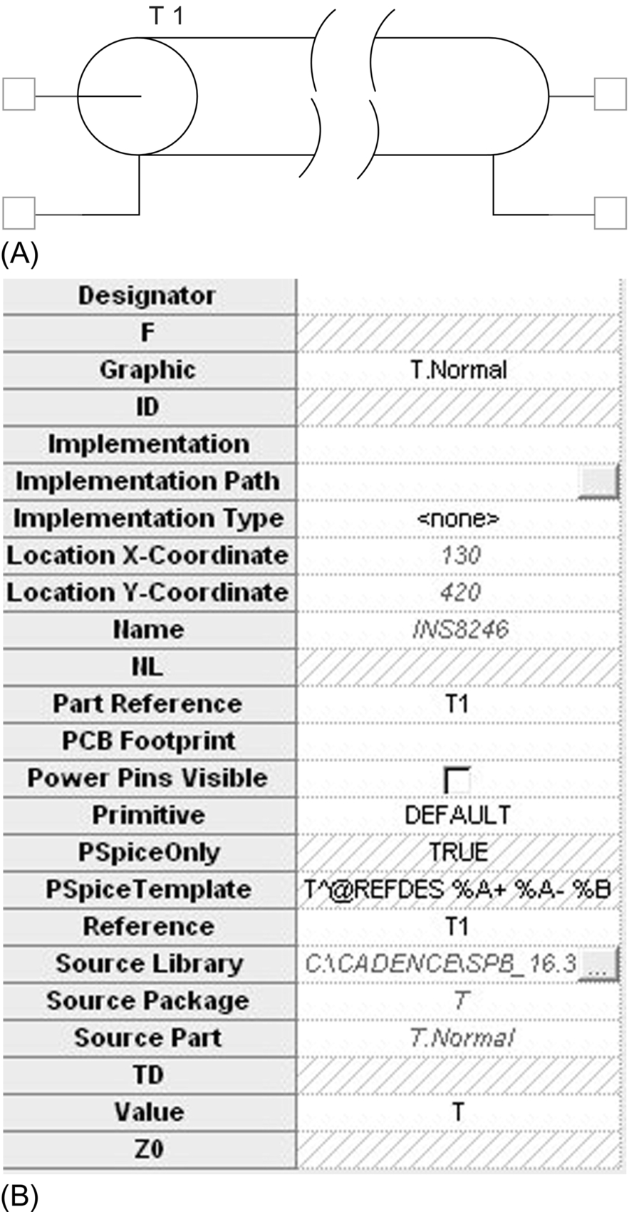
PSpice uses a T device from the analog library to model an ideal transmission line. Fig. 17.1A shows the Capture part for the T device and Fig. 17.1B the associated properties in the Property Editor.
So, for an ideal transmission line, if you do not know the delay time (TD) then you can enter values for NL and f and, as mentioned above, if you do not enter the frequency, then the default value of 0.25 is used, which represents the quarter wave frequency.
Initial conditions for voltage and current can be applied to the transmission line.
17.2 Lossy Transmission Lines
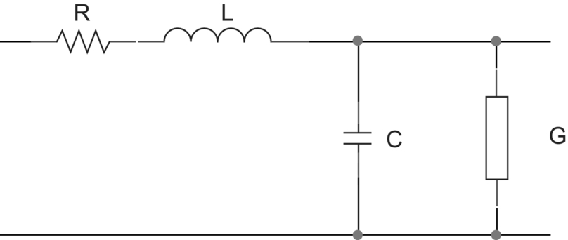
Transmission lines can be considered to consist of a number of identical sections known as RLCG lumped line segments, as shown in Fig. 17.2. The R represents the line resistance, L the line inductance, C the dielectric capacitance and G the dielectric conductance. For long transmission lines, one solution would be to use a number of lumped RLCG segments connected together. PSpice provides lumped line segments of up to 128 segments in the TLine library. However, lumping together large line segments can lead to long simulation times.
Simpler RC transmission line models are also available in the TLine library, as are over 40 coaxial cable models and twisted wire pair models.
An alternative approach for lossy transmission lines is to use a distributed model which relies on an impulse response convolution method to determine the transmission line response. Fig. 17.3 shows the TLOSSY PSpice device and the associated properties in the Property Editor.
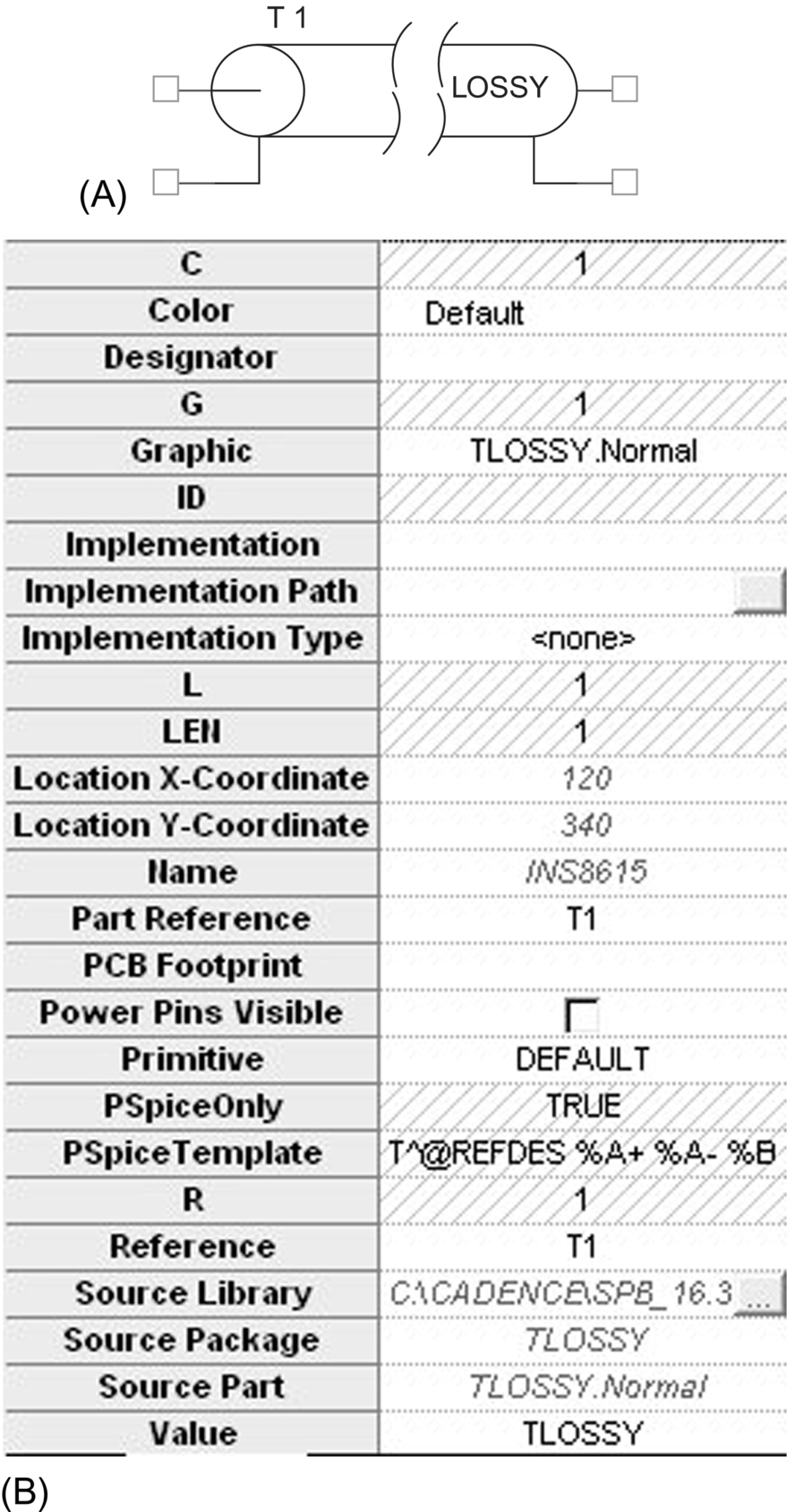
The length of the transmission line is represented by the LEN property and the R, L, C and G properties are specified as per unit length.
17.3 Exercises
The following exercises demonstrate the basic transmission line characteristics for different load terminations.
Exercise 1
Matched Load for RL
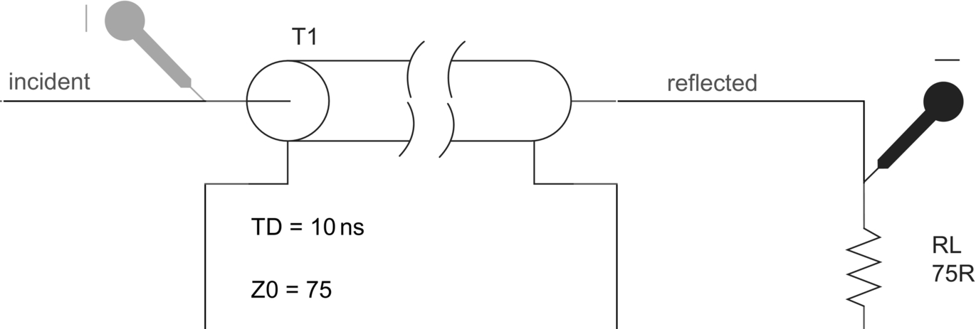
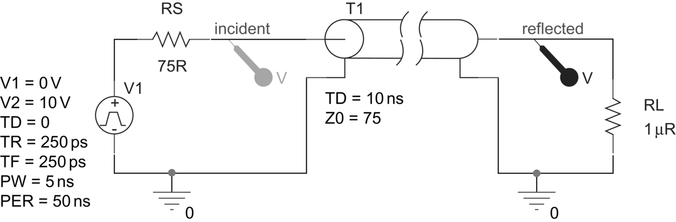
1. Draw the circuit in Fig. 17.4. The transmission device T is from the analog library and the voltage pulse is from the source library. When you place the load resistor, RL, on the schematic, by default, pin 1 is on the left-hand side. Rotate resistor RL three times such that pin 1 is at the top, which connects to T1. By convention, current flowing into pin 1 is defined as positive, such that a measured negative current at pin 1 represents a current flowing out of pin 1.
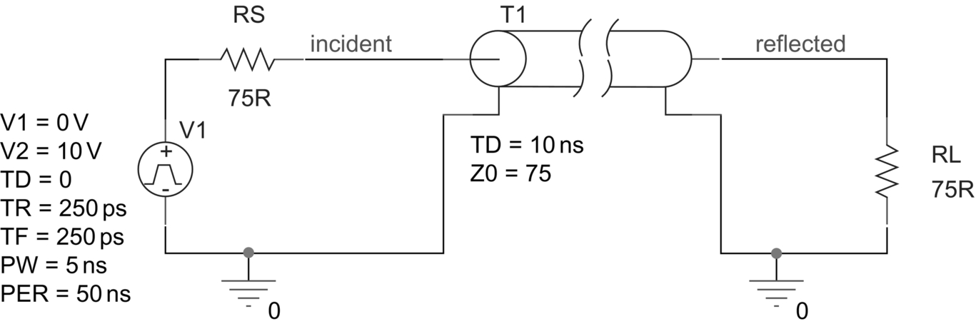
2. Double click on T1 to open the Property Editor and add and display the property values as shown in Fig. 17.5.
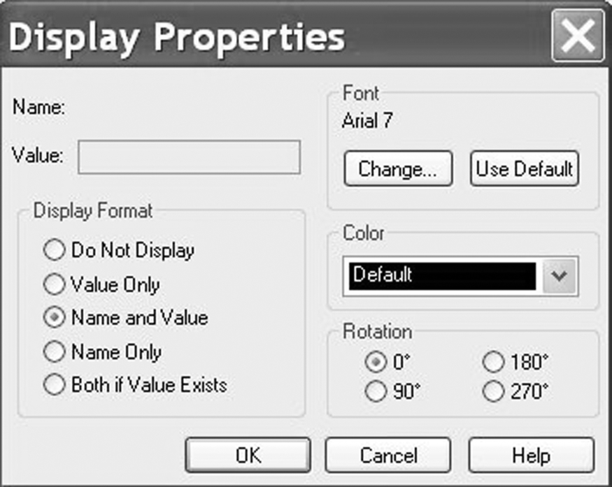
Highlight both TD and Z0 by holding down the control key, select Display and in the Display Properties window, select Display > Name and Value as shown in Fig. 17.6.

3. Create a transient analysis simulation profile with a Run to time of 50 ns and a Maximum step size of 100 ps (Fig. 17.7).

4. Add voltage markers on the incident and reflected nodes (Fig. 17.8) and run the simulation.

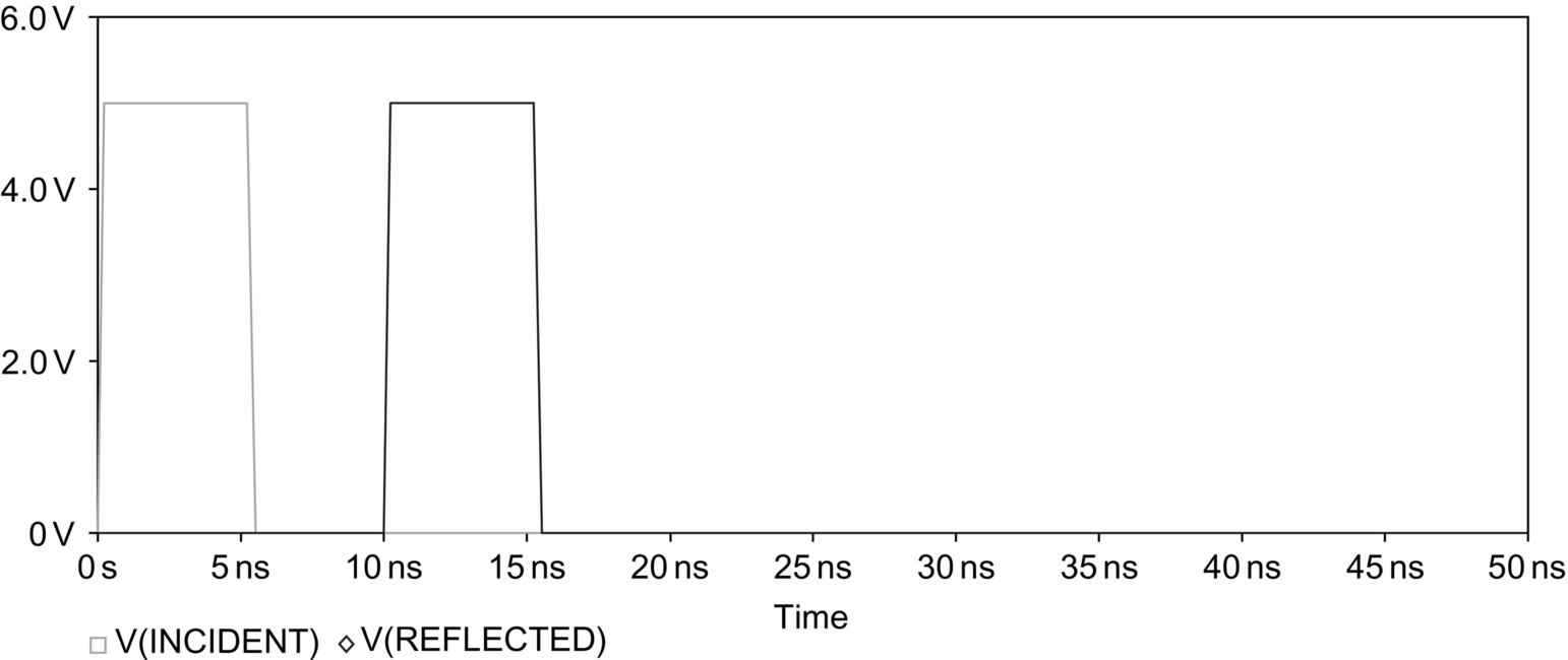
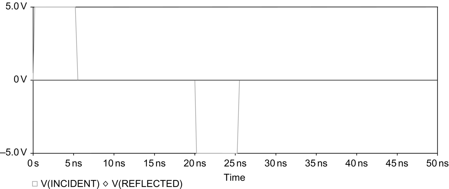
5. Fig. 17.9 shows the source pulse and the delayed load pulse after 10 ns. Initially, the source resistor and transmission line act as a potential divider, so the voltage amplitude divides down to 5 V.
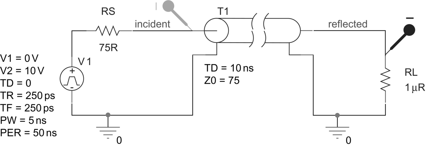
6. Delete the voltage markers in Capture and place current markers on the input pin (incident) to T1 and the top pin of the load resistor, RL (Fig. 17.10).
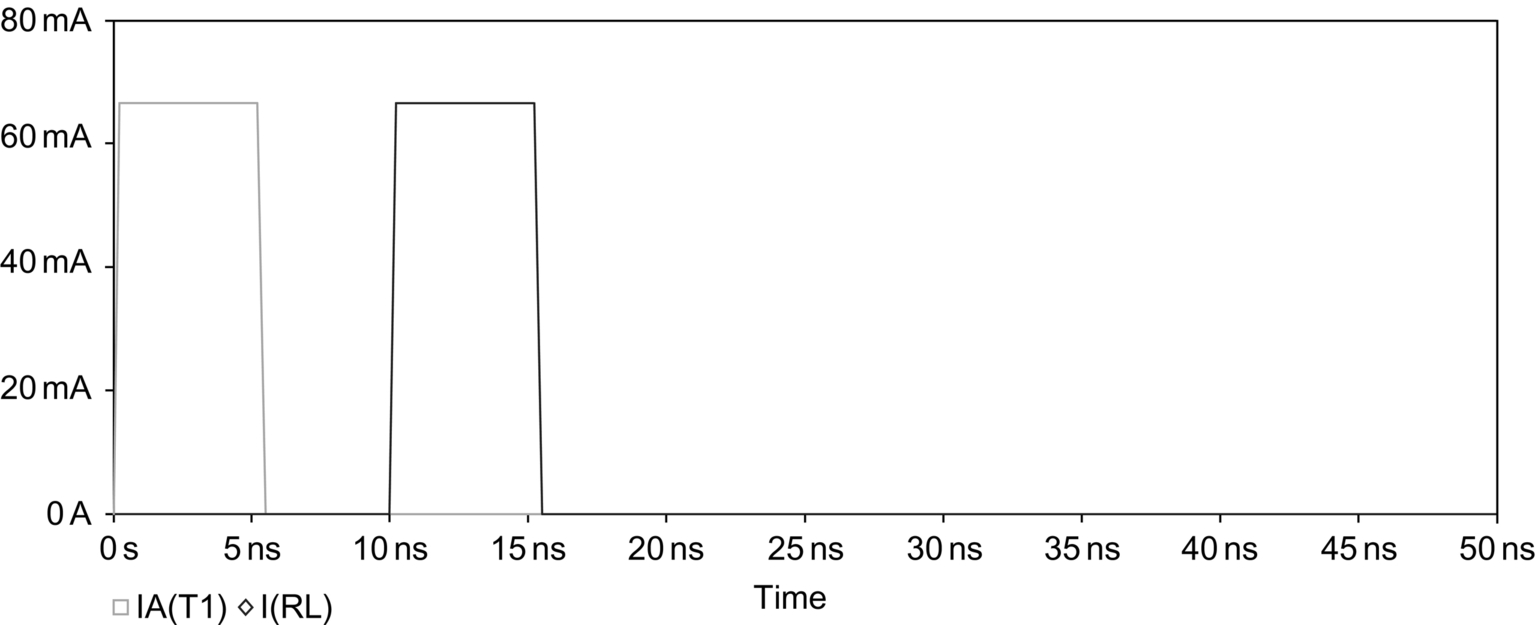
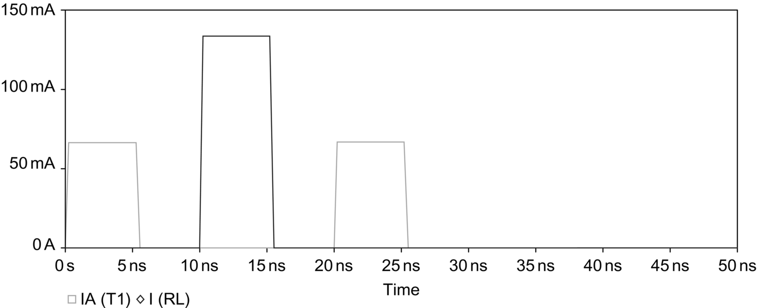
There is no need to rerun the simulation as the waveform display in Probe will automatically be updated. You should see that both currents have the same magnitude and are separated by the specified 10 ns delay (Fig. 17.11).
As the load impedance is equal to the impedance of the transmission line, the line is said to be matched. There are no voltage or reflections.
RL Replaced With a Short Circuit
7. Delete the current markers and replace the load resistance with a small value resistance of 1 μΩ to represent a short circuit. Place voltage markers on the incident node and the top of the short circuit resistor as shown in Fig. 17.12 and rerun the simulation.
You should see the transmission line response in Fig. 17.13. With a short circuit the load voltage will be 0 V and the incident voltage wave will be reflected but 180° out of phase with the incident wave.
8. In Capture, delete the voltage markers and place current markers on the input pin (incident) to T1 and the top pin of the RL resistor (Fig. 17.14).
There is no need to rerun the simulation as the waveform display in Probe will automatically be updated. You should see that the incident current wave is reflected with the same amplitude such that the reflected wave is double the magnitude of the incident current wave (Fig. 17.15).
RL Replaced With an Open Circuit
9. Delete the current markers and change the load resistance to a 1 TΩ resistor to represent an open circuit. Place voltage markers on the incident node and the top of the short circuit resistor (Fig. 17.16) and rerun the simulation.
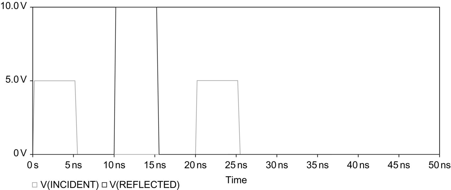
You should see the response shown in Fig. 17.17. The reflected voltage is equal to the source voltage, so the reflected voltage is double in magnitude to that transmitted.
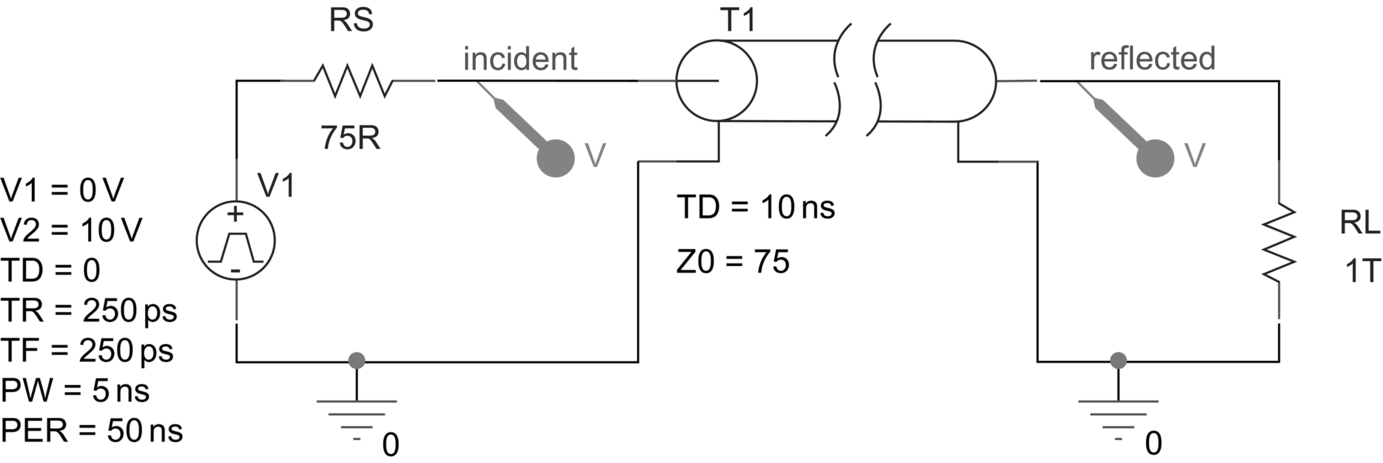
10. Delete the voltage markers in Capture and place current markers on the input pin (incident) to T1 and the top pin of resistor RL. There is no need to rerun the simulation as the waveform display in Probe will automatically be updated. As the output is an open circuit, no current will flow. The current at the open circuit is reflected back with the same magnitude but is 180° out of phase, as seen in Fig. 17.18.

Exercise 2
Standing Wave Ratio (SWR)
Fig. 17.19 shows a lossless transmission line with a short circuit. As shown in Fig. 17.13, the incident voltage is reflected with the same amplitude but 180° out of phase. The incident and reflected waves will sum together to produce a standing wave, otherwise known as a stationary wave, as will be demonstrated below.

SWR for Short Circuit
1. Delete the current markers and change the value of RL to 1 μR for a short circuit. Delete the voltage pulse, V1, and replace with a VAC source from the source library.
As mentioned previously, you cannot use TD and NL together, so you can either delete the TD property in the Property Editor or replace the transmission line with a new part.
2. Delete the transmission line T1.
3. Place a T part from the analog library.
4. We are going to vary the value of the transmission line property NL, so we need to parameterize the property value of NL in the Property Editor. Double click on the T part to open the Property Editor. Highlight the NL property value box which has shaded lines and enter {wavelength} (Fig. 17.20). As soon as you start typing, the shaded lines in the NL value box will disappear. The {} brackets represent a placeholder for a variable parameter. Do not close the Property Editor.

5. It is a good idea to display new properties. In the Property Editor, highlight the wavelength property and select Display (or rmb > Display) and select Name and Value as shown in Fig. 17.21. Do not close the Property Editor.

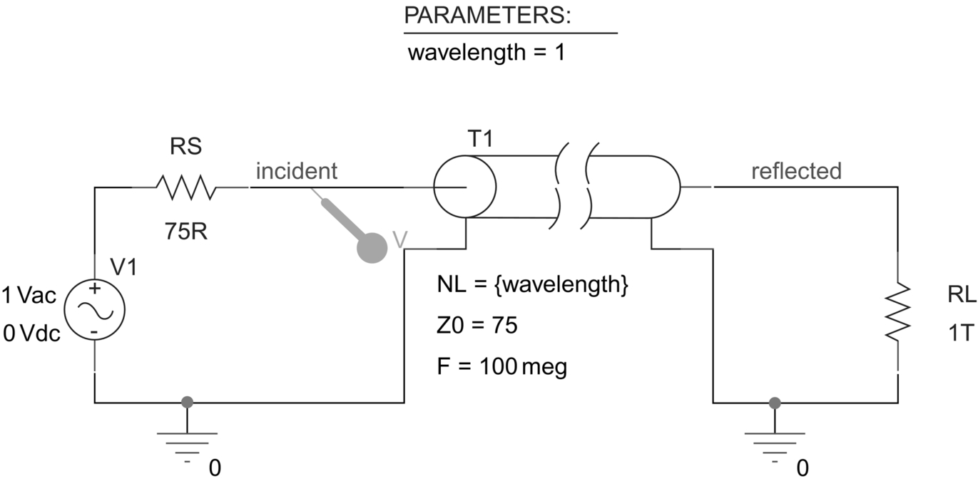
6. Set and display, as in Step 5, the name and property values for a frequency, F, of 100 megHz and a characteristic impedance, Z0, of 75R, as shown in the circuit diagram Fig. 17.19. Close the Property Editor.
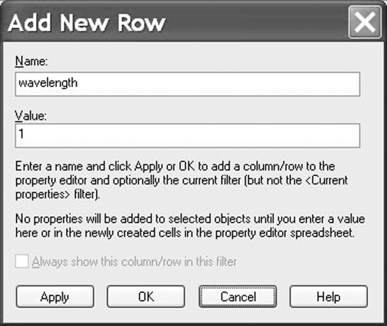
7. A default value for the wavelength parameter needs to be defined. Add a Param part from the special library and double click on the part to open up the Property Editor. Select New Row (or New Column) and enter the property Name as wavelength and property Value as 1 shown in Fig. 17.22.
8. Display the name and value of the wavelength property and close the Property Editor.
9. Your schematic should now appear as shown in Fig. 17.19.
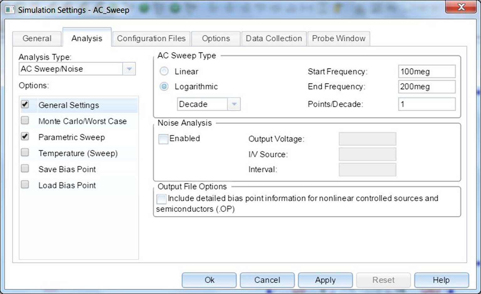
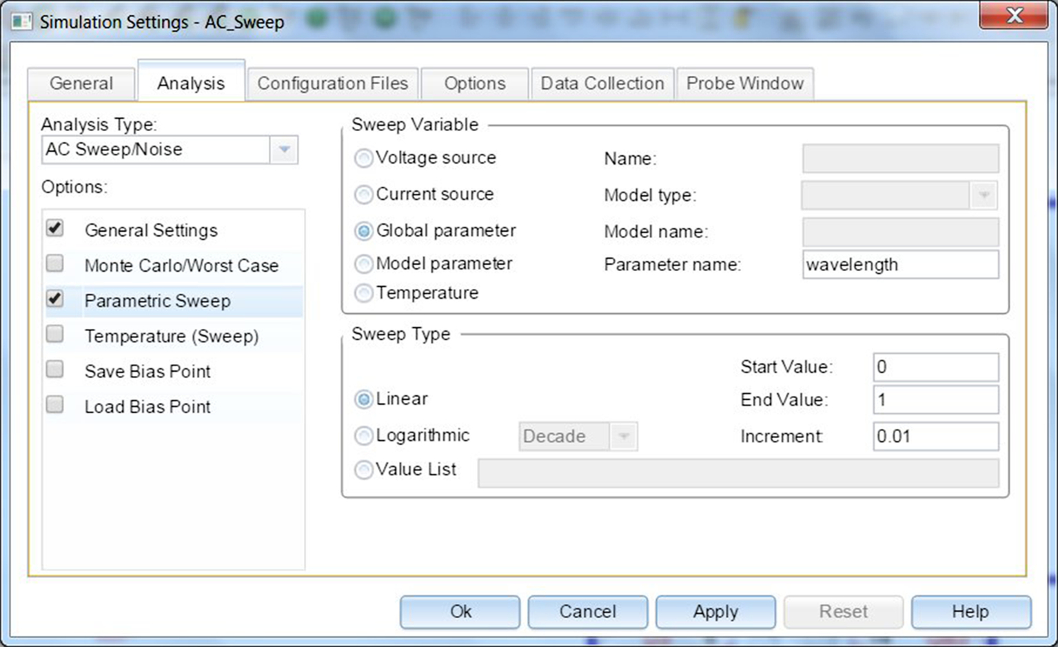
10. You will need to set up a Parametric simulation sweep together with an AC analysis. Create a new PSpice simulation profile, PSpice > New Simulation Profile, and select the analysis for AC Sweep/Noise from 100 to 200 megHz using a Linear sweep with the Total Points equal to 1 (Fig. 17.23). Click on Apply but do not exit the simulation profile.
In the Options box, select Parametric Sweep and set up a global parametric sweep of the wavelength property from 0 to 1 in steps of 0.01, as shown in Fig. 17.24. Click on OK.
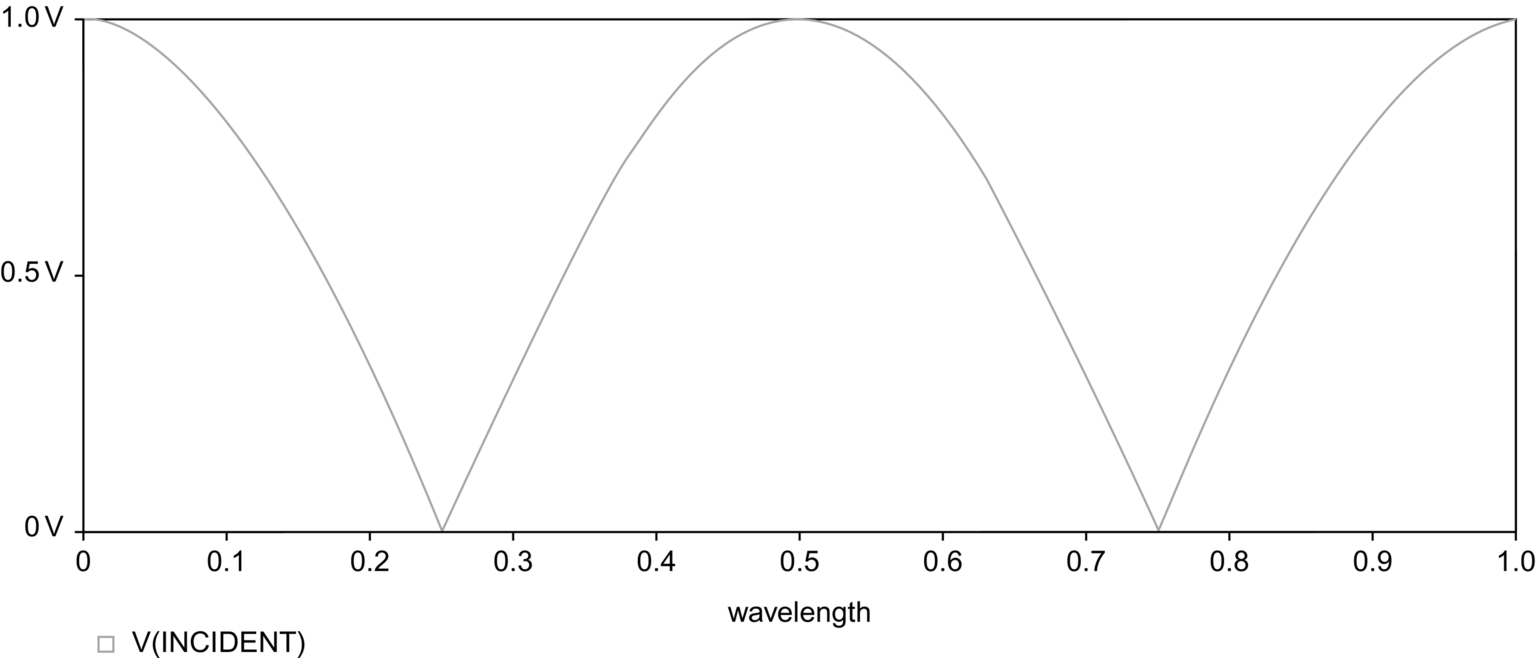
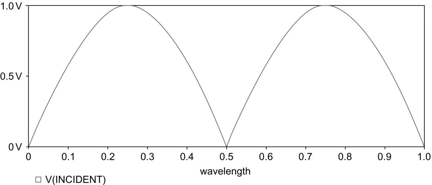
11. Place a voltage marker on the incident node and run the simulation. In the Available Sections window, make sure all sections are highlighted and click on OK. You should see the standing wave pattern in Fig. 17.25.
SWR for Open Circuit
For an open circuit, the voltage is reflected back with the same amplitude but is 180° out of phase.
12. Modify the value of the load resistor in Fig. 17.26 to 1T to represent an open circuit and simulate the circuit using the same simulation profile.
You should see the standing wave as shown in Fig. 17.27.