
Parametric Sweep
Abstract
A parametric sweep allows for a parameter to be swept through a range of values and can be performed when running a transient, AC or DC sweep analysis. Parameters that can be varied include a voltage or current source, temperature, a global parameter, or a model parameter. A global parameter can represent a mathematical expression as well as a variable, and is defined using the PARAM part from the Special library. To define the global variable, users have to add a new property to the PARAM part by editing its properties via the Property Editor. The PARAM part has a heading called PARAMETERS, and contains a list of defined variables and their default values. The global parameter variable name and default value must be added to the PARAM part as a new property in the Property Editor. The PARAM part is found in the special library and is placed anywhere in the schematic page. The Property Editor is a spreadsheet that displays all the properties attached to a part. When first selected, the Property Editor will open up in one of the two modes, displaying the properties in either rows or columns. The properties listed in the Property Editor have a name and a value. By default, new property names and values are not displayed on the part in the schematic diagram so they have to be made visible.
Keywords
Temperature; Parameter; Transient; Frequency; Amplifier; Circuit
A parametric sweep allows for a parameter to be swept through a range of values and can be performed when running a transient, AC or DC sweep analysis. Parameters that can be varied include a voltage or current source, temperature, a global parameter or a model parameter. A global parameter can represent a mathematical expression as well as a variable and is defined using the PARAM part from the Special library. To define the global variable, you have to add a new property to the PARAM part by editing its properties via the Property Editor. For example, in the resistor circuit shown in Fig. 5.1, the value of resistor R2 has been replaced with a variable called {rvariable}; you can name the variable anything you like. The braces otherwise known as curly brackets { } are required in PSpice to define global parameters.

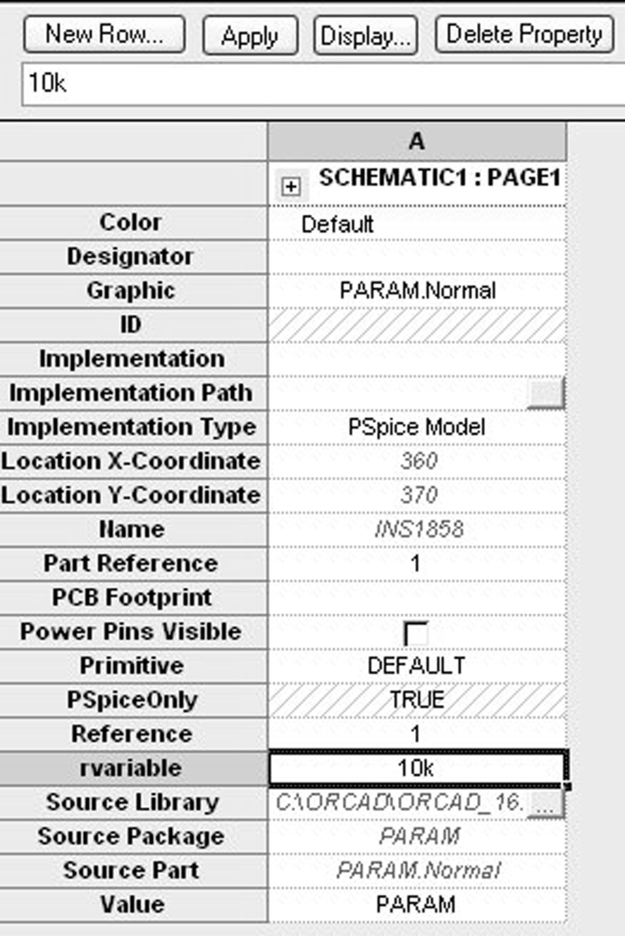
The PARAM part has a heading called PARAMETERS: and contains a list of defined variables and their default values. In this case, RL is defined to have a default value of 10 kΩ if no parametric sweep is performed.
5.1 Property Editor
As mentioned above, the global parameter variable name and default value must be added to the PARAM part as a new property in the Property Editor. The PARAM part is found in the special library and is placed anywhere in the schematic page. By double clicking on the PARAM part, the Property Editor (Fig. 5.2) will open.

The Property Editor is a spreadsheet that displays all the properties attached to a part. For example, a resistor will have defined properties such as a footprint, resistor value, power rating, tolerance, manufacturer's part number and PSpice model. Properties can be added to parts in the Property Editor and in the case of the PARAM part, we need to add a property to define the global variable that needs to be swept.
When first selected, the Property Editor will open up in one of two modes, displaying the properties in either rows (Fig. 5.3A) or columns (Fig. 5.3B).
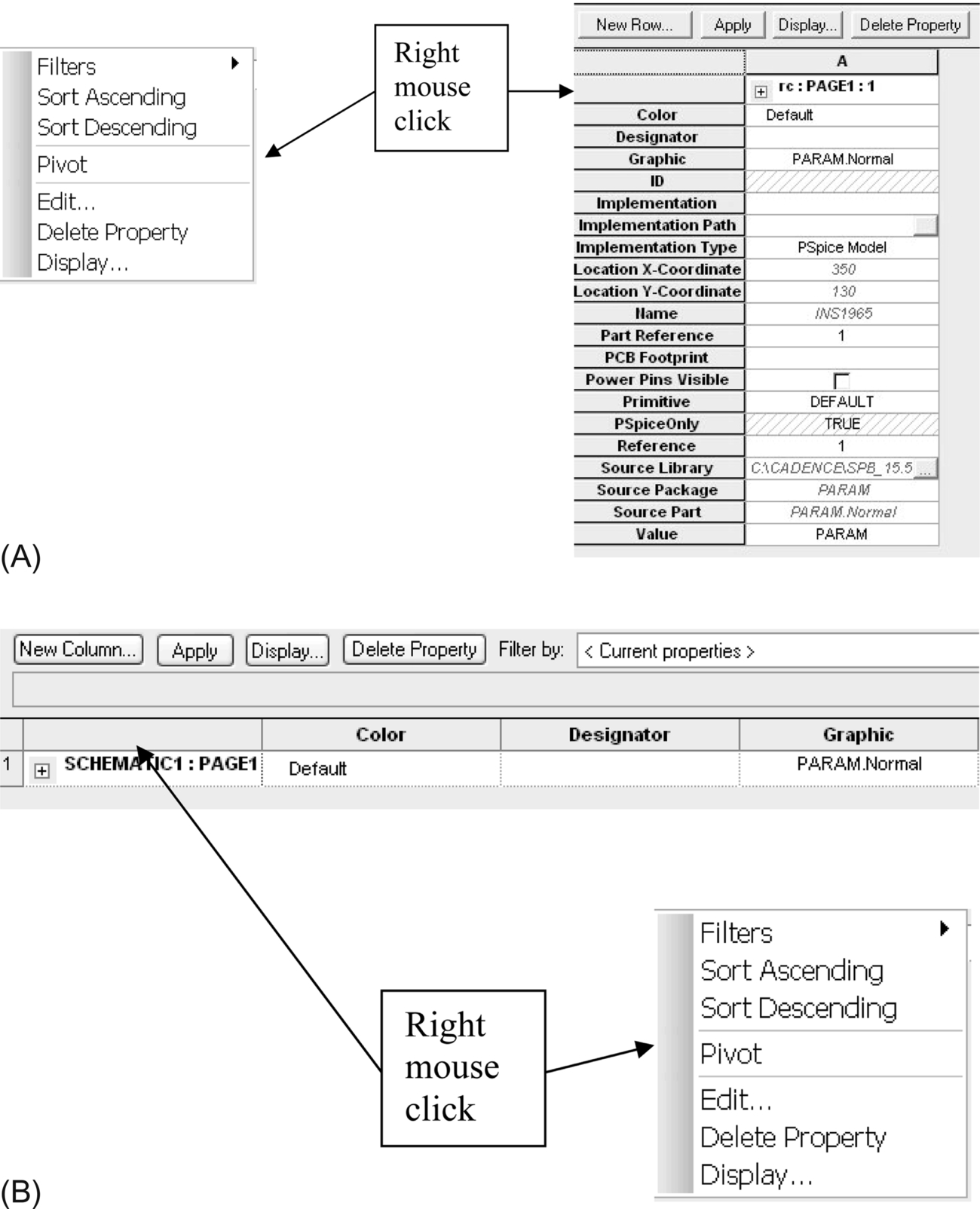
It is easier to view all the properties listed in rows, as shown in Fig. 5.3A. If the properties are displayed in columns (Fig. 5.3B), you will have to use the scrollbar at the bottom of the Property Editor to scroll along to view all the other properties. The viewed mode can be changed, for example, from columns to rows by placing the cursor in the blank cell to the left of the Color property (Fig. 5.3B) and when the cursor changes to an arrow, rmb > Pivot. The properties will now be displayed as rows.
To change the view from rows to columns, place the cursor in the blank cell above the Color property (Fig. 5.3A). When the cursor changes to an arrow, rmb > Pivot.
To add a property which allows a global parameter to be swept, select New Row as shown in Fig. 5.3A and the Add New Row dialog box will appear (Fig. 5.4). Add the Name of the variable and the default Value of the variable. Fig. 5.4 shows a parameter called rvariable being defined with a default value of 10k and Fig. 5.5 shows the new row added in the Property Editor.

The properties listed in the Property Editor have a name and a value. For example, a transistor may have a standard TO5 footprint. Footprint is the property name and its value is TO5. Another example is a resistor with a 1% tolerance. Tolerance is the property name and 1% is the value of the property. Table 5.1 gives some examples of property name and value.
By default, new property names and values are not displayed on the part in the schematic diagram so they have to be made visible. This is done by highlighting the property cell in the Property Editor and selecting Display (or rmb > Display). This will open up the Display Properties dialog box as shown in Fig. 5.6.
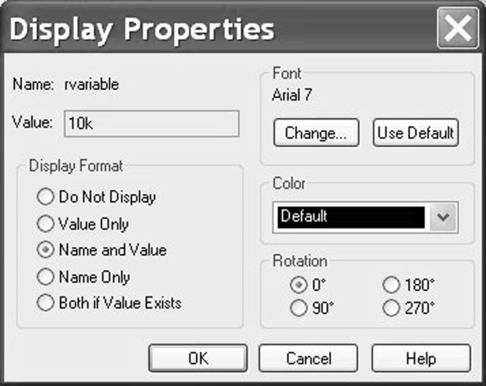
It is recommended for Global parameters that both property name and value are both displayed when added to the Param part, as seen in the resistor circuit in Fig. 5.1.
Note
The Property Editor is closed by clicking on the lower right hand cross of the property window. Be careful not to select the upper top cross as this will close Capture  .
.
5.2 Exercises
Exercise 1
When you connect audio equipment together, for example the output of a microphone to the input of an amplifier, it is recommended that the output impedance of the microphone should match the input impedance of the amplifier. This is also true for video and radio frequency (RF) equipment. What happens is that the maximum power transfer of a signal between a source impedance and a load impedance occurs when the impedances match and the maximum power transfer that can be achieved is 50% of the source signal.
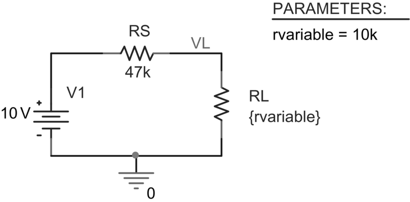
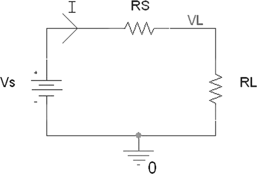
You will demonstrate simple resistance matching by plotting the load resistor power dissipation against load resistance for the circuit in Fig. 5.7.
1. Create a new PSpice project or use the resistor project from Chapter 1 as a starting point.
2. Place a VDC source from the source library and set its value to 10 V.
Place a resistor R from the analog library and name it RS and set its value to 47k. Place resistor RL and set its value to {rvariable}.
Connect a 0 V symbol from the capsym library (Place > Ground).
Name the net node connecting RS to RL as VL (Place Net > Alias) (Fig. 5.7).
3. Place a PARAM part from the special library anywhere on the schematic.
4. Double click on the Param part to open the Property Editor.
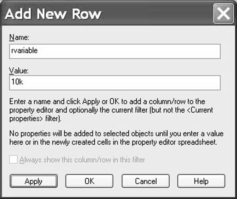
5. Depending on how the properties are displayed in the Property Editor (rows or columns), add a new property by either clicking on New Row… or New Column… Create a new property called rvariable with a value of 10k as shown in Fig. 5.8.
The circuit is now set up with a global parameter, rvariable, with a default value of 10 kΩ, which will be the resistor value used for simulation if no parametric sweep is performed. Click on OK but do not exit the Property Editor.
6. Highlight the new property rvariable and select Display. In the Display Properties window (Fig. 5.9) select Name and Value. Close the Property Editor.

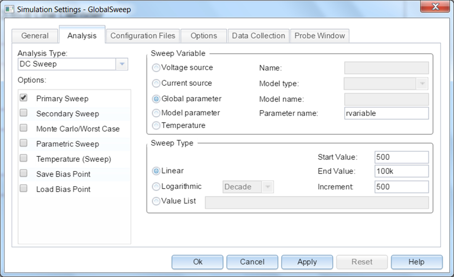
7. You will need to set up a DC sweep with a Global parameter named rvariable for a linear sweep from 500 Ω to 100 kΩ in steps of 500 Ω.
Create a new simulation profile, PSpice > New Simulation Profile, and call it anything you like, for example, global sweep.
Select Analysis type to DC Sweep and select the Sweep variable as a Global parameter with a Parameter name: rvariable. The Sweep type will be linear with a start value of 500 Ω, an end value of 100 kΩ and an increment value of 500 Ω (Fig. 5.10).
8. Place a power marker on the body of RL, i.e. in the middle of RL, by selecting PSpice > Markers > Power Dissipation, or select the icon  or
or 
Your circuit should look the same as that in Fig. 5.7.
9. Run the simulation (PSpice > Run)  .
.
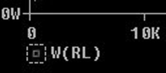
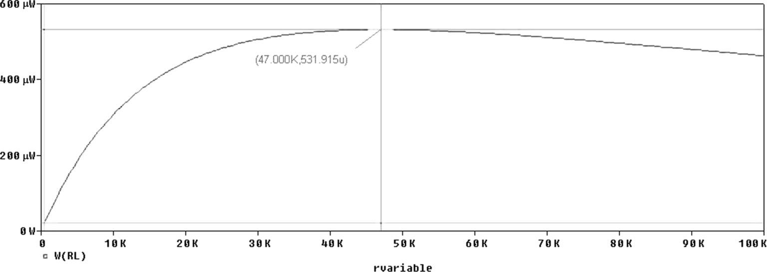
You should see the power dissipation curve in Fig. 5.11.
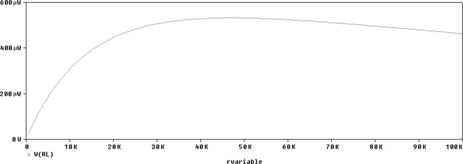
10. From the curve in Fig. 5.11 the cursors can be turned on to determine the value of load resistance for maximum load power (Figs. 5.12–5.14).
Display the cursor, Trace > Cursor > Display  or
or  .
.
In Probe, there are two cursors and they follow either the left mouse button(lmb) or the right mouse button (rmb). When you first select Cursor > Display, a dashed white box will appear around the symbol used for the trace name (Fig. 5.12).
The cursor will then follow the left mouse with the left mouse button held down. The cursor box will then appear and give a coordinate reading of the cursor. In release 16.2 and previous versions (Fig. 5.13a), A1 is the left mouse cursor with the first value the x-coordinate and the second value the y-coordinate. A2 is the second cursor, which follows the right mouse button. From release 16.3, the cursors are labeled as shown in Fig. 5.13b, where you can also add multiple cursor measurements from other traces and plots.
11. Place the cursor on the maximum point of the curve and read off the value for the load resistor.
Alternatively, there are predefined cursor functions (Fig. 5.14) which can be used to find the points on the curve such as maximum or minimum values. These can be accessed from Trace > Cursor or you can select the readily available icons on the top toolbar.
The function of each icon is shown by moving the cursor over the icons.
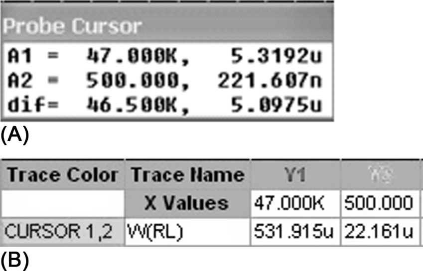
12. Select the Cursor Max function and you will see the cursor move to the maximum value on the curve. The cursor box then displays the maximum value as 47k, which is the load resistor value for maximum power transfer (Fig. 5.15).
13. With the cursor placed at the maximum value, select Plot > Label > Mark or click on the icon  or
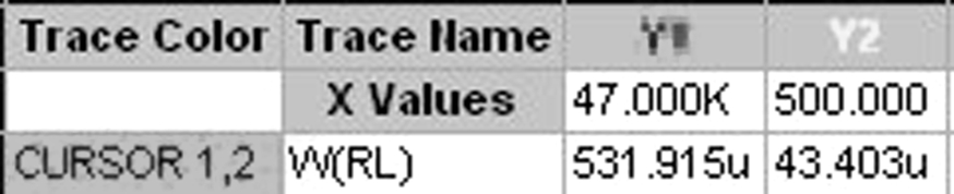
or  . The coordinates of the maximum point on the curve (47k, 531.915W) will now be marked and displayed (Fig. 5.16).
Theory
In Fig. 5.17, the current in the circuit is given by:
The power dissipated in the load resistor is given by:
Substitute for I from Eq. (5.1) into Eq. (5.2):
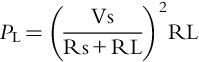
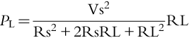
Dividing by RL:

For maximum power in Eq. (5.5), the denominator must be a minimum. Rather than differentiating the whole equation, differentiating the denominator will give the same result.
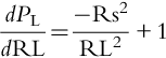
For a turning point,

Therefore,
It can be shown by differentiating Eq. (5.6) again, that the denominator is a minimum at the turning point and so when Rs = RL, the power is a maximum value.
Exercise 2
Notch Filter
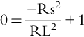
You will globally sweep the resistor values in the notch filter circuit from Chapter 4 on AC analysis to see what effect this has on the circuit response. In the circuit shown in Fig. 5.18, the four resistor values have been replaced by the global parameter {Rvalue}, which has been defined by the Param symbol to have a default value of 27k if no parametric sweep is performed.
1. Place a Param part from the special library. Double click on the Param part and define the global variable as Rvalue with a default value of 27k. Display both the property name and value for Rvalue. The steps are the same as in Exercise 1.
2. Create a PSpice simulation profile for an AC sweep with the same settings for the passive notch filter in Exercise 1, performing a logarithmic sweep from 10 to 10 kHz with 100 Points/Decade (Fig. 5.19). Click on Apply but do exit.
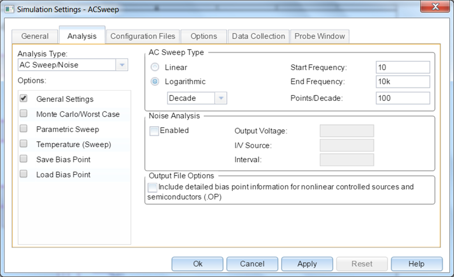
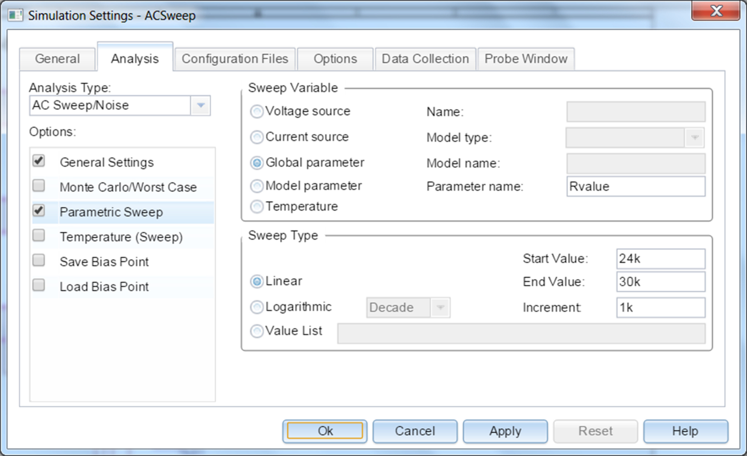
3. Select the Parametric Sweep in the Options box and set up a Global parametric linear sweep for the Rvalue variable starting at 24 to 30 kΩ in steps of 1 kΩ, which will perform a total of seven AC sweeps (Fig. 5.20). Click on OK.
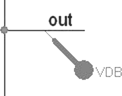
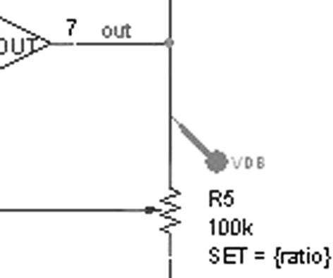
4. Place a Vdb marker on the output node, “out”. PSpice > Markers > Advanced > dB Magnitude of Voltage.
 .
.The notch filter response is shown in Fig. 5.21. Here you can see that the notch frequency changes with a change in resistance Rvalue. However, the attenuation depth of the notch, also known as the Q of the filter, also changes with frequency.

Exercise 3
Active Notch Filter
Fig. 5.22 shows an active notch filter built upon the previous twin T notch filter. The notch frequency is set as before by the resistor and capacitors in the passive network but the potentiometer R5 is used to set the Q (the sharpness of the attenuation) of the notch, which is not dependent on frequency.
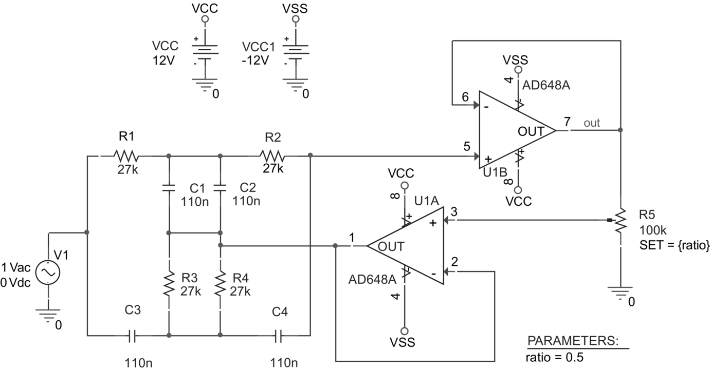
The potentiometer, R5, has a SET parameter which effectively sets up the ratio between the two resistances on either side of the potentiometer wiper (pin 2). For example, if the ratio is set to 0.4, the resistance between pins 1 and 2 takes on a value of 0.4 × 100 k = 40 k and the resistance between pins 2 and 3 takes on a value of (1 − 0.4) × 100 k = 60 k. So by varying the SET parameter between 0 and 1.0, the pot is effectively being turned through its complete resistance range.
Now, in order to automatically sweep the SET parameter through its range of 0 to 1.0, a global parameter, ratio, has been set up which has a default value of 0.5 corresponding to the midrange of the potentiometer (50 kΩ).
In order to draw the circuit of the active notch filter, the operational amplifiers (opamps) AD648A need to be found. Any opamps could be used, but this is a good exercise in how to search for specific parts.
1. In the Place Part menu there is a Search for Part function which can help to locate the opamp library as shown in Fig. 5.23.
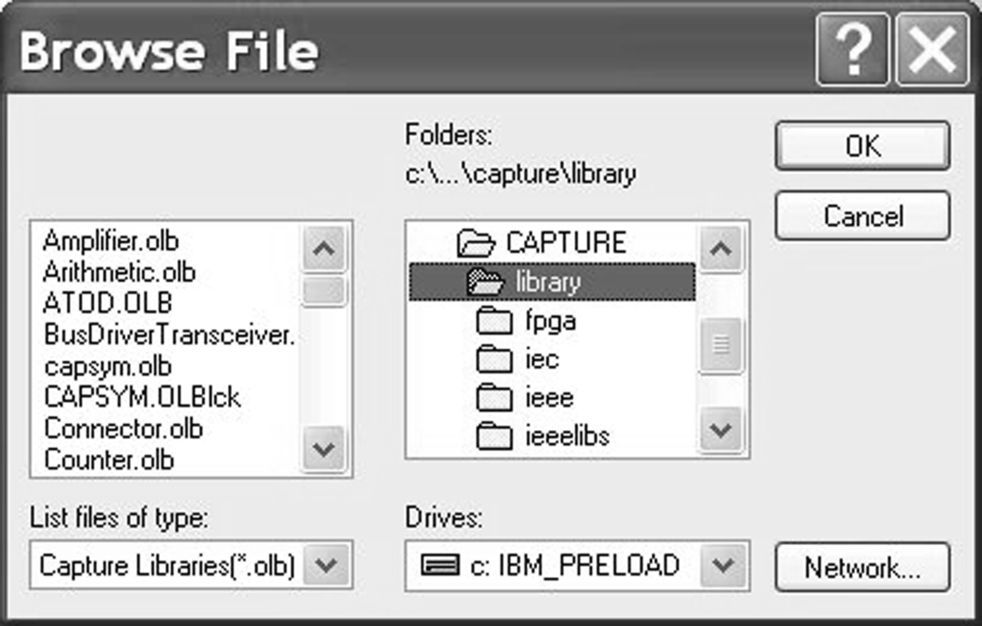
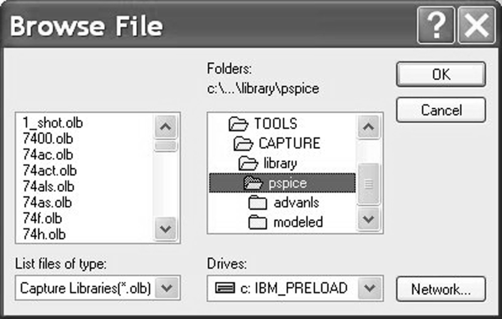
To change the search path, click on the Browse icon  to the right of the Search Path box, which will open the Browse File window (Fig. 5.24) showing the [install path] > capture > library folder selected on the right-hand side and the list of libraries in that folder shown on the left.
In the Folder section, scroll down and double click on the pspice folder as shown in Fig. 5.25. On the left-hand side, you will see a list of the available PSpice libraries. Click on OK.

2. Different manufacturers append their own specific numbers and letters to standard part numbers. For example, if you are searching for the BC337 transistor and type in BC337 in the Search For box, you will only see one result. However, if you type in a wildcard (⁎) after the transistor number, BC337 ∗, you will see more results because the wildcard effectively ignores the manufacturer's extra characters after the transistor number when doing a search.
In the Search for Part enter the opamp number, AD648 ∗, and either press return or click on the Part Search icon  .
.
There should only be one instance of the AD648A from the opamp library, as shown in Fig. 5.26. Double click on the AD648A and you will see the opamp library added to the list of libraries and a Capture graphical representation of the opamp.
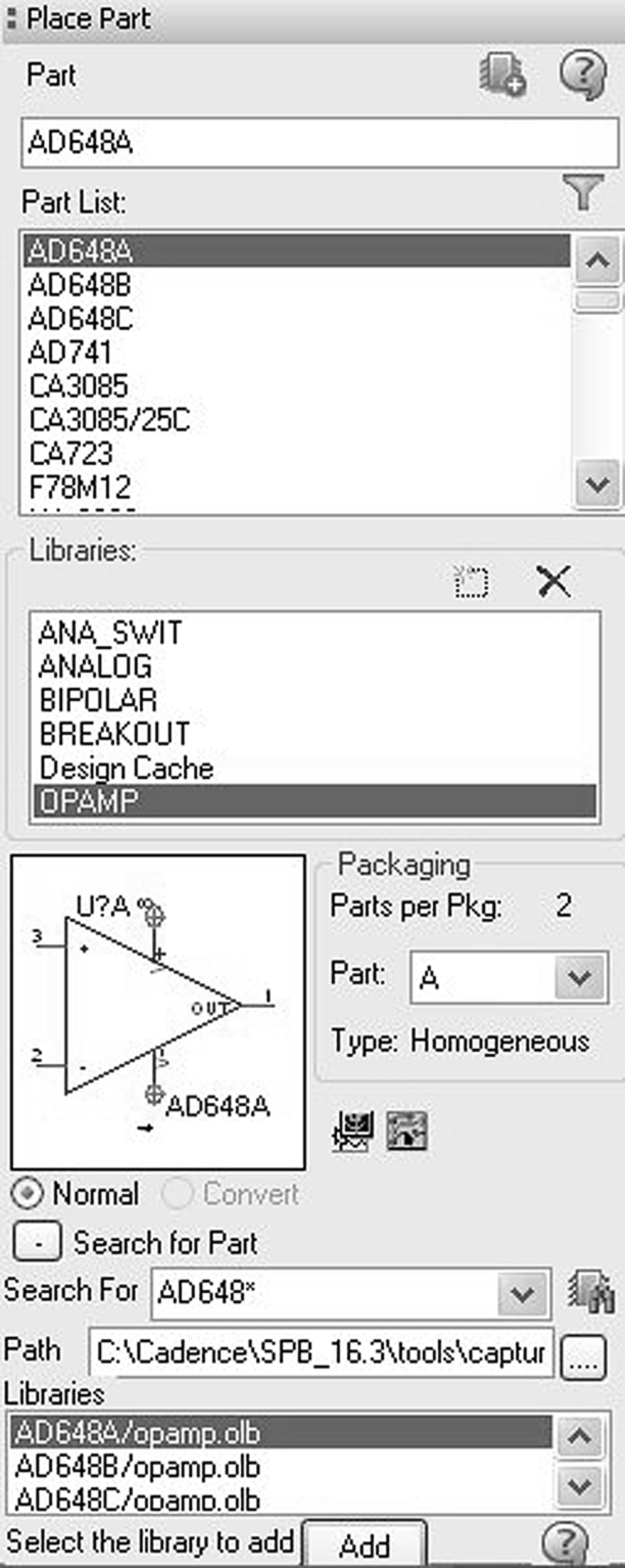
In the Place Part menu alongside the graphical representation of the opamp, there is a Packaging section which shows that there are two Parts per package. As this is a dual opamp, there are two available sections, A and B. Fig. 5.26 shows Part A selected, while Fig. 5.27 shows Part B selected. Note the different pin numbers and different reference designators, U?A and U?B. Type: Homogeneous indicates that both sections in a part are the same, in contrast to, for example, a relay and coil, where both sections are different and are classed as heterogeneous.
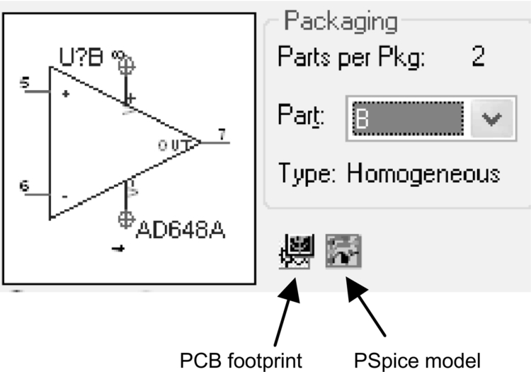
The two icons shown in Fig. 5.27 indicate that the AD648A has PCB footprint and a PSpice model attached and is therefore ready for simulation. It is important that the PSpice icon is displayed when selecting parts for simulation.
3. Place the A part of the opamp in the circuit. Highlight the opamp and rmb > Mirror Vertically or press V. The Mirror and Rotate operations can be used even if the opamp is connected in the circuit. You do not have to delete any wires.
4. Select the B part of the opamp and place it in the circuit.
5. With all the libraries selected (left mouse click at the top of library list and drag mouse pointer down to bottom of library list), type pot, in the Part box. The pot is found in the breakout library. Place the pot part and change its value to 100k. Double click on the SET property and change the default value of 0.5 to {ratio}. Do not forget the brackets.
6. We need to define ratio as a global parameter with a default value of 0.5. Place a Param part from the special library in the circuit.
7. Double click on the param part and enter a new row (or new column). Create a new property called ratio with a value of 0.5 and display the property name and value. The steps are the same as in Exercise 1.
8. Select Place > Power and scroll down to the VCC_CIRCLE symbol and in the Name: box, change the name to VCC and click on OK. Repeat for the VSS symbol.
9. Place and connect the remaining components as shown in Fig. 5.22.
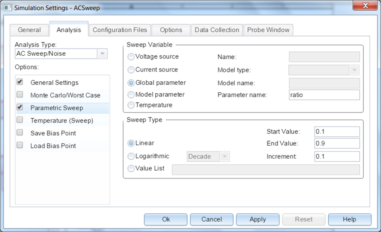
10. The parametric sweep is run in conjunction with an AC analysis. In this example we are going to run a parametric sweep on the potentiometer ratio from 0.1 to 0.9 in steps of 0.1. The first thing to do is to set up the same AC analysis as before with the passive notch filter, sweeping the frequency logarithmically from 10 to 10 kHz with 100 points/decade (Fig. 5.28). Click on apply but do not exit.

11. Select the Parametric Sweep in the Options box. The Sweep variable is a Global parameter and the Parameter name is ratio. The Sweep type is linear, the Start value 0.1, the End value 0.9 and the Increment 0.1 (Fig. 5.29). Click on OK.
12. Place a Vdb marker on the output node “out”. PSpice > Markers > Advanced > dB Magnitude of Voltage.
13. Run the simulation  .
.
Fig. 5.30 shows that by varying R5, the Q of the circuit (the sharpness of the notch) can be varied without a change in the notch frequency.
