Analog Behaviorial Models
Abstract
Analog behaviorial models (ABM) devices are extended versions of the traditional Spice Voltage Controlled sources, the E device which is a voltage controlled voltage source and the G device, a voltage controlled current source. They provide transfer functions, mathematical expressions, or look up tables to describe the behavior of an electronic device or circuit. ABM's can provide a systems approach to designing electronic circuits. The electronic system is represented by a block diagram with each block represented by an ABM device which will reduce the total simulation time. If the system meets the required specifications, then each block can be successively replaced by its final electronic circuit. Alternatively, working electronic circuits can be replaced by an equivalent ABM block.
Keywords
Simulation time; Filter; ABM; Current; Delay functions; Comparators; Voltage sources
Analog behaviorial models (ABM) devices are extended versions of the traditional Spice Voltage Controlled sources, the E device which is a voltage controlled voltage source (VCVS) and the G device, a Voltage Controlled Current Source (VCCS). They provide transfer functions, mathematical expressions, or look up tables to describe the behavior of an electronic device or circuit. ABM's can provide a systems approach to designing electronic circuits. The electronic system is represented by a block diagram with each block represented by an ABM device which will reduce the total simulation time. If the system meets the required specifications, then each block can be successively replaced by its final electronic circuit. Alternatively, working electronic circuits can be replaced by an equivalent ABM block.
There are two types of ABM devices, PSpice equivalent parts which have a differential input and double-ended output and control system parts which have a single input and output pin. The standard E, F, G, and H devices can be found in the analog library, whereas the ABM devices can be found in the ABM library.
13.1 ABM Devices
The extended sources provide five additional functions which are defined as:
| Value | Mathematical expression |
| Table | Look up table |
| Freq | Frequency response |
| Chebyshev | Filter characteristics |
| Laplace | Laplace transform |
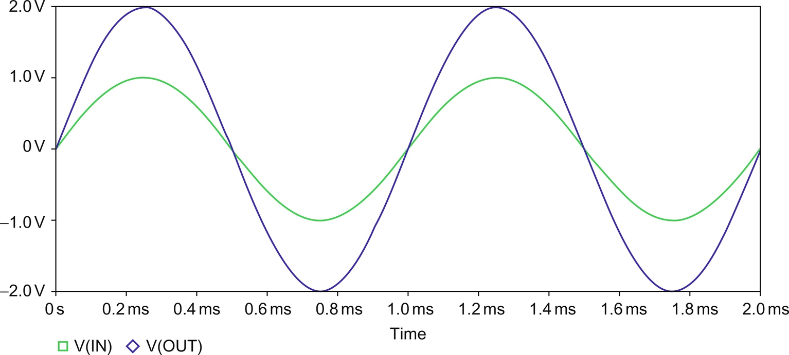
Fig. 13.1 shows a typical use of an ABM EValue device to implement a voltage doubler. The ABM has a differential input (IN +, IN −) and a double-ended output (OUT +, OUT −). When you first place the ABM, the default expression is given by

which calculates the difference between the voltages on the input pins IN + and IN −. In order to multiply by a factor of 2, the expression is first enclosed in curly brackets (braces).
Fig. 13.2 shows the output voltage when a 1 V sinewave is applied to the input pins.
Other mathematical functions that can be applied to ABM expressions are shown in Table 13.1.
Table 13.1
Mathematical functions
| Function | Expression |
| ABS | Absolute value |
| SQRT | Square root √ x |
| PWR | | x |exp |
| PWRS | xexp |
| LOG | Log base e ln(x) |
| LOG10 | Log base 10 log10(x) |
| EXP | ex |
| SIN | sin |
| COS | cos |
| TAN | tan |
| ATAN | tan− 1 |
| ARCTAN | tan− 1 |
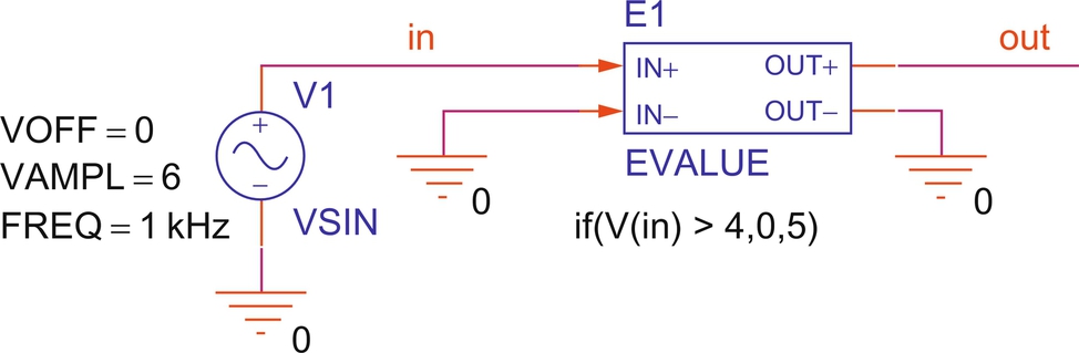
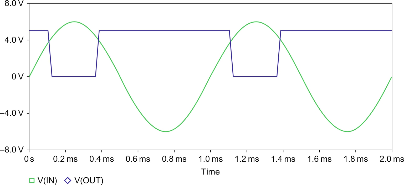
Conditional statements can also be applied to ABM parts. For example, in Fig. 13.3, if the input voltage is greater than 4 V, then output 0 V else output 5 V. This effectively is a comparator. The resulting waveform is shown in Fig. 13.4.
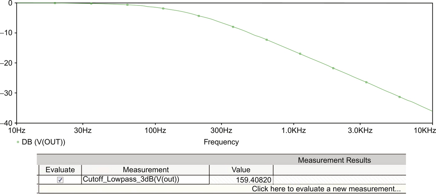
The first-order 159 Hz low pass filter in Fig. 13.5 can be defined by the transfer function:


where the cut off frequency is given by

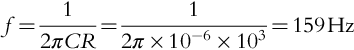
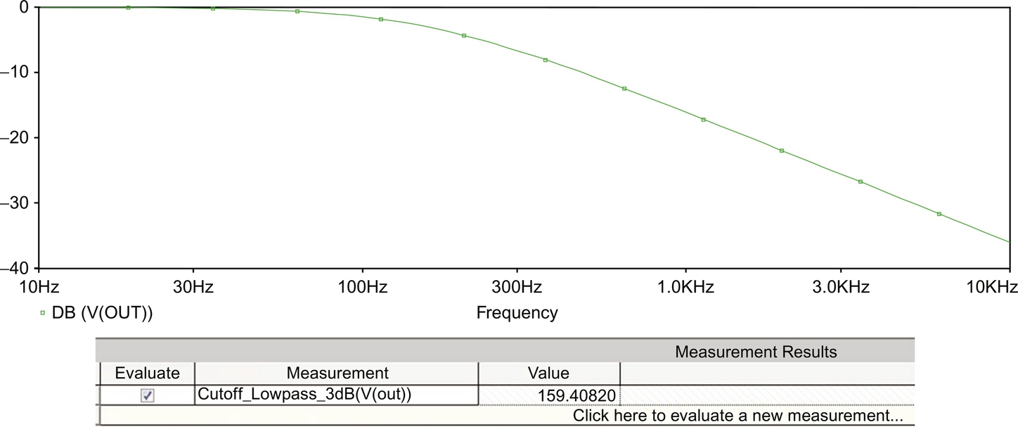
Fig. 13.6 shows the frequency response of the filter.
Laplace ABM's can be used to implement filter circuits where the transfer function is transformed to the s domain where s = jω and ω = 2πf so the transfer function for the low pass filter is defined in the s domain by
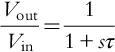
where
The filter circuit is redrawn in Fig. 13.7 with the transfer function given as:
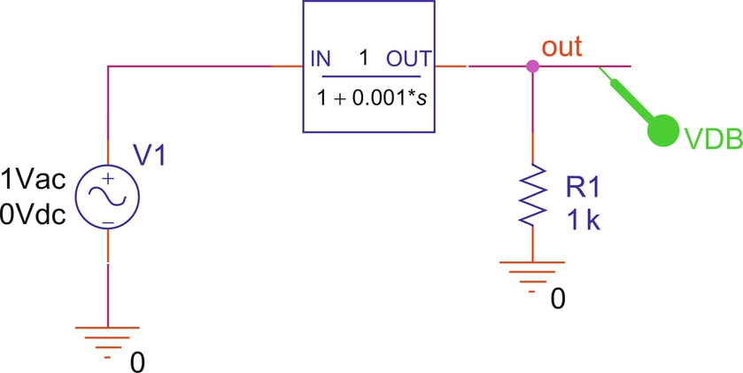

Fig. 13.8 shows the low pass frequency response for the filter.
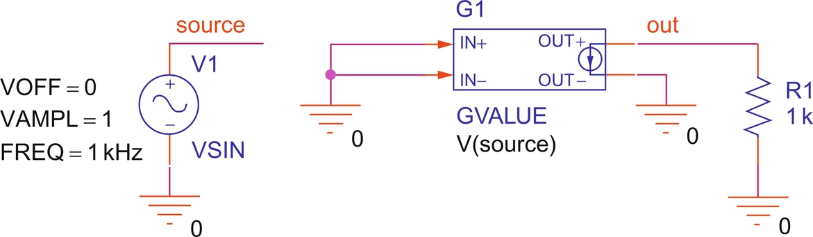
In the circuit of Fig. 13.9, both inputs are grounded but the ABM expression is referencing a net name called “source.” This is useful to reduce the wiring complexity of a circuit especially if there are multiple ABM's being driven by a single source. Note that since a GValue ABM part is being used, the output is a current and therefore cannot be left unconnected. Hence the output resistor provides a DC path to 0 V.
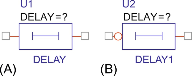
In version 17.2, two new behavioral delay functions have been introduced, DelayT() and DelayT1(). Both these functions have improved simulation times and more efficient handling of convergence issues compared to the standard delay functions such as TLINE. DelayT() requires two parameters, delay time and max delay, whereas DelayT1() only requires the delay value and also inverts the input signal. The delay functions are shown in Fig. 13.10 and can be found in the function.olb library in the advanced analysis folder.
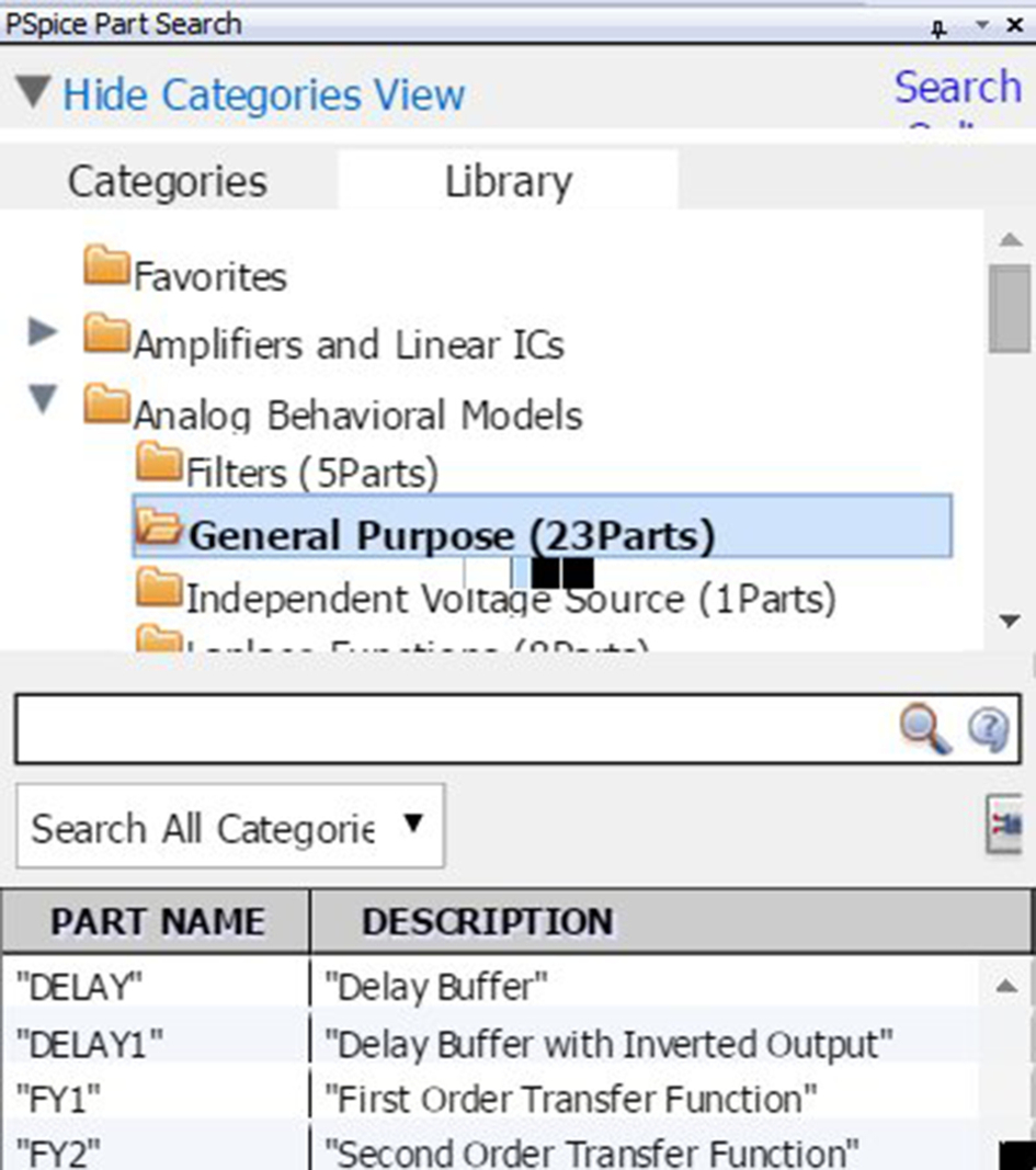
In later software versions you can search for the delay functions using:
Place > PSpice Component > Search
Then under Categories, select Analog Behavioral Models > General Purpose as shown in Fig. 13.11.
13.2 Exercises
Exercise 1
In Fig. 13.12, an EFreq ABM part is being used to model a bandpass filter using a table of parameters defining frequency, magnitude, and phase.
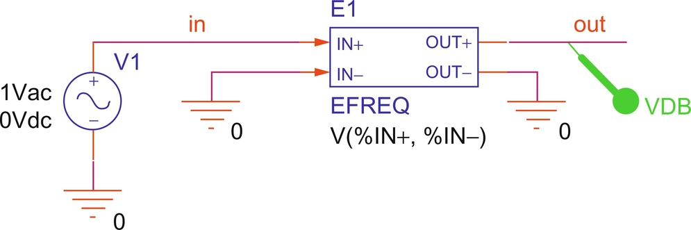
1. Draw the circuit in Fig. 3.12 using an EFreq part from the ABM library. The VAC source (V1) is from the source library.
2. Double click on EFreq to open the Property Editor and scroll to the Table property and enter:
(0.1,−40,170)(1 k,−40,160)(2 k,−20,140)(3 k,−0,100)(6 k,−0,−100)(10 k,−20,−140)(20 k,−40,−160)(30 k,−40,−170).
3. Set up a simulation profile for an AC Sweep from 1 to 100 kHz. Place a VdB voltage marker. PSpice > Markers > Advanced > dB Magnitude of Voltage.
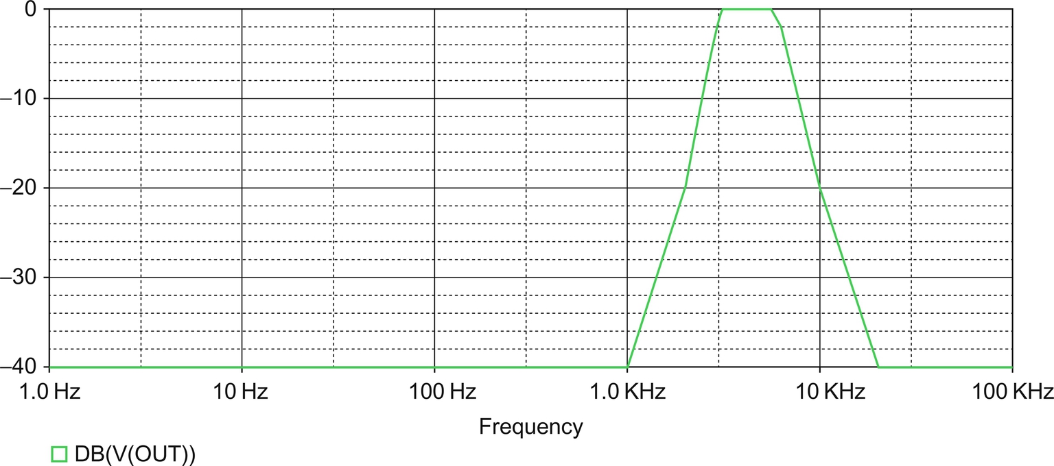
4. Run the simulation. You should see the bandpass response as shown in Fig. 13.13.
Exercise 2
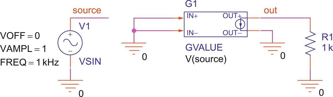
Use a GValue ABM to model to reference a net name and output a current.
1. Draw the ABM rectifier as shown in Fig. 13.14. The net name source is referenced inside the ABM expression brackets.
2. Set up a simulation profile for a transient sweep with a run to time of 4 ms.
3. Run the simulation.
4. Investigate the use of the EFREQ ABM device in modeling the 1500 Hz bandpass filter in Chapter 10.
Exercise 3
1. Draw the circuit in Fig. 13.15 using the Delay part. Either, Place > PSpice Component > Search > Analog Behavioral Models > General Purpose (23Parts) and select Delay or alternatively, use Place > Part and Add Library > advanls > function and select the Delay part.

2. Click on DELAY =? and add a delay value of 2 ms.
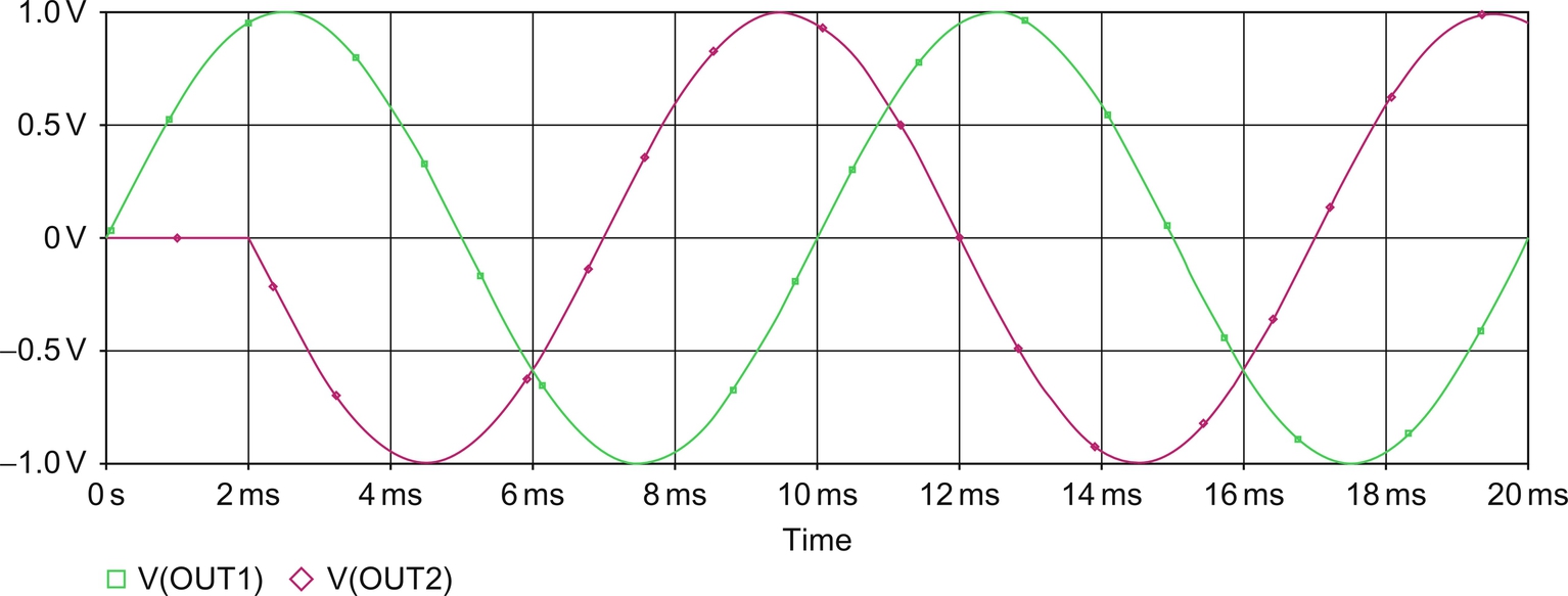
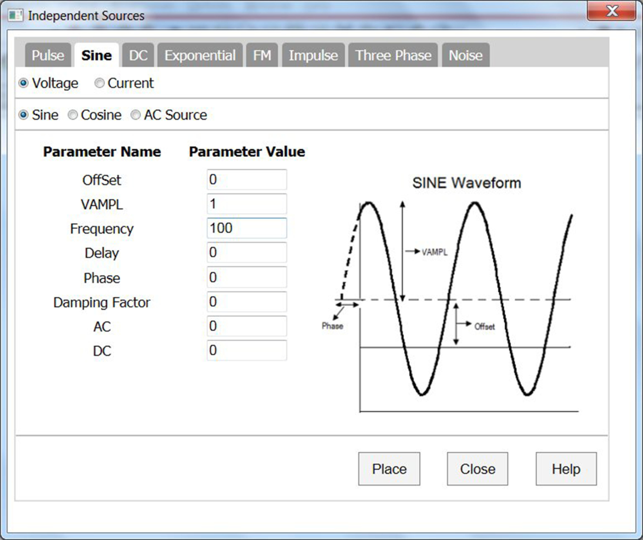
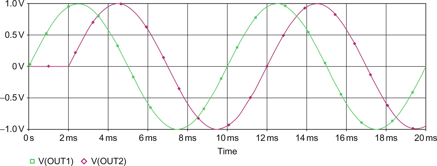
3. Place a 100 Hz, 1 V sinusoidal source from the source library. For later software versions, press shift-R to open the Independent Sources window as shown in Fig. 13.16.
4. Name the output signals as out1 and out2 and add voltage probes as shown and set up a transient analysis for a Run-To Time of 20 ms.
5. Run the simulation. Note that out2 has been delayed by 2 ms, see Fig. 13.17.
6. Replace the Delay part with a DelayT1 part and add a delay of 2 ms.
7. Run the simulation. Note that out2 has been inverted and delayed by 2 ms, see Fig. 13.18.