Mixed Simulation
Abstract
PSpice uses the same simulation engine for analog and digital circuits. The simulation results in Probe share the same time axis, but are split into separate analog and digital plot windows. Analog and digital components in a circuit are connected together at nodes. In PSpice there are three types of connecting nodes: analog (where all connected parts are analog), digital (where all connected parts are digital), and interface (where there is a mixture of analog and digital parts). Interface nodes are automatically separated into one analog node and one or more digital nodes by inserting analog and digital interface subcircuits, which are either analog to digital (A to D), or digital to analog (D to A) interface subcircuits. These subcircuits will also have their own power supply. As this process is automatic and runs behind the scenes, one does not normally have to worry about the interface subcircuits, although they are available as traces in Probe. The pull-up resistor is connected to the digital power supply and the output ground for the comparator is connected to digital ground. The digital waveforms being plotted in the upper area of Probe and the analog waveforms plotted in the lower area are also presented. Mixed analog and digital circuits follow the same procedure for placing parts, creating a simulation profile, and simulation.
Keywords
Simulation; Circuit; Digital; Voltage; PSpice; Nodes; Mixed signal
PSpice uses the same simulation engine for analog and digital circuits. The simulation results in Probe share the same time axis but are split into separate analog and digital plot windows. Analog and digital components in a circuit are connected together at nodes. In PSpice there are three types of connecting nodes: analog, where all connected parts are analog; digital, where all connected parts are digital; and interface, where there is a mixture of analog and digital parts. Interface nodes are automatically separated into one analog node and one or more digital nodes by inserting analog and digital interface subcircuits, which are either analog to digital (A to D) or digital to analog (D to A) interface subcircuits. These subcircuits will also have their own power supply. As this process is automatic and runs behinds the scenes, we do not normally have to worry about the interface subcircuits, although they are available as traces in Probe.
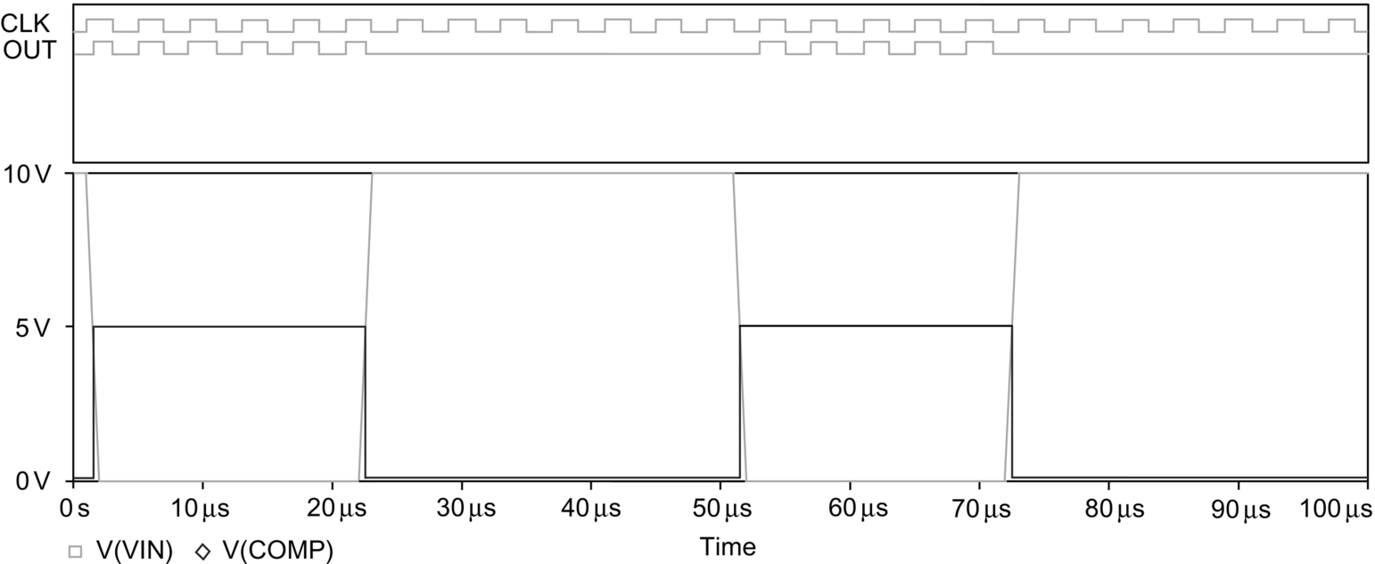
Fig. 19.1 shows an analog comparator with an open collector transistor connected to a digital gate. The pull-up resistor is connected to the digital power supply and the output ground for the comparator is connected to digital ground. Fig. 19.2 shows the digital waveforms being plotted in the upper area of Probe and the analog waveforms plotted in the lower area.

Mixed analog and digital circuits follow the same procedure for placing parts, creating a simulation profile and simulation.
19.1 Exercises
Exercise 1
Fig. 19.3 shows an AD7224 digital to analog converter (DAC) with an input digital data word of 0111 1111. From the manufacturer's data sheet, the output voltage is given by:
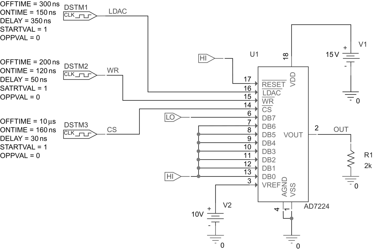
The timing cycles for the DAC have been set up according to the manufacturer's datasheet.
1. Draw the circuit in Fig. 19.3. The AD7224 can be found in the DATACONV library and the DigClock stimuli can be found in the source library.
If you have a pre 17.2 release (16.6 or before) then set up a simulation profile for a transient analysis with a Run to Time of 5 μs then select Options > Category: Gate-level simulation and set Initialize all flip-flops to 0, see Fig. 19.4. Close the Simulation Settings.

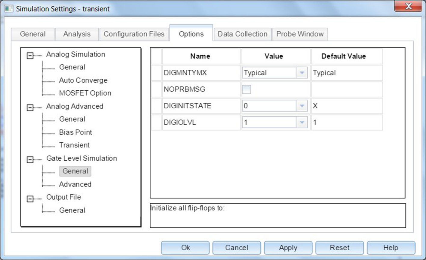
If you have a post 17.2 release (17.2 and onwards) then set up a simulation profile for a transient analysis with a Run to Time of 5 μs then select Options > Gate Level Simulation > General. Set the Value for DIGINITSTATE to 0 from the pull down menu, see Fig. 19.5. Close the Simulation Settings.
2. Place voltage markers on the nets, LDAC, WR, CS and OUT.
3. Run the simulation.
4. In Probe, you will see that the upper plot is for the digital signals and the lower plot is for the analog OUT signal (Fig. 19.6).
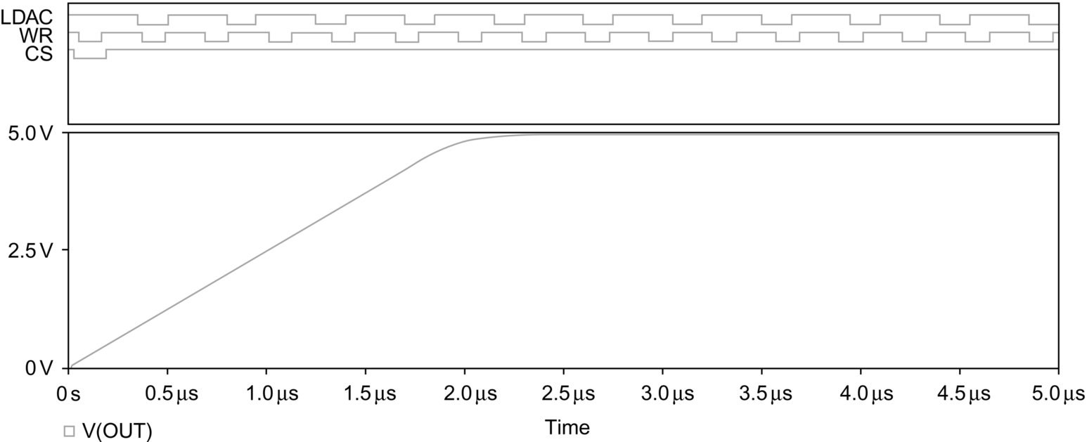
5. Turn the cursor on and check that the output voltage is 4.96 V as calculated.
Exercise 2
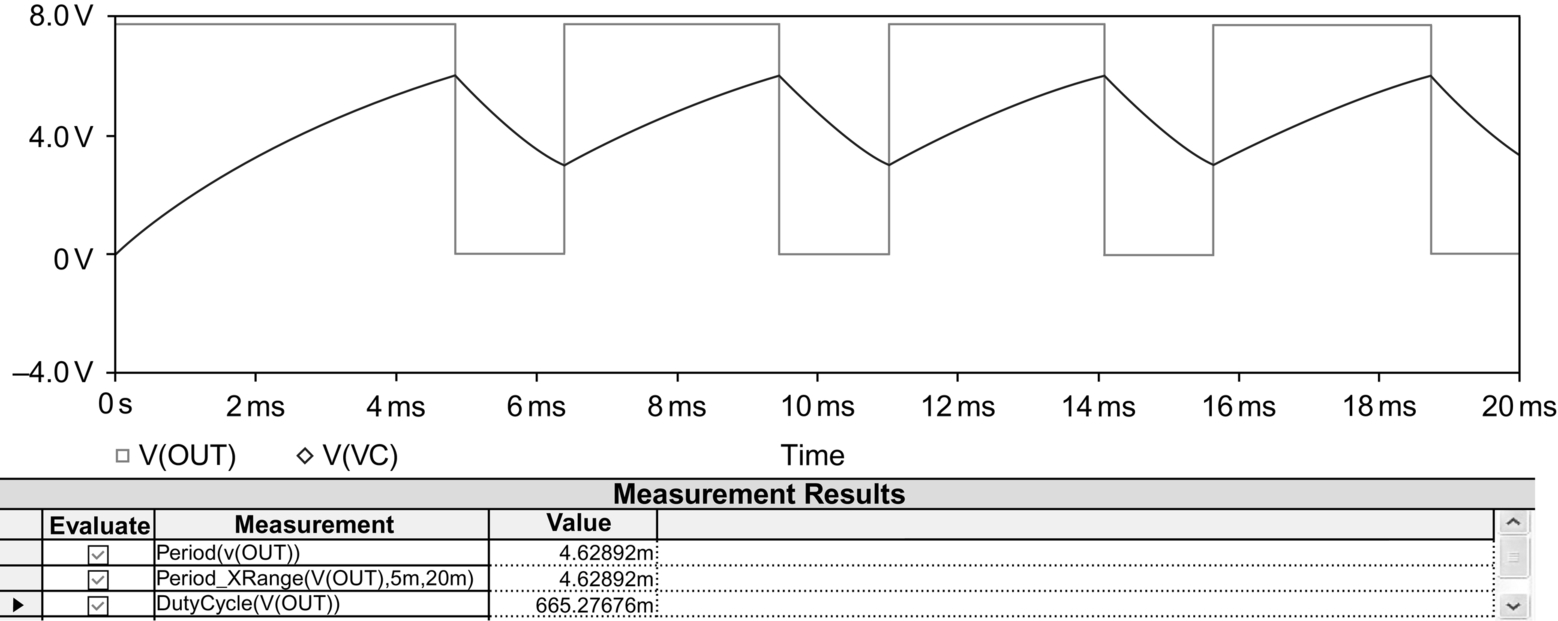
Fig. 19.7 shows the ubiquitous NE555 timer, used in countless applications. The timing equations for the NE555 are given as:
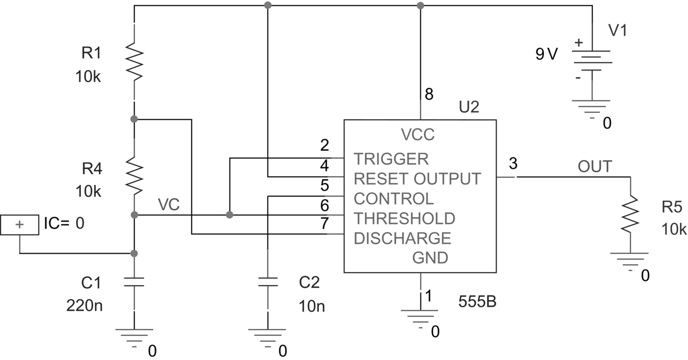


Using the components as shown in Fig. 19.7 will give a calculated clock frequency of 218 Hz and a duty cycle of 0.67.
1. Create a new project called Clock Oscillator. Rename SCHEMATIC1 to clock and draw the circuit in Fig. 19.7; the 555 can be found in the anl_misc library. There are three versions, 555alt, 555B and 555C, which have the pins arranged differently. Do not forget to place an initial condition, IC1, from the special library on C1.
2. Create a transient simulation profile for 20 ms. Place markers on VC and on OUT.
3. Run the simulation.
4. Display the cursors and determine the period of oscillation and hence the clock frequency.
5. Determine the duty cycle, which is the on time divided by the off time.
6. Confirm your measurements by selecting Trace > Evaluate Measurement and Period(1) then selecting V(OUT).
Period(V(OUT))
7. Select Trace > Evaluate Measurement and Period_XRange, (1,begin_x,end_x) then select V(OUT), and then enter 5 and 20 m.
Period_XRange(V(out),5m,20m)
8. Confirm your measurements by selecting Trace > Evaluate Measurement and DutyCycle(1), then selecting V(OUT).
DutyCycle(V(OUT))
9. If the results of the measurements are not shown, select View > Measurement Results. Your results should be similar to those shown in Fig. 19.8.
The CadenceOrCAD software installation includes a good selection of analog, digital and mixed example circuits in the anasim, digsim and mixsim directories. These can be found in the installed directory, for example:
<install path>CadenceSPB_16.3 oolspspicecapture_samples
<install path>CadenceOrCAD_16.3 oolspspicecapture_samples