
Convergence Problems and Error Messages
Abstract
PSpice uses the Newton-Raphson iteration method to calculate the nodal voltages and currents for nonlinear circuit equations. The algorithm will start off with an initial “guess” to the solution and perform an iterative process until the voltages and currents converge to a consistent solution. As discussed in the chapter on Transient analysis, at every time step, the node voltages and currents are calculated and compared to the previous time step DC solution. Only when the difference between two DC solutions falls within a specified tolerance (accuracy), will the analysis move on to the next internal time step. The time step is dynamically adjusted until a solution within tolerance is found. However, if a solution cannot be found, PSpice will report that the simulation has failed due to a convergence problem. There are also occasions where the time step becomes too small for the iteration process to continue. This can occur if there is a fast moving signal in the circuit such as a pulse with a very short unrealistic rise time.
Keywords
Nodal voltage; DC solution; Circuit; Inductor loop; Bias point; Error messages; Voltage loop; Floating node
PSpice uses the Newton-Raphson iteration method to calculate the nodal voltages and currents for nonlinear circuit equations. The algorithm will start off with an initial “guess” to the solution and perform an iterative process until the voltages and currents converge to a consistent solution. As discussed in the chapter on Transient analysis, at every time step, the node voltages and currents are calculated and compared to the previous time step DC solution. Only when the difference between two DC solutions falls within a specified tolerance (accuracy), will the analysis move on to the next internal time step. The time step is dynamically adjusted until a solution within tolerance is found. However, if a solution cannot be found, PSpice will report that the simulation has failed due to a convergence problem. There are also occasions where the time step becomes too small for the iteration process to continue. This can occur if there is a fast moving signal in the circuit such as a pulse with a very short unrealistic rise time.
Simulations can also fail because of circuit errors and missing or incorrect parameters specified. Some of these common errors will be discussed in this chapter.
8.1 Common Error Messages
Error—Node < name > is floating
There is no zero volt node “0” in the circuit. See Chapter 2, exercise 1 and Chapter 3, exercise 1.
Error—Missing DC path to ground
There is no direct DC path to ground. Add a large value resistor either to the 0 node or to a DC ground path. See Chapter 3, exercise 1.
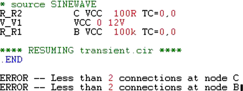
Error—Less than two connections at node < name >
There is no PSpice model attached to the Capture part. The Capture part is missing the required properties for PSpice simulation. This error can also happen if nets are left floating in that a wire is left “dangling.”
Error—Voltage source or inductor loop
Voltage sources are modeled as ideal in that they have no internal resistance therefore connecting two voltage sources in parallel will result in an infinite current which will exceed the maximum current limit. Voltages and currents are limited to ± 1e10 V and ± 1e10 A.
An inductor is essentially a time varying voltage source and if connected in parallel with another inductor or voltage source, will result in the same error message. Inductors are modeled as ideal in that they have zero series winding resistance.
8.2 Establishing a Bias Point
The Bias Point analysis is the starting point for a transient analysis and a DC Sweep. However, if PSpice cannot calculate the Bias Point for a circuit, the power supplies will be reduced from 100% toward zero where the nonlinearities of the circuit will effectively be linearized and hence improve the chances of a Bias Point solution to be found. The power supplies are then stepped back up to 100% in order to establish a Bias point upon which a DC Sweep or a transient analysis can be started.
When you run a transient analysis, PSpice launches and the simulation progress is shown in the Simulation Status Window and Output Window. Fig. 8.1 shows an example of the output window reporting that the Bias point was calculated, the transient analysis was finished, and that the simulation is complete.

The information displayed helps us to determine if the convergence failed during the Bias point analysis or the subsequent transient, DC, or AC analysis.
8.3 Convergence Issues
If there is a convergence issue, then the simulation pauses and the PSpice runtime settings window appears as shown in Fig. 8.2.
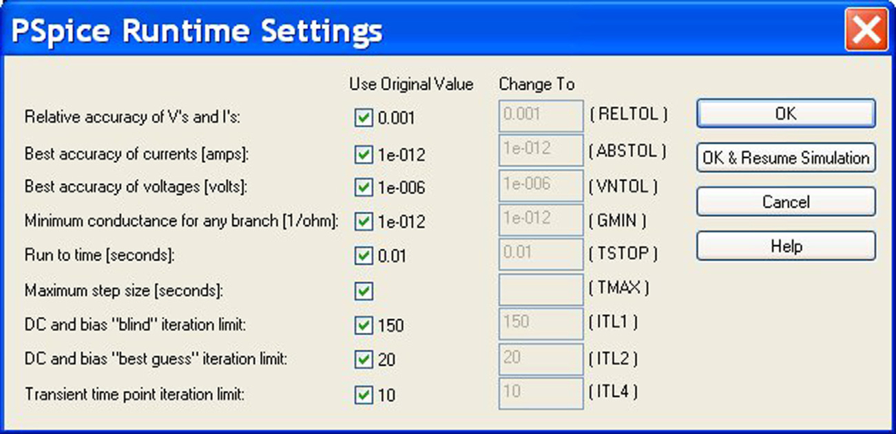
You can then change a simulation parameter and resume the simulation.
The output file will also be displayed and will report the last node voltages tried and which devices failed to converge which may relate to the nodes where the problem is.
There are no clearly defined rules for solving convergence problems. What you need to do is to try and localize the problem. For large circuits, methodically remove and simulate smaller portions of the circuit. This is where a hierarchical design, made up of blocks of circuitry, can help in solving convergence problems. Each block can be simulated separately and successively in the hierarchy, building up to the complete design. Hierarchical designs are covered in Chapter 20.
Another approach for large circuits is to replace parts of circuits with analog behaviorial models (ABM) which use mathematical expressions or tables to model components or circuit behavior. These devices simulate faster and can help localize which circuits are not converging by a process of replace and elimination. However, ABM's, if not used properly, can cause convergence problems in their own right especially if a mathematical expression contains a denominator variable which can under certain circuit conditions be set to equal zero resulting in large numbers exceeding the PSpice limits of ± 1e10 V and ± 1e10 A.
Small circuits consisting of a few components can also cause convergence problems, even the humble diode if not modeled with a series resistance can cause currents and voltages to exceed the PSpice limits of ± 1e10 V and ± 1e10 A.
Ideally the models used from semiconductor vendors are complete and have been tested for simulation and should not be the main cause of convergence problems. The only issue is that some semiconductor models are represented by a subcircuit, especially power MOSFETS which can lead to convergence problems.
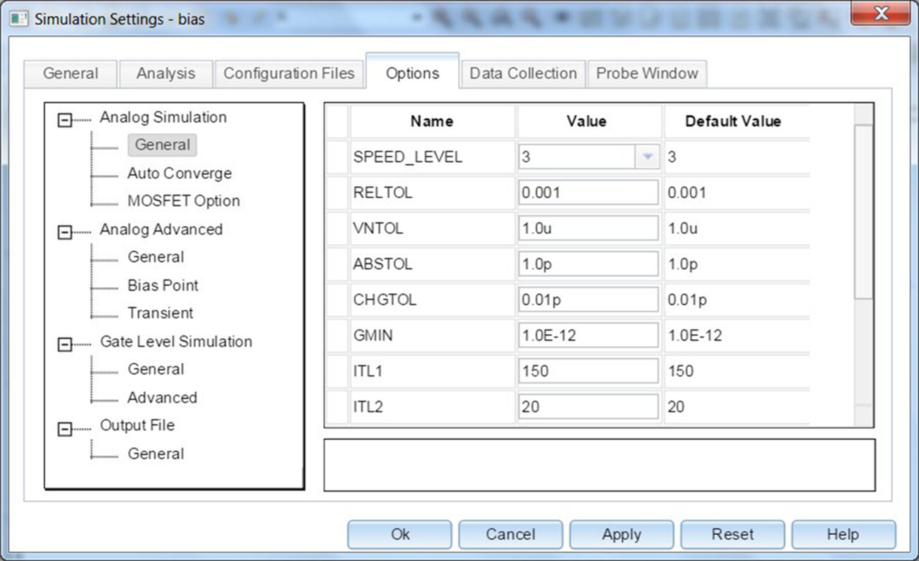
8.4 Simulation Settings Options
The simulation settings can be accessed via the simulation profile and selecting the Options tab as shown in Fig. 8.3.
The calculated voltages and currents are based on previous calculated values such that the condition for convergence, for a node voltage is given by
Similarly, for a branch current:
where RELTOL is the relative tolerance and VNTOL and ABSTOL are the absolute tolerances for voltage and currents, respectively. RELTOL has a default value of 0.001 which is equivalent to a 0.1% accuracy. Convergence will only occur when the relative difference between consecutive voltages and consecutive currents are calculated within the specified accuracy of simulation.
If you have a high voltage circuit in which the output voltage is 100 V, then using VNTOL which by default is 1 μV can be increased to 10 or 100 mV without affecting the resolution of accuracy and may help with subsequent convergence problems. The same applies to high current circuits where the default value of 1 pA for ABSTOL can be increased.
The number of times the simulator will try and reach convergence is set by the iteration limits, ITL1, ITL2, and ITL4. In some cases, just increasing the number of iteration limits will help a circuit to converge without reducing the accuracy of any of the simulation parameters. In Fig. 8.3, you can see that ITL and ITL2 are used in the calculation of the DC Bias Point and ITL4 is used in a transient analysis. When running a transient analysis it is always good idea to see if the convergence problem occurs with during the DC Bias Point calculation or the transient analysis so you can increase the appropriate iteration limit.
There is now a new feature in the simulation settings option window. Autoconverge, allows modified simulation settings to be used in a subsequent simulation run if there is a convergence problem. You enter the maximum Relaxed limit such that the simulator will automatically relax the simulation limit in an optimal manner subject to the maximum values set. The simulator will then automatically start again at time t = 0 using the modified values. Fig. 8.4A and 8.4B shows the AutoConverge settings for pre and post 17.2 software versions.

Across each semiconductor there is a small conductance which provides a small conducting path for currents such that initial currents and voltages can be calculated for the initial DC bias point solution. This conductor is called GMIN and is globally available as one of the simulation setting options shown in Fig. 8.3. This is particularly useful when you have power MOSFETS or diodes with a large off resistance. By default, GMIN is 1.0E − 12 Siemens but this can be increased up by a factor of 10 or 100. There is an option to automatically step GMIN, Use GMIN stepping to improve convergence which is very useful.
8.5 Exercises
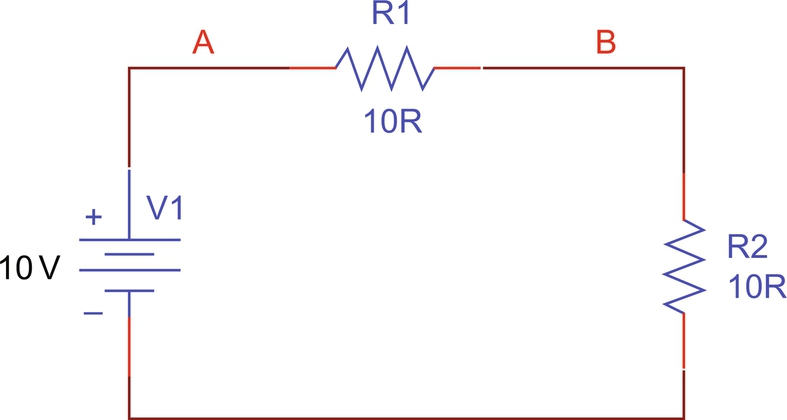
Exercise 1
1. Draw the circuit in Fig. 8.5 and create a bias point simulation, PSpice > New Simulation Profile. In the Analysis type, select Bias Point and click on OK.
2. Run the Simulation, PSpice > Run or click on the run button .
.
You should see the warning message dialog box (Fig. 8.6) and a message will be displayed asking you to check the Session Log.

The Session Log is normally open at the bottom of the screen, if not, the session log can be found from the top tool bar, Window > Session Log. The warning message will read:
WARNING [NET0129] Your design does not contain a Ground (0) net.
Click on OK and PSpice will launch.
3. In PSpice, the output file displays an error message as shown in Fig. 8.7.
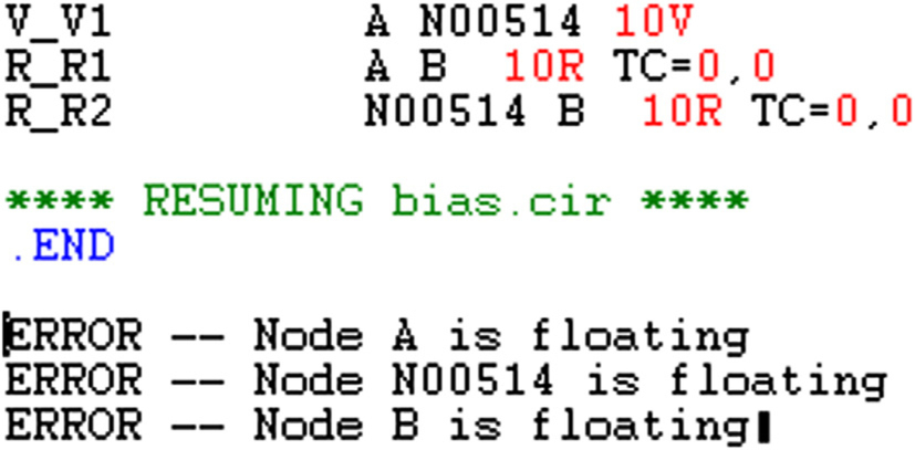
All nodes are reported as floating as there is no reference to 0 V. Connecting a ground 0 V symbol will allow the circuit to simulate.
Exercise 2
1. Draw the circuit in Fig. 8.8 and create a bias point simulation, PSpice > New Simulation Profile. In the Analysis type, select Bias Point and click on OK.
2. Run the Simulation, PSpice > Run or click on the run button.
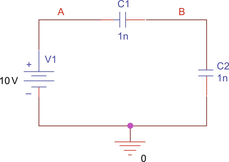
3. In PSpice, the output file displays an error message as shown in Fig. 8.9.
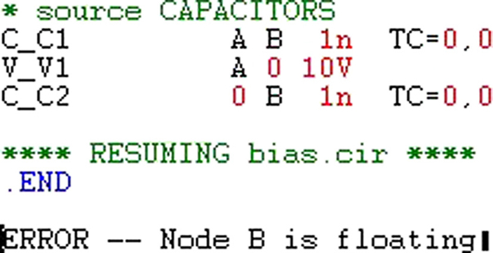
This is because there is no DC path to ground at node B which will always be the case for two capacitors connected in series. Connecting a large value resistor across R1 or R2 will allow the circuit to simulate.
Exercise 3
1. Draw the circuit in Fig. 8.10 and create a bias point simulation profile.
2. Run the simulation.
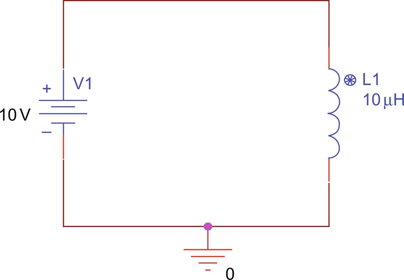
3. The PSpice output file will display an error message as shown in Fig. 8.11.

Inductors do not contain a series resistance so adding a series resistor will allow the circuit to simulate.
Exercise 4
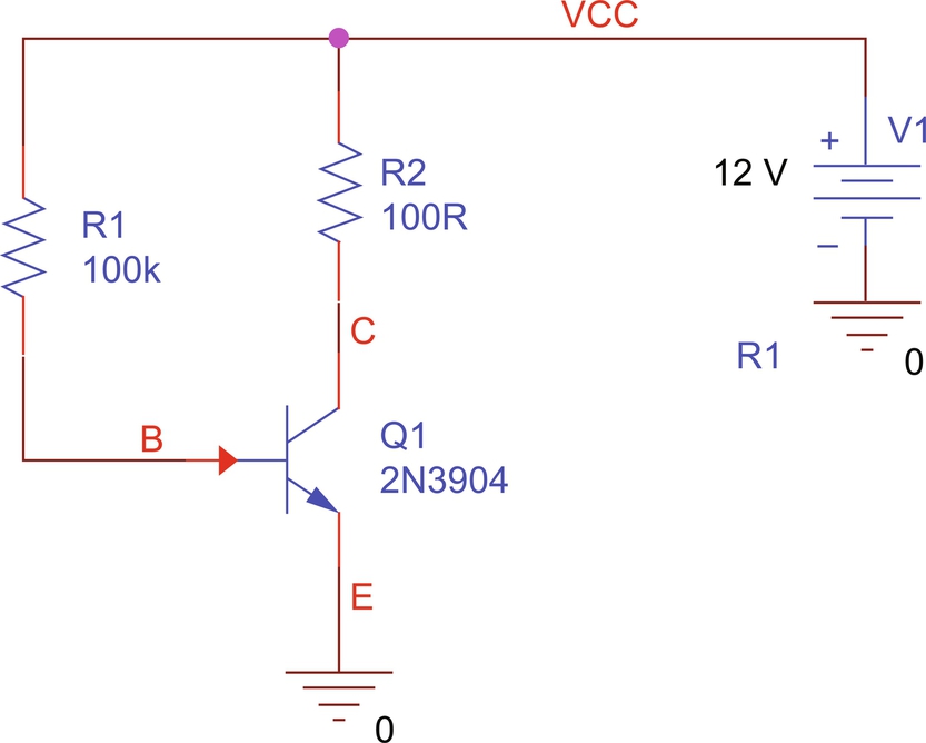
1. Draw the circuit in Fig. 8.12 using the transistor from the Capture transistor library.
2. Create a bias point simulation profile.
3. Run the simulation.
4. The PSpice output file will display an error message as shown in Fig. 8.13.
Note the transistor does not appear in the netlist.
5. In Capture a green circle will appear next to the transistor. Click on the circle and a Warning message will appear as shown in Fig. 8.14 stating that there is no PSpice template for Q1. The PSpice template is a required property for a Capture part to be simulated in PSpice. This will be covered in more detail in the Model Editor chapter.
