
An electronic die
Warning
This circuit uses members of the integrated circuit family known as CMOS (complementary metal-oxide semiconductor). These use very little current and can be completed destroyed if they come into contact with the magnitudes of static electricity that most of us carry about when we walk on carpets and wear rubber shoes. You will never know if this wanton destruction has happened – all you will discover is that your circuit doesn’t work and that you have tested everything. To avoid this problem do the following things:
1. Before you open the little packet in which the IC is supplied, touch something which you know to be earthed – the metalwork of any equipment which is mains-earthed, for example. Then open the packet.
2. Let the IC fall gently on the bench – don’t pick it out with your fingers. Touch your earthed metalwork again. Pick up the IC and insert it gently into its holder.
The circuit is safe from damage while it is connected to the battery.
Description
The circuit is shown in Figure 1. IC1a and IC1b form an astable multivibrator, similar to that used in ‘An LED Flasher’ also in this book. It runs constantly, and its output is fed to IC2 via a single NAND gate, IC1c. The other input of IC1c is held at 0 V by R3 and C3. Whenever one input of a NAND gate is logic 0 (or 0 V), there can be no output from the gate, irrespective of what is happening at other inputs. So, despite the fact that the oscillator (or clock) is running all the time, its square-wave output never reaches IC2 until the ‘other’ input of IC1c is brought away from logic 0. This happens when SW2 is pressed. Pressing SW2 momentarily, as is normally done, charges up C3 to 9 V, putting a logic 1 on the second input of IC1c and allowing the clock signal through to IC2. As the switch is released, C3 begins to discharge through R3, gradually lowering the voltage on pin 8 of IC1c. As this voltage crosses 4.5 V (half the supply voltage), IC1c then treats this input as logic 0, which cuts off the clock signal from IC2 again. Thus, when SW2 is momentarily pressed, the clock signal is fed to IC2 for a short interval of time, before being blocked again.
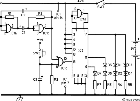
IC2 is a binary counter, and the outputs that concern us are from pins 14, 11 and 6. Pin 14 is the most significant bit and pin 6 the least significant bit. See the panel for an explanation of what happens here.
As the clock cycles are counted, the LEDs flicker as the die is ‘rolled’. Resistors R4 to R7 are used to limit the current through the LEDs. When the counter stops, it can be in any of the positions shown in Table 1. Because of the way in which the dots are grouped on the faces of a die, the wiring of the LEDs is simpler than it might otherwise be. You can see from Figure 1 that there are really only three sets of connections to the LEDs – one from each bit of the counter output. When pin 14 is at logic 1, four LEDs are lit, corresponding to the number four. For the number five, pins 14 and 6 will be at logic 1. For the number one, only pin 6 is at logic 1. For three, pins 11 and 6 are at logic 1, for six, pins 14 and 11 are at logic 1, and for two, only pin 11 is at logic 1. These conditions are summarised in Table 1.

Construction
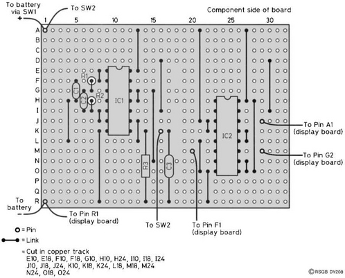
Two pieces of Veroboard (of the strip type) are needed – one for the main circuit (Figure 2) and the other for the display LEDs (Figure 3). The display board is easier to build, so we will do that first. It measures 20 holes by 18 strips.
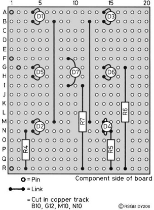
Cut the tracks as shown in Figure 3, using a 3 mm (![]() ) twist drill rotated between thumb and forefinger. Insert and solder the Veropins, resistors and the wire links. Then solder the LEDs in place, making sure their polarities are correct. The LEDs are mounted proud of the board (Figure 4, which will help when you come to fix the board into a case.
) twist drill rotated between thumb and forefinger. Insert and solder the Veropins, resistors and the wire links. Then solder the LEDs in place, making sure their polarities are correct. The LEDs are mounted proud of the board (Figure 4, which will help when you come to fix the board into a case.

The main board measures 32 holes by 18 strips. As before, remove the tracks in the places shown in Figure 2. Note that track ‘L’ is not broken under the position for IC2. Solder in the IC holders and the links. Solder in R1 and R2 vertically, and R3 horizontally. Then solder in C1, C2 and C3; these all being electrolytics, check their polarities. Solder in the Veropins and prepare the connections to those components not on the main board, using stranded, insulated wire. Check the circuit carefully, and read the handling precautions given earlier before carefully inserting the two ICs.
Testing and use
When the circuit is switched on, it is likely that the centre LED only will be lit. Press SW2, the ‘throw’ switch. All the LEDs should flicker, even after the switch is released, but only for a second or so. Then a standard pattern should show, signifying numbers between one and six. If this does not happen, switch off and check your circuit again. Are there any missing links? Are there any obvious dry joints (usually dull instead of shiny)? Can you see any solder bridges between tracks? Did you choose to ignore the handling precautions? If none of these results in a working circuit, try some fault-finding.
• Disconnect the lead to D7 on the main board (marked ‘to pin F1’ on Figure 2). Touch the lead on to the positive supply rail. D7 should light. Now transfer this lead on to pin 4 of IC1. If it flickers, then the oscillator is running (which it should).
• Transfer this lead to pin 10 of IC2. D7 should flicker when SW2 is pressed, but should be on permanently when it is released. This means that the correct signals are reaching IC2 from IC1.
• If one of the chains of LEDs (i.e. D1 and D2, D3 and D4, D5 and D6) does not light, you may have one or both LEDs the wrong way round.
When the die is working, you may care to experiment with the values of R1 and R2, but you should keep their values the same, i.e. R1 = R2. The larger the values of these, the more slowly the die will appear to ‘roll’.
Finishing touches
On completion of the project, you will want to mount it in a smart case; any plastic box is suitable for this, with the display board mounted so that the LEDs protrude through the top and are fixed to it using LED clips. The way in which you mount both boards to the case is entirely up to you.