
CW QRP transmitter for 80 metres
The circuit
Like other simple transmitters (see An 80 Metre Crystal-Controlled CW Transmitter and A Breadboard 80 m CW Transmitter elsewhere in this book) this one is crystal controlled. This assures frequency stability, but limits the usefulness of the transmitter. The key to increased frequency coverage without a conventional Variable Frequency Oscillator (VFO) is the use of a low-cost 3.58 MHz ceramic resonator. The ‘pulling’ range of a 3.58 MHz ceramic resonator covers the UK novice 80 m sub-band and some of the CW segment below 3.525 MHz.
A ceramic resonator is like a crystal, but not quite as stable in frequency. Its main advantage is its large pulling range.
The block diagram is shown in Figure 1. It is very similar to a crystal-controlled transmitter, and includes an oscillator, buffer and final amplifier.
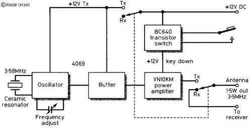
This amplifier is keyed, the oscillator remaining running all the time. This improves frequency stability because the oscillator is not being continuously stopped and started by the key. It is switched off while receiving, though, to avoid interference with the received signal. Transmit/receive switching is accomplished by a panel-mounted switch controlling both the aerial, oscillator and buffer switching.
Figure 2 shows the transmitter circuit diagram. An unusual aspect of this transmitter is the use of a digital CMOS integrated circuit (IC) type 4069 for the buffer and oscillator stages. The IC houses six inverters, four of which are used in the circuit. One is used as the oscillator, two are used for the buffer stage, and the fourth provides an output for a direct-conversion receiver, should one be added at a later date.

The frequency of the oscillator is changed by varying the capacitance in the ceramic resonator circuit. This is provided by VC1.
The power amplifier (PA) is a small MOSFET (metal oxide semiconductor field-effect transistor), TR1. This is capable of providing an output power of 2 W but, in this circuit, it is run conservatively to give 1.5 W. The output can be varied by changing the resistance (R5 + R6) in the gate circuit. Attempts to raise the output power by decreasing the values of these resistors may result in immediate MOSFET failure.
A pi-network (C8, RFC, C9) provides impedance matching to 50 Ω, together with harmonic suppression. Like all inductors in this transmitter, the pi-network inductor is a pre-wound RF choke. A pi-network is so called because the components are arranged in the shape of the Greek letter pi (π).
Keying is carried out by a pnp transistor switch, TR2. Closing the key earths the base and supplies 12 V to the collector of TR2 and to the drain of the MOSFET, TR1, allowing the PA to operate.
Construction
You must house your transmitter in a metal box, to avoid hand-capacity effects and the radiation of spurious frequencies. Size is not important, provided it is large enough to accommodate the transmitter without cramping the components. You may want to allow space for future additions such as a direct-conversion receiver, break-in keying, sidetone or a small power amplifier. A good size is 5 × 15 × 15 cm. You can make your own box, buy it, or even use a biscuit tin!
Front and rear panel connectors can be fitted first. The choice of these is a personal matter, but a good working choice would be:
(a) Power socket – 2.1 mm panel socket – centre pin positive.
(b) Key socket – ¼ inch jack socket.
(c) Aerial and receiver connectors – panel-mounting SO239 type.
Particular attention must be paid to the mounting of the variable capacitor, VC1. Make sure the hole for the shaft is amply big enough, and if you use screws to mount the capacitor on the front panel, then make sure they are not too long, otherwise they will touch the vanes of the capacitor! Mounting can be by means of glue, sparingly applied and kept well away from the shaft.
A board size of about 6 × 10 cm is adequate. Component layout on the board is suggested in Figure 3. The prototype used ordinary matrix board, which is preferable to stripboard for a design like this; stripboard has undue capacitance between adjacent strips. Component leads are fed through holes in the board and are connected underneath. Make sure that leads and connections are rigid because, if they can move, there is always the danger of short-circuiting, and capacitance changes.

Figure 3 Component layout of the 80 metre transmitter. The transmit/receive switch is not mounted on the board and is not shown in this diagram
To facilitate construction, servicing and testing, it is advisable to use Veropins for connections to the variable capacitor, transmit/receive switch, aerial and power sockets. Use screws and spacers to mount the circuit board to the box. Mounting the board horizontally assists troubleshooting.
Use a socket for the IC, and observe the CMOS handling precautions given in An Electronic Die, elsewhere in this book. When soldering the leads to the ceramic resonator, do it quickly – excessive heat damages the device. The earth lead running acoss the bottom of the board must be connected to the metal case by a short length of stout wire.
Testing
After carefully checking your wiring, both against the circuit diagram and the layout diagram, it is time to test your circuit. You will need a multimeter, an 80 m SSB receiver and a 50 Ω dummy load. A good design of dummy load can be found in the project A Switched Dummy Load, also in this book. An RF power meter and frequency counter will also be useful, although if your receiver has a digital frequency readout and S-meter, the latter two items are not really necessary. You will also need a 12 V 1 A power supply unit (PSU) to power the transmitter.
Switch the transmitter to receive and switch on the transmitter. No current should be consumed. Switch to transmit and check that pin 14 of IC1 is 6.8 V positive. With the dummy load connected to the aerial socket, press the key. The voltage on TR2 collector should now be 12 V, dropping to zero when the key is released.
Now check the operation of the oscillator. In transmit mode, you ought to be able to find a strong carrier signal with the receiver, even though the dummy load is connected. Adjusting the variable capacitor should change the frequency. At the lower end of the frequency range, you may find that the oscillator is unreliable in starting, because the circuit is attempting to pull the resonator too low in frequency. If this is the case, set the trimmer at the back of VC1 to minimum capacitance. If your version of VC1 has two trimmers, and you don’t know which one to set, set them both to minimum capacitance. If there is still a problem, reduce the value of RFC1 to 6.8 or 4.7 μH.
In all probability, the unmodified circuit of Figure 2 will not require any of the changes outlined here. A coverage of 3.518 to 3.558 MHz should be possible, while preserving good frequency stability and reliable oscillation.
A signal probe (see An RF Signal Probe, elsewhere in this book) is useful for checking the operation of the oscillator and PA. Alternatively, an RF power meter or the receiver’s S-meter can be used. With the PA running, the unit should draw between 200 and 300 mA. If TR1 becomes too hot to touch after a few seconds of transmitting, increase R5 or R6 to limit the transistor’s heat dissipation. A small 6.3 V bulb connected across the aerial output is a simple way to check that the PA is working. An orange/white glow when the key is pressed is indicative of correct operation.
The final test is to monitor keying ‘quality’. With your dummy load connected, press the key and listen to the note on the receiver’s loudspeaker. Then operate the key, sending a string of dits, for example. What you hear should be free of chirps and clicks, as well as being stable in frequency. This test is sometimes better performed with no aerial connected to the receiver, thus preventing receiver overload and its associated plops. No problems should be encountered here.
Frequency tuning
A peculiarity of ceramic resonators is that, every now and again, their frequency changes abruptly by 100 Hz or so, then remains stable for some time. This is certainly noticeable in the received signal, but does not detract from the QSO and no characters are lost as a result. Try to keep the area around the ceramic resonator cool, to avoid temperature variations.