CSU/DSUs are like bridges. They have one interface in telco territory and one interface in data-communications territory. Both are serial interfaces that make use of tight timing tolerances. Appropriate configuration of the CSU/DSU to work within the timing straitjacket is essential.
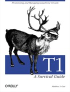
In the T1 world, clock signals are not transmitted separately from the data stream. Instead, receivers must extract the clock from the data signal based on the stream itself. Each bit time slot is 648 nanoseconds. Pulses are transmitted with a 50% duty cycle, meaning that for the middle half of the time slot, the voltage is at its peak. Based on these characteristics, the receiving CSU/DSU infers time slot boundaries from incoming pulses. Ideally, each pulse comes in the middle of a time slot, so finding time-slot boundaries is simply a matter of going 324 ns in each direction. Figure 5-3 illustrates clock inference from pulse reception.
In practice, of course, things are never quite as simple, and CSU/DSUs must compensate for a variety of non-ideal conditions. Clock signals may exhibit both short-term and long-term irregularities in their timing intervals. Short-term deviation is called jitter, and long-term deviation is referred to as wander.
Tip
Timing on the T1 network interface from the telco is implicit and based on the content of the pulse stream. On the other hand, the serial circuit that connects the CSU/DSU to the router makes use of explicit timing. V.35, for example, includes two pairs (four leads) for sending timing signals and one pair (two leads) for receiving timing.
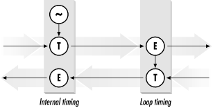
At the interface to the telco network, clocking on the received data is based on inferring where the bit times fall. The CSU/DSU does not send an explicit clock for use with transmitted data, but uses internal circuitry to determine when to send a pulse. The internal clocking circuitry can typically operate in one of three modes, which go by different names for different vendors. Descriptively speaking, the typical modes of operation are to derive the transmit clock from the telco, to use an internally generated timing signal, or to take the transmit clock from the attached DTE. Of the three options, the first two are by far the most common in data-transmission applications.
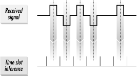
In master/slave timing, the CSU/DSU takes its timing from the telco network. The telco network maintains an extremely accurate timing source and uses that to send pulses to customer locations. At the customer CSU/DSU, the receive clock is extracted from the incoming pulses. In master/slave timing, the extracted receive clock is used for the transmit clock on the network interface, as shown in Figure 5-4.
Master/slave timing ensures that the less-accurate clock in the customer premises equipment does not drift significantly, relative to the telco’s accurate timing system. Several sources may drive the telco transmit clock. One common source is the building-integrated timing supply (BITS), which ensures that all the equipment in the CO is running from the same signal. BITS can be linked to an external clock, illustrated in Figure 5-4 as the PRS. At the customer side of the link, the CSU/DSU extracts the receive clock, rather than relying on an internal oscillator in the CSU/DSU. Master/slave timing is also called loop timing because the clock is extracted from signals on the digital loop, or network timing because the clock source is from the telco network interface.
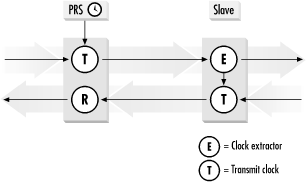
Internal timing uses an internal oscillator in the CSU/DSU as the transmit clock source. No special measures are taken to ensure that the timing of transmitted pulses matches the timing of received pulses because the two operations are logically independent, as Figure 5-5 illustrates.
All circuits must have one timing source. In most cases, the telco will supply timing because the entire telco network must operate with unified timing to deliver the T1 circuit. In some cases, however, a simple copper wire pair can be leased from the telco. For spans with less than 30 dB attenuation, an unrepeatered copper pair can cost much less than a full-service line. In private-line applications, one end of the line must provide the clock, as Figure 5-6 shows. The remote end is set to loop timing, so the remote transmit clock is derived from the local transmit clock.
Data ports on CSU/DSUs are synchronous serial ports. CSU/DSUs transmit data as a varying voltage on the line, with a high voltage representing one and a zero voltage used for zero. A second signal, the clock signal, triggers a voltage measurement and extracts a bit from the voltage stream. Figure 5-7 illustrates the use of the explicit clock signal on a synchronous serial port.
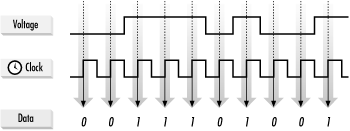
In Figure 5-7, the external clock signal triggers a measurement when the clock signal goes from a low voltage to a high voltage. Aligning the clock signal with the voltage plateaus is important. Ideally, the clock signal should trigger a voltage measurement at the middle of the bit time. If the clock signal falls too close to a voltage transition, the reading will be unreliable.
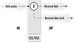
The clocking on the serial circuit from the CSU/DSU to the router is a synchronous serial line that uses explicit timing. Clock signals for the received data are extracted from the incoming pulse train at the carrier network interface. The extracted data is then transmitted with the extracted clock signal out the data port. No configuration is necessary on T1 equipment to configure the clock signal for received data. Figure 5-8 demonstrates receive clock timing.
Forwarding the received data out the data port and on to the router is only half of what a T1 does. Transmitting data from the data port out to the telco network successfully requires that the data be correctly received from the data port and processed accurately. The simplest clocking method is to allow the CSU/DSU to control the clocking of transmitted data, too. V.35 interfaces allow the CSU/DSU to supply timing to the DTE. Data arrives at the CSU/DSU and is then extracted using the transmit clock supplied to the DTE, as Figure 5-9 illustrates.
In most applications, internal data port clocking provides acceptable performance. If the clock signal drifts out of phase with the data transmission, however, the clock will trigger measurements too close to the transition between the high voltage and the low voltage. Measurements to extract bits still take place, but those measurements may not reflect the data that was supposed to be transmitted. Figure 5-10 illustrates the problem.
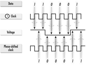
As in Figure 5-7, the clock signal triggers a measurement at the rising edge. The lower clock signal is delayed, or phase shifted, so measurements occur too late and extract incorrect data. One common reason for the delay is a long cable between the CSU/DSU and the router. The router synchronizes its transmissions with the transmit clock, but the data must travel from the router to the CSU/DSU. In the time it takes for the data to travel along the cable to the CSU/DSU, the clock signal has moved on and the measurements it takes are tardy. Problems may also occur at high-transmission rates, because the bit times are shorter, or when the router has a significant processing latency.
One way to address the problem of a phase-shifted clock signal is to change the source of the transmit clock at the data port. Routers can be designed to accept the transmit clock from the CSU/DSU and use it to drive the external clock line. The external clock line is often labeled XCLK or SCTE (an abbreviation for serial clock timing external). The router assumes the responsibility of synchronizing the transmitted data with the external clock signal. With external clocking, the clock and data must take the same path and are subject to the same delays, so the data and its clock signal stay in phase over the cable. This is illustrated in Figure 5-11.
Many routers, however, do not support looping the received clock signal back to the CSU/DSU. When these routers are used with a CSU/DSU that expects a transmit clock, nothing will be transmitted because no clock signal is transmitted to the CSU/DSU.
Warning
Using a router that does not supply a transmit clock with a CSU/DSU can be a particularly difficult problem to pinpoint without the right equipment. Protocol analyzers that tap into the V.35 connection between the CSU/DSU and the router may not see a problem because the V.35 connection is fine.
This often manifests itself as a router that insists that it is transmitting data even though nothing is received by the remote end. Because nothing can be transmitted, the link layer protocol cannot initialize the link. If you see this symptom, check with the router’s vendor to ensure that they support sending a timing signal to the V.35 DCE.
A second method of addressing a phase shift between the transmitted data and its clock signal is to invert the internal clock, which has the effect of shifting the clock signal by a half-cycle. The goal of clocking on the serial port to the router is to make sure that the clock signals trigger bit extractions in the middle of the bit time. Problems occur when the clock fires at the edge of a bit time. Moving the clock trigger half a cycle returns the clock signal to the middle of the bit time.