V.35 is an old specification that has been obsolete since 1988. Most “V.35” interfaces are actually V.36, V.37, or V.38 interfaces. V.35 is fairly sparse—it does not even specify the form factor of the interface. ISO 2593 contains the specifications for the blocky, long-pinned Winchester connector. However, the industry refers to such interfaces and cables as V.35, so I will too in order to maintain consistency.
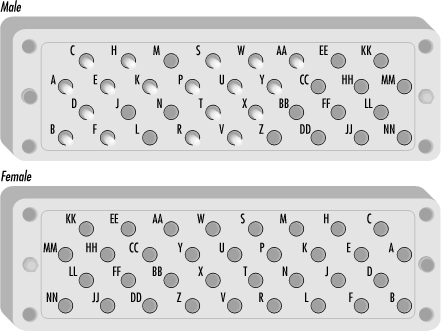
To save space, V.35 uses common-ground transmission on signaling leads, but the data and clock signals use differential signaling. Connectors have 34 possible pins, which are lettered A through NN. (G, I, O, and Q are not used.) When used for data-communications applications, connectors typically only have 17 or 18 pins. To ensure that the cables are inserted correctly, the screw attachment mechanism allows connectors to be attached only one way. Figure E-4 shows male and female V.35 connectors.
Each pin is given a purpose and is assigned to a particular serial circuit. Figure E-5 shows the circuit assignments by abbreviation. More detail on the circuits is in Table E-2.
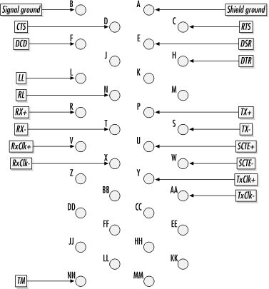
Table E-2. V.35 pin assignments
|
Pin |
V.24 circuit |
Circuit name |
Circuit abbrev. |
Circuit type |
Circuit direction |
|---|---|---|---|---|---|
|
A |
101 |
PGNDSHD |
Ground |
N/A | |
|
B |
102 |
GND or SGND |
Ground for common-ground circuits |
N/A | |
|
C |
105 |
RTS |
Common-ground control |
To DCE | |
|
D |
106 |
CTS |
Common-ground control |
From DCE | |
|
E |
107 |
DSR |
Common-ground control |
From DCE | |
|
F |
109 |
RLSDDCD |
Common-ground control |
From DCE | |
|
H |
108.2 |
DTR |
Common-ground control |
To DCE | |
|
L |
141 |
LL |
Common-ground control |
To DCE | |
|
N |
140 |
RL |
Common-ground control |
To DCE | |
|
P |
103 |
TD ATX+, SD+ |
Differential Data |
To DCE | |
|
R |
104 |
RD ARX+, RD+ |
Differential data |
From DCE | |
|
S |
103 |
TD BTX-, SD- |
Differential data |
To DCE | |
|
T |
104 |
RD ARX-, RD- |
Differential data |
From DCE | |
|
U |
113 |
SCTE A |
Differential timing |
To DCE | |
|
V |
115 |
SCR ART+ RxClk+ |
Differential timing |
From DCE | |
|
W |
113 |
SCTE B |
Differential timing |
To DCE | |
|
X |
115 |
SCR BRT-RxClk- |
Differential timing |
From DCE | |
|
Y |
114 |
SCT AST+TxClk+ |
Differential timing |
From DCE | |
|
AA |
144 |
SCT BST-TxClk- |
Differential timing |
From DCE | |
|
NN |
142 |
TM |
Common-ground control |
From DCE |
Even though Pin NN, the Test Mode signal, can occasionally be used, it is not frequently pinned out. Pin J, the Received Line Signal Detector (RLSD) is not used and not pinned on data communications equipment. Pins M, Z, BB, CC, DD, EE, FF, and MM are reserved for future standards and are not pinned. Pins HH, KK, JJ, and LL are reserved for country-specific features, but are not pinned out.
In T1 circuits, V.35 runs at 1.5 Mbps. Do not be tempted to save money by making your own cable according to a manufacturer pinout. V.35 needs to run fast within tight electrical tolerances. Hand-built cable will not work. Any money saved by scrimping on cable will haunt you when the cable turns out to have a slightly flaky lead or improper grounding.
Long V.35 connections may cause problems if the ground level at the two ends of the connection is too different. If a voltage differential exists between a third-floor router and a basement CSU/DSU, control signals may not be interpreted correctly.