
19
8212 Non-Programmable 8-Bit I/O Port
![]() Working of 8212
Working of 8212
![]() Pin diagram of 8212
Pin diagram of 8212
![]() Intel 8212 in mode 0
Intel 8212 in mode 0
![]() Intel 8212 in mode 1
Intel 8212 in mode 1
![]() Applications of 8212
Applications of 8212
![]() Applications of 8212 in mode 0
Applications of 8212 in mode 0
![]() Applications of 8212 in mode 1
Applications of 8212 in mode 1
![]() Questions
Questions
So far we have discussed in detail about 8085 microprocessor. Interfacing of memory to a microprocessor has also been discussed. Now we will discuss how I/O ports are used in a micro-computer. This chapter will present a detailed explanation of the working and application of the non-programmable I/O port, 8212.
 19.1 WORKING OF 8212
I/O ports are of two types. Programmable I/O ports and non-programmable I/O ports. Programmable I/O ports are more popular because their function can be changed by software. There is no need to change the wiring or the hardware to change the function of the I/O port. A very popular programmable I/O port chip is the Intel 8255. It will be discussed in detail in the next chapter.
On the other hand, non-programmable I/O ports require change of wiring or hardware to change its function. An example is Intel 8212, which is the topic of this chapter. As will be seen later, connection has to be changed if the 8212 has to work as an input port instead of an output port. Such non-programmable I/O ports are simple in design.
19.1.1 PIN DIAGRAM OF 8212
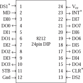
The 8212 is available as a dual in-line package chip with 24 pins. Its functional pin diagram is illustrated in Fig. 19.1. The actual pin diagram of 8212 is provided in Fig. 19.2.
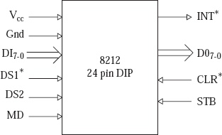
Fig 19.1 Functional pin diagram of 8212
It works on a dc supply of + 5 V. The 8-bit latch in 8212 receives information present on DI7-0 (data inputs). The condition for latching the information present on DI7-0 depends on the logic state of the MD (mode) pin. The information present in the latch comes out on DO7-0 (data output) pins. The condition to be satisfied for the latched information to come out depends on the MD pin.
There is an edge-triggered D-type flip-flop in the 8212. It is called the service request flip-flop. It is mainly responsible for generation of an interrupt request on INT*. INT* is an active low output pin, which is useful in interrupt-driven data transfer. The internal architecture responsible for activation of INT* signal is shown in Fig. 19.3.
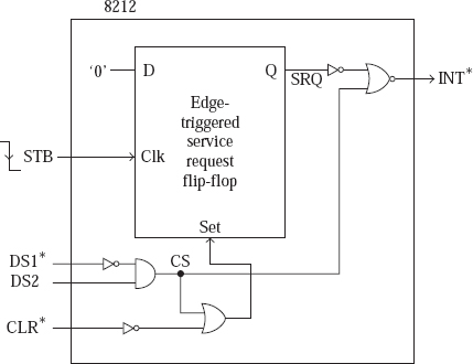
Fig. 19.3 Circuit for activation of INT* in 8212
It can be seen from Fig. 19.3 that INT* is activated in the following two cases.
- When DS1* = 0 and DS2 = 1 so that the internal CS (chip select) signal is activated.
- When STB makes a high to low transition so that the internal SRQ (Q output of service request flip-flop) signal becomes 0.
INT* is deactivated when CS signal = 0 and SRQ = 1. SRQ becomes 1 whenever CLR* = 0 or CS = 1.
Details of connection inside the 8212 for a latch flip-flop are shown in Fig. 19.4. There are eight such latches in 8212. They are all level-triggered D-type flip-flops.
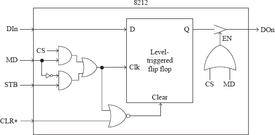
Fig. 19.4 Connecton details for a latch flip flop in 8212
The following conclusions can be drawn from Fig. 19.4. If MD = 1, CS acts as the clock for the latches. If MD = 0, STB acts as the clock for the latches. As long as the clock is in a high state, the Q output of the latch follows the corresponding DI input. When the clock makes high to low transition, the data gets latched. The data at the Q output comes out on the corresponding DO pin when the internal EN (enable) signal is activated. The EN signal is activated whenever CS = 1 or MD = 1.
Brief summary of the pins of 8212 is provided in the following.
19.1.2 INTEL 8212 IN MODE 0
Figure 19.5 explains the working of 8212 in mode 0.
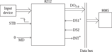
Fig. 19.5 working of 8212 in mode 0
This mode is generally used when we want the 8212 to function as an input port. An input device may be connected to DI7-0, and the microprocessor can receive the information on DO7-0. In this mode STB acts as the clock for the latches. The 8-bit latch in 8212 follows the information present on DI7-0 as long as STB = 1. When STB makes a high to low transition, the 8212 latches the information on DI7-0. High to low transition of STB activates INT* so that interrupt-driven data transfer may be performed if desired. The 8-bit latched information comes out on DO7-0 only when the output buffers are enabled. The output buffers are enabled when DS1* = 0 and DS2 = 1.
This mode can also be used when we want the 8212 to function as an output port. In such a case, STB is used by the microprocessor to load the latches with the data to be output. Output device receives the data by activating DS1* and DS2. However, mode 1 operation is more commonly used for output port function.
19.1.3 INTEL 8212 IN MODE 1
Figure 19.6 explains the working of 8212 in mode 1.
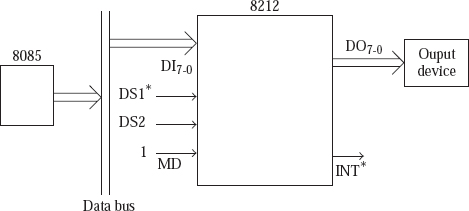
Fig. 19.6 Working of 8212 in mode 1
This mode is generally used when we want the 8212 to function as an output port. In this mode, microprocessor may drive DI7-0, and an output device may receive the information on Do7-0. CS provides the clock to the latches in this mode. The 8212 latches the information on DI7-0 when CS makes high to low transition. The activation of CS signal activates INT* so that interrupt-driven data transfer may be performed if desired. The output buffers are always enabled in this mode. So the 8-bit latched information straightaway comes out on Do7-0 without any condition.
19.2 APPLICATIONS OF 8212
Intel 8212 can be used in a variety of applications, limited only by the ingenuity of the user. A few applications are indicated below for both mode 0 and mode 1 operations.
19.2.1 APPLICATIONS OF 8212 IN MODE 0
Following applications of 8212 in mode 0 operation will be discussed.
- Gated buffer;
- Bi-directional bus driver;
- Interrupting input port;
- RSTn interrupt instruction port;
- As supplier of eight RST instructions.
Intel 8212 as gated buffer: Whenever 8212 works in mode 0, it converts a weak logic signal to a strong logic signal. The 8212 outputs in mode 0 are capable of sinking 15 mA in 0 state, and providing a minimum high output voltage of 3.65 V in 1 state. Intel 8212 is driven properly even if the input signal is capable of driving 0.25 mA only. Thus, the 8212 when working in mode 0 acts as a buffer. Intel 8212 as a gated buffer is indicated in Fig. 19.7.
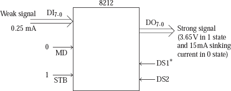
Fig. 19.7 8212 as a gated buffer
We connect STB to logic 1 so that the latch inside 8212 follows the data on DI7-0. It will come out as a strong signal on Do7-0 only when DS1* = 0 and DS2 = 1, justifying the name for the application.
Bi-directional bus driver: Sometimes it is necessary to have bi-directional buffering. Such is the case with the data lines of a microprocessor. This can be achieved using two 8212s, as shown in Fig. 19.8.
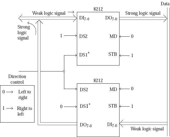
Fig. 19.8 8212 bi-directional bus driver
Both the 8212s are operated in mode 0. It may be noticed that they are connected as gated buffers. When direction control = 0, DS1* becomes 0 for upper 8212, and so the weak logic signal on the left gets transmitted to the right as a strong logic signal.
When direction control = 1, the output buffers of upper 8212 get tristated, but the output buffers of lower 8212 get enabled as DS2 becomes 1. So the weak logic signal from the right gets transmitted to the left as a strong logic signal.
Interrupting input port and RSTn interrupt instruction port: Figure 19.9 illustrates these two applications of 8212. The first 8212 is working as an interrupting input port. It performs data transfer with the microprocessor, after interrupting it. The second 8212 supplies RSTn code to 8085 in response to INTA* from 8085, when the first 8212 interrupts the 8085 on INTR pin.
When input device has some data on DI7-0, which is to be sent to the accumulator of 8085, it sends a positive pulse on STB of first 8212. When STB makes a high to low transition, first 8212 latches the information on DI7-0. Also the high to low transition of STB causes INT* to become 0. This interrupts 8085 on INTR pin after inversion.
In response to INTR, 8085 sends logic 0 on INTA*. The second 8212 receives it on DS1*. For the second 8212, DS2 is tied to logic 1. On DI7-0 of this 8212, RSTn code is wired up. As STB of this 8212 is tied to logic 1, RSTn code is available in the latch of this 8212. Thus when INTA* becomes 0, it activates DS1*, and so the RSTn code comes out of the second 8212 and enters the IR register of 8085.
Now 8085 branches to n * 8. At this location, there is a jump instruction to jump to say, location 2500H. From location 2500H onwards the ISS for INTR is stored. During this ISS execution, IN 50H instruction will be executed. This causes DS1* to become 0 and DS2 to become 1 for the first 8212 because of the chip select circuit shown in Fig. 19.9. Then the latched information in the first 8212 will enter the accumulator of 8085. Once the device selection is deactivated, CS signal makes a high to low transition, which causes deactivation of INT* output of first 8212. This can be explained from Fig. 19.10, which provides timing diagram for INT* output.
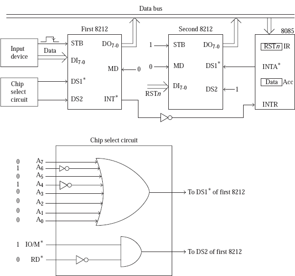
Fig.19.9 interrupting input port and RSTn supply port
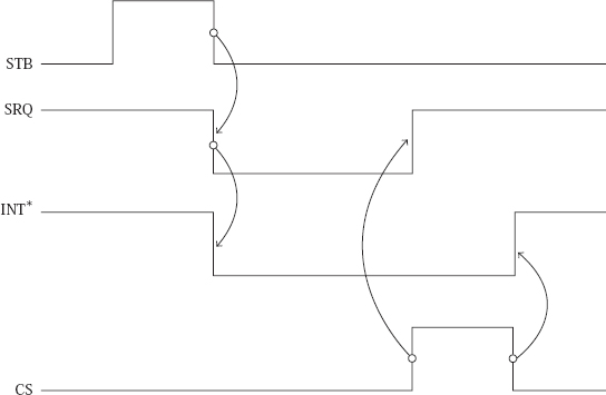
Fig.19.10 Timing diagram for INT* output
As can be verified from Fig. 19.3, high to low transition of STB causes SRQ output to make a high to low transition. High to low transition of SRQ output causes INT* to be activated. A little later, 0 to 1 transition of CS causes SRQ to go high. Finally, 1 to 0 transition of CS causes INT* to be deactivated.
In the chip select portion of Fig. 19.9, it should be noted that we should connect A7-0 and not AD7-0. Otherwise the chip will get selected wrongly when from some input port the processor reads a data value of 50H. Alternatively, if AD7-0 is not demultiplexed, we can connect A15-8 instead of A7-0, as both will have same address when IO/M* = 1.
As supplier of eight RST instructions: In 8085 we have TRAP, RST7.5, RST6.5, RST5.5, and INTR as the five interrupting pins. Suppose we have more than five I/O devices that would like to perform interrupt-driven data transfer, then on some interrupt pins more than one I/O device will have to interrupt, as shown in Fig. 19.11.
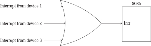
Fig. 19.11 several devices interrupting on INTR pin
In this case any of the three devices can interrupt the 8085 on INTR pin. So the 8085 does not know the origin of the interrupt request. Thus, in the ISS for INTR, which is now called ILS (interrupt level subroutine), using software the 8085 has to identify the device that needs service. It is essentially checking the interrupt status of each of the devices, till the device that needs service is identified. This process is called ‘polling’. Once the device that needs service is identified, branch should take place to the appropriate ISS. However, polling is slow and thus the interrupt response becomes slow.
This problem can be solved to a limited extent in 8085. Upto eight devices are allowed to interrupt on INTR pin and an 8212 supplies automatically a unique RSTn instruction based on the interrupting device. The interrupting device is identified by hardware in this case resulting in fast interrupt response. This mechanism is illustrated in Fig. 19.12.
Let us say we have eight devices, device 0-7, which would like to perform interrupt-driven data transfer with 8085. Let us say device 0 has the highest priority and device 7 the lowest priority. These devices send their interrupt requests to the clock inputs of eight D-type flip-flops. As can be seen from the figure, whenever a device generates an interrupt request, the Q output of the corresponding D flip-flop is reset to 0. Initially, all these flip-flop outputs are set to 1 state using the ResetOut signal of 8085. These Q outputs are connected to the eight active low inputs of a 74148 priority encoder. In this priority encoder X7 is the highest priority input and X0 is the lowest priority. As such, Q0 output is connected to X7 input. If several inputs are active simultaneously for the priority encoder, the three active low outputs on A2-0 will depend on the highest priority input that is active. Thus, if all the inputs are active, the output on A2-0 will be 000 indicating that X7 is the highest priority input that is active. The relevant truth table for 74148 is provided in Fig. 19.13.
The Q outputs of the D flip-flops are connected to a NAND gate. The output of the NAND gate is connected to INTR pin of 8085. So whenever an interrupt request is generated by an I/O device, the corresponding Q output is reset to 0 causing the 8085 to be interrupted on INTR pin. The 8085 completes the instruction that is being currently executed, and then generates INTA*.
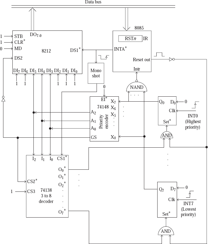
Fig.19.12 8212 as supplier of eight RSTn instructions
The INTA* output of 8085 is connected to DS1* input of an 8212. For this 8212, MD pin is connected to logic 0. STB and CLR* are connected to logic 1. DS2 is connected to GS output of 74148 after inversion. Also the data inputs DI7, DI6, DI2, DI1, and DI0 are tied to logic 1. DI5, DI4, and DI3 are connected to the A2, A1, and A0 outputs of the priority encoder. The input on DI7-0 corresponds to RSTn code, as explained in successive paragraphs. So when INTA* is activated, the 8212 sends out on Do7-0, the RSTn code present on DI7-0. Intel 8085 receives the RSTn code present on Do7-0 into the IR register. Now 8085 branches to n* 8. At this location there is a jump instruction to jump to say, location 3500H. From location 3500H onwards the ISS for INTR when device ‘n’ needs service is stored.
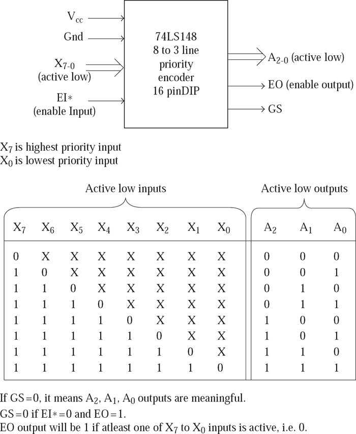
Fig. 19.13 Truth table of 74148 priority encoder
It may be noted that the code for an RST instruction is 11nnn111, where nnn can have values from 000 (for RST0) to 111 (for RST7). Thus, the data inputs of the 8212 have RSTn code depending on priority encoder output. If device 0 interrupt request occurs, the 8212 will have at its data inputs the code for RST 0. If device 4 interrupt request is currently the highest priority interrupt among the interrupt requests that are active, 8212 will receive RST4 code at its data inputs. If only device 7 interrupt request is currently active, 8212 will receive RST7 code at its data inputs.
After device n interrupts the 8085 and the 8085 branches to the appropriate ISS, the corresponding Q output of the D flip-flop should be set to 1, so that INTR becomes deactivated. This is achieved using the 74138 (3 to 8 decoder) chip. It has three active high inputs I2, I1, and I0. These are driven by A2, A1, and A0 outputs of priority encoder. It has eight active low outputs O0-7. If A2, A1, A0 = 000, then O0 of 74138 will become logic 0, which sets Q0 to 1. Similarly, if A2, A1, A0 = 111, then O7 of 74138 will become logic 0, which sets Q7 to 1. The monoshot in the figure ensures that Q output of D flip-flop is set to 1 only after 8085 has received the RSTn instruction. Connection of GS output of 74148 to CS2* input of 74138 ensures that 74138 is selected only when valid A2, A1, A0 values are output by 74148.
19.2.2 APPLICATIONS OF 8212 IN MODE 1
Following applications of 8212 in mode 1 operation will be discussed.
- As low-order address latch;
- As an interrupting output port.
Intel 8212 as low-order address latch: In 8085, low-order address lines and data lines are multiplexed and are available as AD7-0. Many times it is convenient to have address and data separated on different lines. For example, if we want to connect a chip like 2716(2K×8 EPROM) in a 8085-based system, the 2716 needs 11-bit address on its address pins, and it has separate 8 pins for data. If we connect the AD7-0 pins of 8085 to the LS 8 address pins of 2716, the address will be available for only one clock cycle in a machine cycle. Thus, demultiplexing of address and data by latching the low-order address becomes necessary. This can be achieved by using the 8212 as a latch as shown in Fig. 19.14.
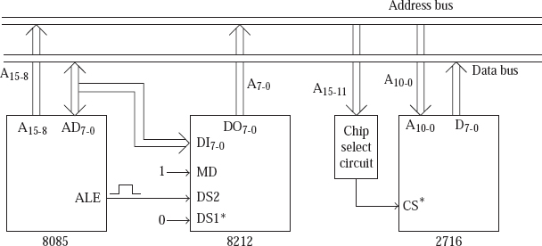
Fig.19.14 8212 as low-oeder address latch
In this case, 8212 is used in mode 1. So Do7-0 lines are always enabled. DS1* is tied to 0. DS2 is connected to the ALE output of 8085. When address is present on AD7-0, ALE signal is pulsed by 8085 during the first clock cycle T1 of any machine cycle (except BI machine cycle). This causes activation of DS2, and the address information present on DI7-0 comes out on Do7-0. After this first clock cycle in the machine cycle ALE goes to 0. This results in latching of address information in 8212. Do7-0 is always enabled in mode 1, and so the latched address information is continuously available on Do7-0 for the entire machine cycle. This is connected to the address bus.
Only during the second clock cycle T2 of a machine cycle, RD* or WR* signal is activated by 8085. By that time the information on AD7-0 will be data, and hence they are connected to the data bus of the microcomputer.
Intel 8212 as an interrupting output port: When an output device desires to perform interrupt driven data transfer with 8085, it sends a positive going pulse on STB pin of 8212, as shown in Fig. 19.15.
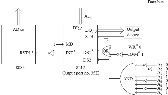
Fig. 19.15 8212 as an interrupting output port
High to low transition on STB results in activation of INT*. This results in 8085 getting interrupted on RST5.5 line as per the figure. Program control is then transferred to location 5.5 * 8. In this location we have a jump instruction to jump to say 2600H. So from 2600H the ISS for RST5.5 starts. During this ISS, OUT 35H instruction will be executed, which momentarily makes DS1* = 0 and DS2 = 1 for the 8212-causing internal CS signal to be pulsed. Then the accumulator contents enter the 8212 and is output to the output device. Also the INT* is deactivated. A little later, execution of the ISS is completed and control returns to the main program.
- Explain the function of each of the pins of 8212.
- With a neat diagram explain the working of 8212 in mode 0.
- With a neat diagram explain the working of 8212 in mode 1.
- Explain the use of 8212 as gated buffer and bi-directional bus driver.
- Explain the use of 8212 as an interrupting input port and RSTn interrupt instruction port.
- Explain the use of 8212 as a supplier of eight RST instructions.
- Explain the use of 8212 as a low-order address latch.
- Explain the use of 8212 as interrupting output port.