
24
Intel 8257—Programmable DMA Controller
![]() Concept of direct memory access (DMA)
Concept of direct memory access (DMA)
![]() Need for DMA data transfer
Need for DMA data transfer
![]() Description of 8257 DMA controller chip
Description of 8257 DMA controller chip
![]() Condition when processor is the master and 8257 is in slave mode
Condition when processor is the master and 8257 is in slave mode
![]() Condition when processor is in the HOLD state and 8257 is in master mode
Condition when processor is in the HOLD state and 8257 is in master mode
![]() Programming the 8257
Programming the 8257
![]() Address registers
Address registers
![]() Count registers
Count registers
![]() Control register (mode set register) of 8257
Control register (mode set register) of 8257
![]() Status register of 8257
Status register of 8257
![]() Description of the pins of 8257
Description of the pins of 8257
![]() Working of the 8257 DMA controller
Working of the 8257 DMA controller
![]() State diagram of 8085
State diagram of 8085
![]() Questions
Questions
This chapter deals with the programmable DMA controller—Intel 8257. It gives a detailed description of the structure and working of 8257 with neat diagrams. The various aspects of 8257 are provided under several sections as mentioned in the outline for this chapter.
 24.1 CONCEPT OF DIRECT MEMORY ACCESS (DMA)
In a microcomputer system there are basically three blocks: the microprocessor, memories such as RAM and EPROM, and I/O ports to which I/O devices are connected. Then the possible data transfers as indicated in Fig. 24.1 are as follows:
- Data transfer between microprocessor and memory (Ex. using LDA and STA instructions);
- Data transfer between microprocessor and I/O ports (Ex. using IN and OUT instructions);
- Data transfer between memory and I/O ports (DMA data transfer).
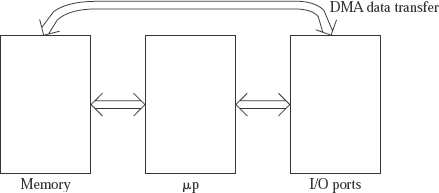
Fig. 24.1 Possible data transfers in a microcomputer system
For data transfer between microprocessor and memory or between microprocessor and I/O ports, instructions of the microprocessor are executed. As such, these data transfers are termed as programmed data transfer, which is generally used when a small amount of data transfer is involved.
Both microprocessor and memory are semiconductor chips that work at electronic speeds. Hence data transfer between microprocessor and memory is generally not a problem. In case memory is a bit slower than the microprocessor, the processor has to insert wait states. There is no problem other than this.
The I/O ports like 8255, 8212, and so on are also semiconductor chips that work at electronic speeds. However, they are used for interfacing I/O devices that are electromechanical in nature, and hence very slow compared to the speed of the microprocessor. As a result data transfer between microprocessor and I/O ports becomes more complex. In the chapter on 8255 the basic I/O, status check I/O, and the interrupt driven I/O schemes for data transfer between microprocessor and I/O ports are already discussed.
Data transfer between memory and I/O port directly (without going through the microprocessor) is called direct memory access (DMA). There are no instructions in the instruction set of the processor to perform DMA data transfer. The need for DMA data transfer and methods to perform it are discussed next.
24.2 NEED FOR DMA DATA TRANSFER
If programmed data transfer is used for reading from memory location 3456H and writing to output port number 50H, it takes 13 clocks for reading from memory location 3456H using LDA 3456H instruction and ten clocks to write to output port number 50H. Thus it takes a total of 23 clocks. If the processor is working at 3-MHz internal frequency with a clock period of 0.33 μs, it takes 7.66 μs. Similarly, for reading from input port 40H and writing to memory location 2345H, it takes 7.66 μs using programmed data transfer.
If DMA data transfer is used, reading from memory location 3456H and writing to output port number 50H requires only four clocks, which amounts to only 1.33 μs. Similarly, for reading from input port 40H and writing to memory location 2345H, it takes 1.33 μs using DMA data transfer.
Some I/O devices like the hard disk and the floppy disk are capable of performing data transfers at quite a fast rate. If we have a 1.44-MB floppy diskette rotating at 360 rpm, and has 18 sectors per track, each sector storing 512 bytes, then the data transfer rate becomes 54K bytes per second, or about 19 μs per byte. Hard disks can easily transfer data at least ten times faster. Hence it turns out to be 1.9 μs per byte. This is the situation when DMA data transfer becomes a must. In programmed data transfer, which needs about 7.66 μs per byte of data transfer, 4 bytes would have come out of the hard disk in the same time. Thus with fast I/O devices, DMA data transfer becomes a necessity.
Sometimes we may want to read from the A/D converter, say 1,000 times, and store the converted values in 1,000 memory locations. This may be needed to obtain statistics like the average, the largest, and the smallest, of the converted values. Using programmed data transfer, it takes 1,000 × 7.66 = 7,660 μs of processor time. Using DMA data transfer it takes only 1,000 × 1.33 = 1,330 μs. Thus DMA data transfer is desirable, if not essential, for data transfer between a slow I/O device (like A/D converter) and memory, if large amount of data transfer is desired.
Thus it is to be noted that when large amount of data has to be transferred between memory and I/O port, routing each byte via microprocessor becomes a time consuming operation. If the I/O port can directly access memory for data transfer, without processor intervention, it will be more efficient. Such a scheme is known as DMA data transfer.
However, as already mentioned, there are no instructions in the instruction set of a processor to perform DMA data transfer. If DMA data transfer has to take place without processor intervention, there must be a controller circuit on the I/O port that supervises DMA data transfer. Such a controller must have the following features.
- IOR, IOW, MR, and MW control signals generation capability.
- Memory address register to generate memory address for data transfer.
- Count register to indicate the number of bytes still to be transferred.
Generally I/O ports, like 8255 PPI chip, do not possess these features. Also, if more than one I/O port needs to perform DMA data transfer, then all these I/O ports need to have such controller circuitry. To solve this problem, Intel has developed programmable DMA controller chips like Intel 8257 and Intel 8237. Intel 8257 is described in this chapter.
24.3 DESCRIPTION OF 8257 DMA CONTROLLER CHIP
Intel 8257 is a 40-pin programmable IC available as a DIP package. Its physical and functional pin diagrams are indicated in Figs. 24.2 and 24.3, respectively.
The 8257 works in two modes—slave mode and the master mode. Similarly, the processor also works in two modes—active mode and the HOLD mode. The processor is normally in the active mode. In the active mode, the processor is the master of the computer system, including the 8257. Only when DMA transfer is required to be performed, the processor goes to the HOLD state and gives up control of the system bus. In such a state the processor is logically disconnected from the rest of the computer system, and the 8257 becomes the master for the rest of the computer system.
The 8257 is in the slave mode when the processor is programming the 8257, or when the processor is reading the contents of the internal registers of 8257. At this point of time the processor is in active mode, and is the master of the computer system, including the 8257.
The 8257 is in the master mode when the 8257 is actually controlling DMA data transfer. At this point of time the processor is in the HOLD state. Hence 8257 is the master of the computer system, excluding the processor, which is logically disconnected in the computer system.
The 8257 can be used to control DMA data transfer of as many as four I/O ports. For each I/O port there is a corresponding DMA channel. Each DMA channel has its DMA request (DRQ) input, and a corresponding DMA acknowledge (DACK*) output. In addition, each DMA channel has a 16-bit address register (AR), and a 16-bit count register (CR).

Fig. 24.2 Physical pin diagram of Intel 8257

fig24.3 Functional pin diagram of Intel 8257
The 8085 processor has two lines dedicated for DMA data operation. They are HOLD and HLDA (HOLD acknowledge). If an I/O port is in need of DMA service, it activates a DRQ input of the 8257, which in turn sends out HRQ (HOLD request) on HOLD input of 8085. The 8085 then completes the current machine cycle (note: not the current instruction cycle) and then goes to HOLD state. In the HOLD state the address pins, data pins, RD*, WR*, and IO/M* pins are tristated. Thus the 8085 is effectively disconnected from the rest of the system, which is made known by activating HLDA output of the 8085.
The 8057, which was so far a slave to the 8085, and was receiving commands from the 8085, now becomes the master of the computer system. Of course, it does not become the master of 8085, which is logically disconnected from the computer system. The 8257 resolves the priorities of the requesting I/O ports (if there is more than one DMA request active), and sends DACK* signal to the highestpriority I/O port needing DMA service.
24.3.1 CONDITION WHEN PROCESSOR IS THE MASTER AND 8257 IS IN SLAVE MODE
D7-0/A15-8 are used as bi-directional data lines for communication between the processor and an internal register of 8257.
A3-0 are input lines of 8257, to select an internal register of 8257 for communication with the processor.
IOR* and IOW* are input lines of 8257 so that the processor can read from or write to the internal registers of 8257.
MR*, MW*, and A7-4, which are the output pins of 8257, are tristated by 8257.
24.3.2 CONDITION WHEN PROCESSOR IS IN THE HOLD STATE AND 8257 IS IN MASTER MODE
D7-0/A15-8 are used as uni-directional address output lines for sending out MS byte of address from an AR in 8257.
A3-0 are output lines of 8257 and are used to send out the LS 4 bits of address from an AR in 8257.
A7-4 are output lines of 8257 and are used to send out the MS 4 bits of LS byte of address from an AR in 8257.
IOR*, IOW*, MR*, and MW* are output pins of 8257. If the required operation is DMA read machine cycle, MR* and IOW* signals will be activated by the 8257. The IOR* and MW* signals will be in the inactive state. If the required operation is DMA write machine cycle, IOR* and MW* signals will be activated by the 8257. The MR* and IOW* signals will be in the inactive state.
24.4 PROGRAMMING THE 8257
The programmer's view of 8257 is provided in Fig. 24.4. From the microprocessor point of view, it is an I/O port chip that is used exclusively for DMA control application. It is not used for interfacing I/O devices for the purpose of data transfer with the processor. This chip can be used to control DMA data transfer of as many as four I/O ports. For each I/O port there is a corresponding DMA channel. The chip provides all the features needed for a DMA data transfer.
24.4.1 ADDRESS REGISTERS
For each DMA channel there is an address register (AR) and a count register (CR). These registers are 16-bits wide. Thus, there are four ARs, AR3-0, each of 16 bits. Similarly there are four CRs, in addition to control and status registers. The control and status registers are separate 8-bit registers, but having the same address. The control register can only be written, and the status register can only be read by the processor.

Fig. 24.4 Programmer's view of Intel 8257
To select one of these registers, four address pins are needed. A3-0 address pins of 8257 are used for this purpose. The processor writes to an AR, CR, or control register by sending an appropriate address on A3-0 pins when chip select (CS*) and I/O write (IOW*) signals are active. The processor reads from an AR, CR, or status register by sending an appropriate address on A3-0 pins when CS* and I/O read (IOR*) signals are active.
An AR contains the address of a memory location that is used in DMA data transfer. The AR used in a DMA transfer is automatically incremented by 1 after every DMA access. As there are only eight pins for communication with the processor, the LS and MS bytes of an AR are written in two steps, starting with the LS byte. Thus, when the processor writes to an AR for the first time, the LS byte of the address register is written, and when it is written the second time, the MS byte is written.
First/last flip-flop:The 8257 contains a first/last (F/L) flip-flop which toggles after each access of an AR or CR. This flip-flop may be more appropriately called the MS/LS* (M/L*) flip-flop. The state of this flip-flop decides whether MS or LS bytes of an AR/CR is accessed.
If M/L* = 0, LS byte is accessed;
If M/L* = 1, MS byte is accessed.
This flip-flop is reset when the RESET input of 8257 is activated. It is also reset when the Control port is written by the processor. The LS and MS bytes should be accessed in succession. It is not proper, for example, to access AR0 and AR1 registers in the sequence indicated as follows.
Write to AR0; LS byte of AR0 is written
Write to AR1; MS byte of AR1 is written, when our intention was to write to LS byte of AR1
Write to AR0; LS byte of AR0 is written again, when our intention was to write to MS byte of AR0
Write to AR1; MS byte of AR1 is written again
Interrupts should be disabled prior to programming the registers of 8257. Otherwise, an interrupt could occur just after accessing the LS byte of a register and can cause problems.
24.4. COUNT REGISTERS
There are four CRs, CR3-0, each of 16 bits. When the processor accesses a CR that is 16-bits wide, the LS and MS bytes of the register are alternately accessed, starting with the LS byte. Again, the M/L* flip-flop helps in this requirement. The CR contains information about the number of bytes to be transferred using DMA. It is decremented by 1 for every byte of DMA data transfer. When the CR becomes 0, it performs the last DMA data transfer which results in the activation of the terminal count (TC) output by the 8257. There is only one TC output that is used by all the four channels. The processor reads the status port of 8257 to find out which channel was responsible for the activation of TC output by 8257.
Although a CR is 16-bits wide, only the LS14 bits of the register are used to specify the number of bytes to be transferred using DMA. So a maximum of 214 = 16K = 16,384 bytes can be programmed for data transfer. If N is the number of bytes to be transferred using DMA data transfer, we have to load (N-1) in the LS 14 bits of the CR. If the CR is loaded with 0 value in the LS 14 bits, only one byte will be transferred.
The MS 2 bits of a CR specify the type of DMA transfer. It can be DMA read (read from memory and write to I/O port), DMA write (read from I/O port and write to memory), or DMA verify. The meaning of the MS 2 bits of a CR are indicated as follows, if the 8257 is connected as I/O-mapped I/O device. In such a case, the IOR* and IOW* signals generated by the processor are connected to IOR* and IOW* input pins of 8257.

In the above case, when bit 15 is 1, the 8257 generates MR* and IOW* signals. When bit 14 is 1, it generates MW* and IOR* signals.
If desired, 8257 can be connected as a memory-mapped I/O device in a system. In such a case, the MR* and MW* signals generated by the processor are connected to IOR* and IOW* pins of 8257. The meaning of the MS 2 bits of a CR are changed as indicated in the following, if the 8257 is connected as memory-mapped I/O device.

In the above case, when bit 15 is 1, the 8257 generates IOR* and MW* signals. When bit 14 is 1, it generates IOW* and MR* signals.
In DMA verify mode, no control signal is activated by 8257. Hence actual data transfer does not take place. It is normally used after some data have been transferred to an I/O port by memory using DMA read operation. It verifies that the information transferred to the I/O port is a true copy of the data in memory. For this purpose, the 8257 sends out DACK* signal for each DMA verify cycle. The peripheral device may use these signals to verify the data it has acquired. It calculates the CRC (cyclic redundancy check) character for the stored data on I/O device and compares with the stored value of the CRC on the device to verify the data stored.
24.4.3 CONTROL REGISTER (MODE SET REGISTER) OF 8257
The processor, when active, writes to the Control register of 8257 to configure its working. To find out the status of 8257, the status register is read by the processor. The control register is 8-bits wide, and can only be written by the processor, and not read by it. It is selected when CS* = 0, A3-0 = 1000, and IOW* = 0.
The control register of 8257 is normally called the mode set register by Intel, as it sets the mode of operation of 8257. The meaning of the contents of the control register is indicated in Fig. 24.5.

Fig. 24.5 Interpretation of the contents of the control register
Enabling/disabling of DMA channels: The HRQ output of the 8257 is activated when a DRQ input is activated, and the corresponding DMA channel has been enabled. Thus, if a DMA channel is disabled, the HRQ output is not going to be activated even if the corresponding DRQ input is active. The contents of ECH3-0 bits in the control register decide the enabling or disabling of the DMA channels. After reset of 8257, all the four DMA channels are disabled.
Rotating priority: The 8257 uses fixed priority for the servicing of DMA requests after reset input of 8257 is activated. Channel 0 has the highest priority and Channel 3 has the lowest priority. Thus the priority for the channels in descending order would be 0, 1, 2, 3. In such a case, if DMA Channel 0 is enabled and the DRQ0 request is active, then the DMA channel 0 data transfer starts. If the I/O device connected to DRQ0 does not withdraw its request till all bytes are transferred, no other channel can be serviced till Channel 0 is fully serviced. Such a data transfer is called burst mode data transfer.
If all the channels are to be serviced with equal priority, the rotating priority has to be selected by setting to 1 the RTPR bit in the control register. In such a case, the DMA channel, which has just been serviced, by transferring a byte using DMA, is allotted the lowest priority. Highest priority is allocated to the channel with the next higher number. The channel numbers 0, 1, 2, 3 can be considered to form a circle. For example, if Channel 2 is serviced just then, it gets the lowest priority and Channel 3 the highest priority. Thus the priority for the channels in descending order would become 3, 0, 1, 2. Similarly, if Channel 1 is serviced just then, it gets the lowest priority and Channel 2 the highest priority. Thus the priority for the channels in descending order would become 2, 3, 0, 1. If all the four DMAs are enabled, and all the four DRQ inputs are active, then each DMA channel gets its chance to perform a DMA data transfer in four DMA cycles.
Extended write: A DMA machine cycle in which a byte is transferred directly between memory and I/O port needs four clock cycles.
- In the first clock cycle it will be in state S1. In this state, address is sent out from the relevant AR by 8257. MS byte is sent out on A15-8/D7-0 and LS byte on A7-0.
- In the second clock cycle it will be state S2. In this state, MR* (for DMA read machine cycle) or IOR* (for DMA write machine cycle) is activated.
- In the third clock cycle it will be state S3. In this state, IOW* (for DMA read machine cycle) or MW* (for DMA write machine cycle) is activated.
- In the fourth clock cycle it will be state S4. In this state, a byte of data is transferred between selected memory location and I/O port.
In the S3 state, the ready input is checked by the 8257. This ready input is similar in function to the ready input in 8085. Only if this input is a 1, the 8257 goes to state S4 during the next clock. If this input is a 0, the 8257 enters a wait state. It comes out of wait state and goes to S4 only after ready input becomes 1.
In a DMA verify machine cycle there will not be any wait states and hence it needs only four clock cycles. This is because there will not be any data transfer in a DMA verify machine cycle.
In a DMA read or write machine cycle, if the extended write bit is set, the IOW* (for DMA read machine cycle) or the MW* (for DMA write machine cycle) is generated in the second clock cycle itself. This provides for extended write times. This helps in avoiding wasteful wait states to a great extent.
Stop on terminal count (TCS bit):When the LS 14 bits of a DMA CR is decremented to zero value, the TC output of 8257 is activated. If the TCS bit in the Control register is set to 1, then the corresponding DMA channel is automatically disabled (corresponding ECH bit of control port reset to 0) on the activation of the TC output. This prevents further DMA operation on that channel. The ECH bit for the channel must be set to 1 to begin another DMA operation.
If the TCS bit in the control port is reset to 0, the activation of TC output has no effect on the DMA channel. It is then the responsibility of the I/O port to withdraw DMA request to terminate the DMA operation.
Auto load: Auto load feature is useful for repeat block operations and block chaining operations. This feature makes use of Channel 2 only, with help always from Channel 3, described as follows. Thus, in auto load mode Channel 3 is not available to the user for DMA data transfer. Hence the ECH3 bit is reset to 0 to disable Channel 3.
Repeat block operation: Assume that we want to display a page of information on the CRT. The CRT uses raster scan to display the information, which has to be refreshed about 50 times per second to get a flicker-free display of the page. The information in a page of display RAM can be sent to CRT controller using DMA read machine cycles.
Let us say, we want to transfer 1000H bytes starting from display RAM location 6000H to CRT controller. Then AR2 can be loaded with 6000H and the MS 2 bits of CR2 with 10 to signify DMA read machine cycle. The LS 14 bits of CR2 are loaded with 1000H that is 01 0000 0000 0000. Thus CR2 is loaded with 9000H. When the CRT controller activates DRQ2 input of 8257, DMA read machine cycles start. TC output is activated when CR2 contents are decremented to 8000H (when all the LS 14 bits of CR2 become 0s). At this point of time, the AR2 contents would have become 7000H.
Now it is necessary to reload AR2 with 6000H and CR2 with 9000H to repeat the sequence, and this has to be done 50 times per second to get flicker-free display. This operation is automated using the auto load feature.
If the AULD bit in the control port is set to 1, then the values stored in Channel-2 registers are automatically loaded into Channel-3 registers. Note that the auto load feature makes use of only Channel 2 with help from Channel-3 registers. Thus when AR2 and CR2 are loaded with 6000H and 9000H, AR3 and CR3 are also automatically loaded with 6000H and 9000H. When the DRQ2 request input is activated by the CRT controller, the DMA read machine cycles start. After 1000H bytes are transferred, AR2 and CR2 would have become 7000H and 8000H, and TC output would be activated. At this point of time, the Channel-2 registers are automatically reloaded from Channel-3 registers. This happens during an ‘update’ cycle, when the UD (update) flag in the status register is set to 1 by the 8257. Then the values in Channel-3 registers are copied to Channel-2 registers. The UD bit is reset to 0 by the 8257 only after DMA transfer starts again on Channel 2.
Even if the TCS bit is set to 1, it will not disable Channel 2 when TC output is activated, if AULD bit is set to 1. Hence the block operations are automatically repeated if DRQ2 input remains active.
Block chaining operation: The maximum number of bytes that can be transferred using DMA data transfer is 214=16K=16,384. What if we want to transfer the contents of memory from 6000H to 7400H, which is 17K bytes, to an I/O port? In such a situation block chaining operation can be used as described in the following.
First of all, AULD bit is set to 1, ECH2 bit to 1, and ECH3 bit is reset to 0 in the control port. Then load AR2 with 6000H and CR2 with 9000H, as described for block repeat operation. These values are automatically loaded into Channel-3 registers during a UD cycle. The UD bit in the status register is monitored till it becomes 0. Then the AR3 is loaded with 7000H and CR3 with 10 00 0100 0000 0000 = 8400H. Now the DMA transfer for Channel 2 takes place and the TC output is activated when AR2 has become 7000H and CR2 8000H. This would have transferred 1000H bytes out of our requirement of 1400H. At this point, the channel registers are reloaded from Channel-3 registers. Thus AR2 becomes 7000H and CR2 becomes 8400H. Now the next block of DMA transfer for Channel 2 results in the transfer of 400H bytes. The TC output is activated when the AR2 is 7400H and CR2 8000H. With the block chaining scheme, any amount of information can be transferred using DMA data transfer.
24.4.4 STATUS REGISTER OF 8257
The status register is 8-bits wide, and can only be read but not written by the processor. It is selected when CS* = 0, A3-0 = 1000, and IOR* = 0.
The status register of 8257 provides status information about the present state of 8257. Only the LS 5 bits are meaningful in the status register as indicated in Fig. 24.6.
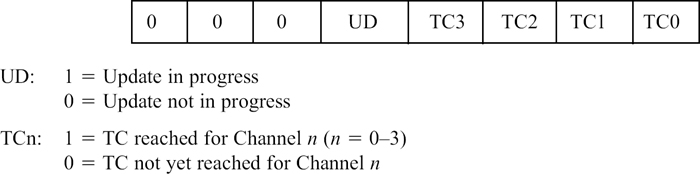
Fig. 24.6 Interpretation of the contents of the status register
The UD flag bit is not affected by a read operation of the status register. The UD flag is cleared to 0 under the following conditions.
- Intel 8257 is reset;
- Auto load feature disabled by resetting to 0 the AULD bit in the control register;
- Upon completion of UD cycle.
The TC3-0 bits are cleared to 0 under the following conditions.
- Intel 8257 is reset;
- Status register is read by the processor.
24.5 DESCRIPTION OF THE PINS OF 8257
The description of the pins of 8257 is given in Fig. 24.3. The reader is advised to read this portion once again after the programming of 8257 is explained.
Vcc and Gnd: Power supply and ground pins. 8257 uses +5V power supply.
| D7-0/A15-8: | Used as eight bi-directional data pins for communication with the processor, when the processor is active and the 8257 is in the slave mode. When the processor is in the HOLD state and the 8257 is the master, they are used to send out the MS 8 bits of memory address from an AR of 8257. | ||||||||||||||||||||||
| A3-0: | When the processor is active, they are used as address input pins of 8257 to select one of the registers inside the 8257. There are ARs, CRs, control and status registers as shown in the following table. When the processor is in the HOLD state, these pins are used to output the LS 4 bits of memory address by the 8257.
|
||||||||||||||||||||||
| A7-4: | When the processor is in the HOLD state, these pins are used to output the MS 4 bits of the LS byte of memory address by the 8257. These pins are tristated, when the processor is active. | ||||||||||||||||||||||
| RESET: | This is an active high input pin which is normally connected to the RESET OUT pin of 8085. As such, when the 8085 is reset, it sends out a logic 1 pulse on the RESET OUT pin thus resetting the 8257. After the reset of 8257, the control register contents becomes 00H. This means:
|
||||||||||||||||||||||
| DRQ3-0: | These are active high DMA request input pins, one for each of the four DMA channels. They are activated by special-purpose I/O port chips like Intel 8272—floppy disk controller, and Intel 8275—CRT controller. In fixed priority mode (when RTPR bit is 0 in the control register), DRQ0 has the highest, and DRQ3 the lowest priority. | ||||||||||||||||||||||
| DACK3-0*: | These are active low DMA acknowledgement output pins, one for each of the four DMA channels. Logical OR of chip select circuit output and DACK* output of 8257 is given as chip select input to special purpose I/O ports like Intel 8272 and Intel 8275. A DACK* output becomes 0 and then 1 for each byte of DMA data transfer. | ||||||||||||||||||||||
| IOR*: | It is an active low input pin that is activated by the processor to read an AR, CR, or the status register, when the 8257 is in the slave mode. The IOR*, generated using IO/M*, RD*, and WR* signals of 8085, is connected to this pin when 8257 is connected as I/O-mapped I/O device. If the 8257 is connected as memory-mapped I/O device, the MR*, which is generated using IO/M*, RD*, and WR* signals of 8085, is connected to this pin.
When the processor is in the HOLD state, this becomes an output pin, and is activated for a DMA write machine cycle. |
||||||||||||||||||||||
| IOW*: | It is an active low input pin that is activated by the processor to write to an AR, CR, or the control register, when the 8257 is in the slave mode. The IOW*, generated using IO/M*, RD*, and WR* signals of 8085, is connected to this pin when 8257 is connected as I/O-mapped I/O device. If the 8257 is connected as memory-mapped I/O device, the MW*, which is generated using IO/M*, RD*, and WR* signals of 8085, is connected to this pin.
When the processor is in the HOLD state, this becomes an output pin, and is activated for a DMA read machine cycle. |
||||||||||||||||||||||
| MR*: | It is an active low output pin that is in tristate when the 8257 is in the slave mode. When the processor is in the HOLD state, the 8257 drives this pin. It is activated for a DMA read machine cycle and is inactive for a DMA write machine cycle. | ||||||||||||||||||||||
| MW*: | It is an active low output pin that is in tristate when the 8257 is in the slave mode. When the processor is in the HOLD state, the 8257 drives this pin. It is activated for a DMA write machine cycle and is inactive for a DMA read machine cycle. | ||||||||||||||||||||||
| CS*: | Active low input pin used for selecting the chip. | ||||||||||||||||||||||
| Clk: | It is the clock input pin. The maximum allowed clock frequency on this input is about 3 MHz. The clock input is connected to the ClkOut pin of 8085 in an 8085-based system. | ||||||||||||||||||||||
| Ready: | This is an active high input pin. It is similar in function to the ready input of 8085. Devices with slow access times can use this input to insert wait states during DMA read or write machine cycles. The wait states are never inserted in the case of DMA verify machine cycles. | ||||||||||||||||||||||
| HRQ: | HRQ stands for HOLD request. This is an active high output pin. This is connected to the HOLD input of 8085. Whenever a DRQ input is active, and the corresponding DMA channel is enabled, the HRQ output is activated by the 8257. It then essentially requests the processor to grant control of the system bus. | ||||||||||||||||||||||
| HLDA: | HLDA stands for HOLD acknowledge. This is an active high input pin, which is connected to the HLDA output of 8085. When the HLDA input becomes active, it means that the processor has gone to HOLD state and has relinquished the system bus. Now the 8257 becomes the master in the microcomputer system. | ||||||||||||||||||||||
| TC: | TC stands for terminal count. This is an active high output pin. This output is activated when all the LS 14 bits of the CR become 0 for the DMA channel being serviced. There is a single TC output pin although there are four DMA channels. If the I/O ports connected to the DMA channels have TC input pin, then the TC output of 8257 is connected to the TC input pin of the I/O port. For example, the TC output of 8257 is connected to the TC input of Intel 8272—floppy disk controller chip. Thus when the TC output is activated, the I/O port for which DACK* is active, receives the TC input. If the TCS bit in the control port of 8257 is reset to 0, it will be the responsibility of the I/O port to withdraw the DRQ. If the TCS bit in the control port of 8257 is set to 1, the DMA channel being serviced is automatically disabled. However, if Channel 2 is being serviced, and AULD bit in the control port is set to 1, the Channel 2 remains enabled irrespective of the TCS bit value. | ||||||||||||||||||||||
| MARK: | This is an active high output pin. This output is activated when the LS 7 bits of the CR become 0 for the DMA channel being serviced. In other words, whenever the LS byte of the CR becomes 80H or 00H. This happens whenever the number of bytes still to be transferred is an integral multiple of 128 (80H). There is a single MARK output pin although there are four DMA channels. This output is not normally used in a microcomputer system, because, the chips that use DMA data transfer, like 8272 and 8275, do not have MARK input. | ||||||||||||||||||||||
| AEN: | AEN stands for address enable. This is an active high output pin. Intel 8257 outputs a 0 on AEN whenever 8085 is the master of the computer system. When the 8085 goes to the HOLD state, the 8257 outputs a 1 on AEN, indicating that 8257 is the master now. | ||||||||||||||||||||||
| ADSTB: | ADSTB stands for address strobe. This is an active high output pin which is similar in function to the ALE output of 8085. Intel 8257 outputs a 0 on this pin as long as it is in slave mode. When the 8257 becomes the master, it outputs 1 on ADSTB only during the first of the four clock cycles of a DMA machine cycle.
Fig. 24.7 illustrates the interfacing of 8257 in an 8085-based system. It uses two Intel 8212 non-programmable I/O port chips and a quad 2-to-1 multiplexer. Both 8212s are used in mode 0. At any instant of time only one of the two 8212s is selected. This is because the AEN output of the 8257 is connected to DS1* input of 8212-1 and DS2 input of 8212-2. |
Thus 8212-1 chip is selected when 8257 outputs a 0 on AEN in the slave mode. The 8212-2 chip is selected when the 8257 outputs a 1 on AEN in the master mode. It is easy to note from Fig. 24.7 that the 8085 generates the address and control signals MR*, MW*, IOR*, and IOW* when the AEN output of 8257 is 0. These control signals are generated by the 2-to-1 multiplexer using RD*, WR*, and IO/M* outputs of 8085.
MR* output is activated only when RD* is 0 and IO/M* is 0
MR* output is deactivated when RD* is 1 or IO/M* is 1
MW* output is activated only when WR* is 0 and IO/M* is 0
MW* output is deactivated when WR* is 1 or IO/M* is 1
IOR* output is activated only when RD* is 0 and IO/M* is 1
IOR* output is deactivated when RD* is 1 or IO/M* is 0
IOW* output is activated only when WR* is 0 and IO/M* is 1
IOW* output is deactivated when WR* is 1 or IO/M* is 0
Intel 8257 generates the address and control signals MR*, MW*, IOR*, and IOW* when the AEN output of 8257 is 1. These control signals are directly generated by the 8257 on its pins. The ADST output is pulsed to latch the MS byte of address sent out by the 8257.
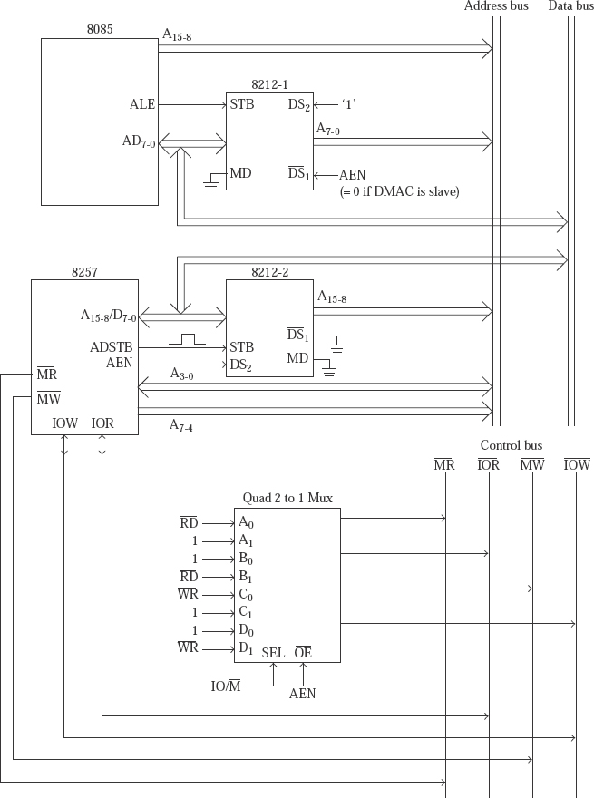
Fig. 24.7 Interfacing of 8257 in an 8085-based system
24.6 WORKING OF THE 8257 DMA CONTROLLER
First, the 8257 is programmed by the processor. At this point, the processor is the master and the 8257 works in the slave mode. The processor programs each channel by writing to the AR the starting address of memory for data transfer, and writing to the CR the number of bytes to be transferred using the DMA. The number of bytes information is specified using LS 14 bits of the CR. The MS 2 bits indicate the type of DMA data transfer. Then the processor writes to the control port (referred to as mode set register by Intel). This specifies the DMA channels that are enabled, whether it is fixed or rotating priority, and the like.
Whenever an I/O port is in need of DMA service, it activates the DRQ input of a channel. The 8257 in turn activates the HRQ. The HRQ output of 8257 is connected to the HOLD input of 8085. Thus a DMA request activates the HOLD input of 8085. The 8085 then completes the current machine cycle(not the current instruction cycle) and then goes to the HOLD state. In the HOLD state the address pins, data pins, RD*, WR*, and IO/M* pins are tristated. Thus the 8085 is effectively disconnected from the rest of the system. It announces that it is in the HOLD state by activating the HLDA output.
The 8057, which was so far a slave to the 8085, and was receiving commands from the 8085, now becomes the master of the computer system. Of course, it does not become the master of 8085, which is logically disconnected from the computer system. The 8257 resolves the priorities of the requesting I/O ports (if there is more than one DMA request active), and sends DACK* signal to the highestpriority I/O port needing DMA service. This results in chip selection of the requesting I/O device. The 8257 sends out the 16-bit memory address present in AR using the pins A15-8/D7-0, A7-4, and A3-0.
If the required operation is DMA read machine cycle, then the MR* and IOW* signals will be activated by the 8257 and the IOR* and MW* signals will be in the inactive state. If the required operation is DMA write machine cycle, then the IOR* and MW* signals will be activated by the 8257 and the MR* and IOW* signals will be in the inactive state. The outputting of memory address and the activation of control signals results in the transfer of a byte of data between the memory and I/O port directly. This DMA machine cycle takes four clock cycles. At the end of each DMA machine cycle, the CR is decremented by 1, the AR is incremented by 1, and DACK is deactivated.
There are three types of DMA data transfers:
- Single-byte transfer;
- Short-burst mode;
- Long-burst mode.
Single-byte transfer: Some I/O ports like Intel 8272 generate a DMA request for each byte of DMA data transfer. The following steps are performed for each byte of data transfer.
- Intel 8272 activates the DRQ input of 8257.
- Intel 8257 activates the HOLD input of 8085, by activating HRQ output.
- Intel 8085 enters the HOLD state, suspends program in execution, and activates the HLDA output.
- Intel 8257 activates the DACK* output.
- Intel 8257 generates the required control signals to perform data transfer of a byte. The AR is incremented and CR is decremented.
- Intel 8272 deactivates the DRQ request.
- Intel 8257 deactivates the HOLD input of 8085, by deactivating the HRQ output.
- Intel 8085 comes out of the HOLD state and deactivates the HLDA output.
- Intel 8085 resumes suspended program for some time.
- Intel 8272 reactivates the DRQ and the sequence repeated till TC is reached.
This kind of a data transfer is called Single byte transfer, as the DRQ is activated for each byte of data transfer. It is also termed Cycle stealing data transfer in the literature. This is because the 8257 steals a DMA machine cycle in the middle of an instruction cycle, when a byte of DMA is needed. This scheme is used with slow peripherals.
Short-burst mode: Some I/O ports like Intel 8275 generate a DRQ and keep it active till several bytes are transferred. The DRQ input of the 8257 is kept active depending on how the 8275 is programmed, for upto eight DACK* activations. This results in 8 bytes of DMA data transfer. Then the DRQ output remains inactive for quite some time. During this period, the HRQ output of 8257 becomes inactive resulting in 8085 coming out of HOLD state and getting into active state. Then the sequence mentioned earlier is repeated till all the bytes are transferred and the TC output is activated. This kind of a data transfer is called Short-burst mode transfer, as the DRQ input remains active till a small block of data is transferred. This scheme is used with moderately fast peripherals.
Long-burst mode: In this mode, the DRQ request is withdrawn by the I/O port only after all the bytes are transferred and the TC output is activated. But the DACK* output is pulsed for each byte of data transfer. This scheme is used with fast peripherals like hard disk controller.
24.7 STATE DIAGRAM OF 8085
By now we have fully discussed about the pins, the instruction set, and the various machine cycles of 8085. Now we study the state diagram of 8085, as illustrated in Fig. 24.8.
Intel 8085 starts in Treset state at power on. At this point the following flip-flops will have the status as shown in the following.
- Halt flip-flop reset to 0.
- The HLDA flip-flop is reset to 0. It results in the HLDA output of 8085 becoming 0.
- The INTE flip-flop is reset to 0. It disables the RST 7.5, RST 6.5, RST 5.5, and INTR.
- The INTA flip-flop is reset to 0. It results in the INTA* output of 8085 becoming 1.
The halt flip-flop is set to 1 when the 8085 decodes the instruction in IR as HLT instruction.
Intel 8085 checks the value of the HOLD input pin at the end of T2 in a machine cycle consisting of three or four clock cycles. It is checked at the end of T4 also, if the machine cycle consists of six clock cycles, like the first machine cycle of a CALL instruction. If it senses a 1 on the HOLD input, the HLDA flip-flop is set to 1. In such a case, at the end of the current machine cycle, not necessarily at the end of the instruction cycle, the 8085 activates the HLDA output and enters Thold state.
Intel 8085 checks all the interrupt request pins at the end of the last clock cycle in an instruction cycle.. If it senses any valid interrupt request the INTE flip-flop is reset to 0. This results in disabling of all interrupts except TRAP so that the ISS can be executed without further interrupts. If the 8085 has been interrupted because of INTR and none of the higher priority interrupt requests are active, then the INTA flip-flop is set to 1. This results in the activation of INTA* output of 8085.
When reset-in becomes inactive, the 8085 enters the state T1. This is the first clock cycle of a machine cycle. At the end of T1, if the HALT flip-flop status is 0, it enters state T2. At the end of T2, if the ready input of 8085 is 0 and the machine cycle is not a BI machine cycle, then the 8085 enters Twait state. (Intel 8085 executes a BI machine cycle only for DAD instruction or when it is required to respond to a vector interrupt.) As long as the ready input remains 0, the 8085 remains in Twait state. If the ready input becomes 1, then the 8085 comes out of Twait state.
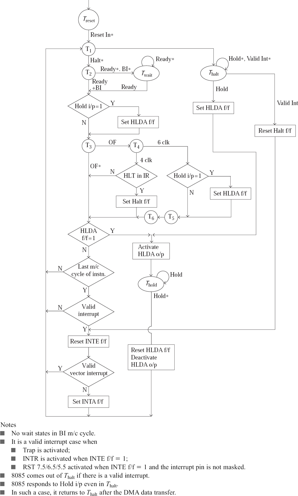
Fig. 24.8 State diagram of 8085
At the end of T2, if the ready input of 8085 is 1 or the machine cycle is a BI machine cycle, then the 8085 checks the HOLD input. If the HOLD input is not active, then the 8085 enters T3 state. If the HOLD input is active, then the 8085 sets the HLDA flip-flop, and enters the T3 state.
If it is the first machine cycle of an instruction (OF machine cycle), the 8085 enters T4 state from T3. At the end of T4, if it is the last clock cycle for the machine cycle, 8085 checks if the code for HLT instruction is in the IR. If yes, the 8085 sets the HALT flip-flop, and then checks the status of the HLDA flip-flop. If the IR is not having the code for HLT, the 8085 directly checks the status of the HLDA flip-flop.
At the end of T4, if it is a six-clock machine cycle, the 8085 again checks the HOLD input. If the HOLD input is not active, the 8085 enters T5 state. If the HOLD input is active, the 8085 sets the HLDA flip-flop, and then enters T5 state. From state T5 it enters state T6. At the end of T6 the HLDA flip-flop status is checked.
If it is not the first machine cycle of an instruction (like MR, MW, IOR, IOW, INA, BI machine cycles), the HLDA flip-flop status is checked at the end of the T3 state. Thus the HLDA flip-flop status is checked at the end of:
- T3 for MR, MW, IOR, IOW, INA, and BI machine cycles;
- T4 for OF machine cycle with four-clock cycles;
- T6 for OF machine cycle with six-clock cycles.
If the HLDA flip-flop is set, the 8085 activates the HLDA output pin and enters Thold state. It remains in the Thold state as long as the HOLD input is active. When the HOLD input is deactivated, the 8085 comes out of the HOLD state and resets the HLDA flip-flop. Then the 8085 goes ahead with the first clock cycle for the next machine cycle in the instruction by entering state T1.
If at the end of T3 (T4or T6 as the case may be) the HLDA flip-flop is in reset condition, then the 8085 finds out if it is the last machine cycle for the current instruction. If it is not the last machine cycle, the 8085 begins the next machine cycle by entering T1 state again. If it is the last machine cycle, it means the current instruction execution is complete. Then it checks for any valid interrupts. If there are no valid interrupt requests, the 8085 goes ahead with the next instruction cycle by entering T1 state again.
If there is any valid interrupt at the end of an instruction cycle, the 8085 resets the INTE flip-flop. This ensuresthat the execution of ISS can proceed without any further interrupts. Then 8085 checks to find out if INTR is the only valid interrupt. If yes, it sets the INTA flip-flop that activates INTA* output pin. Then the 8085 goes ahead with receiving a 3-byte CALL instruction, or a 1-byte RSTn instruction from an I/O device, by entering T1 state of an INA machine cycle. If an interrupt other than INTR is a valid interrupt, the 8085 directly goes ahead with BI machine cycle, by entering T1 state again.
At the end of T1, if HALT flip-flop status is 1, the 8085 enters state Thalt. If the HOLD input remains inactive and there is no valid interrupt request, the 8085 remains in Thalt state. It will wait in this state for the activation of the HOLD input or of a valid interrupt request.
If the HOLD input becomes active during Thalt, the 8085 sets the HLDA flip-flop, and activates the HLDA output pin and enters Thold state. As discussed earlier, the 8085 remains in the Thold state as long as the HOLD input is active. When the HOLD input is deactivated, it comes out of the HOLD state and resets the HLDA flip-flop. Then the 8085 re-enters Thalt state from T1 state.
If valid interrupt becomes active during Thalt, the 8085 resets the HALT, and INTE flip-flops. This ensures that the 8085 has come out of halt state, and the execution of ISS can proceed without any further interrupts. Then, as discussed earlier, the 8085 checks to find out if INTR is the only valid interrupt. If yes, it sets the INTA flip-flop that activates the INTA* output pin. Then the 8085 goes ahead with receiving a 3-byte CALL instruction, or a 1-byte RSTn instruction from an I/O device, by entering T1 state of an INA machine cycle. If an interrupt other than INTR is a valid interrupt, the 8085 directly goes ahead with BI machine cycle, by entering T1 state again.
- What is meant by DMA? What is the need for DMA data transfer?
- Describe the need for a DMA controller in a microcomputer system.
- Provide a brief overview of the working of 8257 DMA controller.
- Briefly describe the functions of the pins of 8257.
- Explain the function of A3-0, MR*, MW*, IOR*, IOW*, and D7-0/A15-8 pins of 8257 when it is working as a slave to the processor.
- Explain the function of A3-0, MR*, MW*, IOR*, IOW*, and D7-0/A15-8 pins of 8257 when it is working as a master controlling DMA data transfer.
- Describe the meaning of the MS 2 bits of a count register, when 8257 is connected as a memory-mapped I/O device.
- Describe the meaning of the MS 2 bits of a CR, when 8257 is connected as an I/O-mapped I/O device.
- Explain auto load mechanism feature of 8257.
- With a neat diagram explain the interfacing of 8257 in an 8085-based system.
- Describe the function of the important registers available in 8257.
- With an example, describe the meaning of every bit in the control port of 8257.
- With an example, describe the meaning of every bit in the status port of 8257.
- With a neat diagram describe the state transition diagram of 8085 processor.
- Write the control word needed to perform the following:
- Enable Channels 0, 3 and disable Channels 1, 2.
- Enable rotating priority and extended write, disable auto load and TC stop.
- Assume 8257 control port contains 53H. How does 8257 react to this?
- Assume 8257 status port contains 53H. What does it mean?
- Explain single byte transfer, short burst mode, and long burst mode data transfers.