
20
8255 Programmable Peripheral Interface Chip
![]() Description of 8255 PPI
Description of 8255 PPI
![]() Interface with microprocessor
Interface with microprocessor
![]() Interface with I/O devices
Interface with I/O devices
![]() Operational modes of 8255
Operational modes of 8255
![]() Control port of 8255
Control port of 8255
![]() Mode definition control word
Mode definition control word
![]() Port C bit set/reset control word
Port C bit set/reset control word
![]() Mode 1—strobed I/O
Mode 1—strobed I/O
![]() Interrupt-driven and status check data transfers
Interrupt-driven and status check data transfers
![]() Interrupt-driven input operation
Interrupt-driven input operation
![]() Interrupt-driven output operation
Interrupt-driven output operation
![]() Status check input operation
Status check input operation
![]() Status check output operation
Status check output operation
![]() Mode 2—bi-directional I/O
Mode 2—bi-directional I/O
![]() Interrupt-driven bi-directional operation
Interrupt-driven bi-directional operation
![]() Status check bi-directional operation
Status check bi-directional operation
![]() Questions
Questions
In the previous chapter non-programmable I/O port chip 8212 was discussed. However, programmable peripheral chips are more popular because their setting can be changed by the program, without recourse to change in wiring or hardware. A very popular programmable I/O port chip is the Intel 8255. This will be discussed in detail in this chapter.
 20.1 DESCRIPTION OF 8255 PPI
Intel 8255 is a programmable peripheral interface (PPI) chip. It means that it is a programmable chip used for interfacing or connecting peripheral devices. Peripheral device is another name for I/O device. Also, it is well known that I/O ports are used for connecting I/O devices. Thus, in very simple words, 8255 is a programmable I/O port chip.
The 8255 is available as a 40-pin chip in a dual in line package. Figure 20.1 illustrates the functional pin diagram of 8255. The actual pin diagram of 8255 is provided in Fig. 20.2. Figure 20.3 provides a simplified architecture of 8255. It works on a power supply of + 5 V dc. It has two programmable I/O ports each of 8 bits in size, and two programmable I/O ports each of 4 bits in size. They are called Port A, Port B, Port C upper, and Port C lower, respectively. These port pins have the ability to source 1 mA of current at 1.5 V, when programmed to work as output pins. This provides the capability of directly driving Darlington transistors for applications, such as printers and high-voltage displays.

Fig. 20.1 Functional pin diagram of 8255

Port C upper and Port C lower are addressed as if they constitute a single 8-bit port. This can be verified from Table 20.1, which indicates port selection. Thus Port C can be thought of as being divided into two portions of 4 bits each. They can be independently programmed as input or output lines. So, for example, Port C lower can be programmed as input and Port C upper can be programmed as output. However, in most applications Port C is connected to an 8-bit input device or output device. In such cases both portions of Port C are programmed for the same function.

Fig. 20.3 Simplified architecture of 8255
Table 20.1 Port selection in 8255

Also any line of Port C, which is programmed as output can be set to logic 1, or reset to logic 0 using the single bit set/reset feature of Port C also. This feature reduces software requirement in control-based applications. This facility is provided only for Port C. This feature is also used for enabling/disabling interrupts from 8255 ports, as will be discussed later.
The functionality of these three ports is decided by the contents of the control port. The control port can only be written by the microprocessor. Intel 8085 cannot read it. Thus, there are three ports which can be used for I/O operations, and a control port to control the function of these ports. A port inside the 8255 is selected for communication by the 8085 by the address-input pins A1 and A0, as shown in Table 20.1. The direction of data transfer is dictated by the RD* and WR* input signals. Of course, the 8255 chip should be first of all selected by activation of CS* signal before a port inside 8255 can be selected. For example, the control port is written with the contents sent out by 8085 on D7-0 pins of 8255 when CS* = 0, WR* = 0, A1 = 1, and A0 = 1. Thus, A1 and A0 together with RD*, WR*, and CS* decide the manner in which 8085 communicates with 8255.
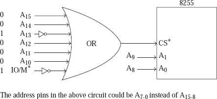
Fig. 20.4 8255 connected as I/O-mapped I/O
The 8255 can be connected in a microcomputer system as either memory-mapped I/O or I/O-mapped I/O. Suppose we want 8255 connected as I/O-mapped I/O with addresses of Port A, Port B, Port C, and control port as 20H, 21H, 22H, and 23H, respectively. Then one of the possible chip select circuits is shown in Fig. 20.4. In this figure A7-0 could have been used instead of A15-8.
Similarly, suppose we want 8255 connected as memory-mapped I/O with addresses of Port A, Port B, Port C, and control port as FFFCH, FFFDH, FFFEH, and FFFFH respectively. Then one of the possible chip select circuits is shown in Fig. 20.5. In this figure A7-0 is the LS byte of address generated using 8212 or 74LS373 as an address latch.
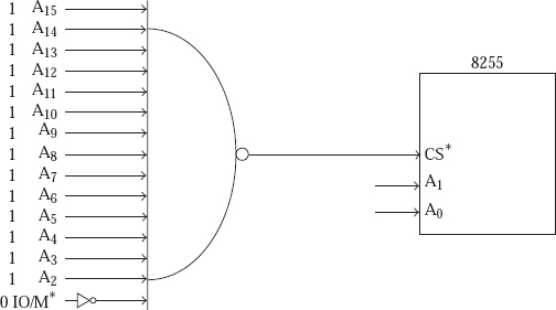
Fig. 20.5 8255 connected as memory-mapped I/O
20.1.1 INTERFACE WITH MICROPROCESSOR
The pins of 8255 that are used for interfacing with a microprocessor are described in the following:
| CS* | It is an active low input pin for 8255. If this pin is at logic 0, the 8255 chip is selected for communication with the microprocessor. If the chip is not selected the data lines D7-0 of 8255 will be in tristate. |
| D7-0 | These pins are the data pins, which are used by 8255 for communication with the microprocessor. They are connected to the data bus of the microcomputer system. |
| RD* | It is an active low input pin for 8255. It is connected to RD* output of 8085. The 8085 activates the RD* input of 8255 when it wants to read the data present in a port of 8255. |
| WR* | It is an active low input pin for 8255. It is connected to WR* output of 8085. The 8085 activates the WR* input of 8255 when it wants to write data to a port of 8255. |
| A1, A0 | These are address-input pins. They select one of the ports inside 8255 for communication with the microprocessor, as indicated in Table 20.1. |
| Reset | It is an active high input pin. It is connected to ResetOut output of 8085. It is used to reset the 8255. After a reset of 8255, all the three ports of 8255 work as input ports in mode 0, which is the simplest mode of operation. Operational modes of Ports are described later. |
20.1.2 INTERFACE WITH I/O DEVICES
The pins of 8255 that are used for interfacing with I/O devices are described in the following.
| PA7-0 | These eight pins are used by the 8255 for communicating with an I/O device. These pins are output pins if Port A is programmed as an output port. They are input pins if Port A is programmed for input operation. |
| PB7-0 | These eight pins are used by the 8255 for communicating with an I/O device. These pins are output pins if Port B is programmed as an output port. They are input pins if Port B is programmed for input operation. |
| PC7-4 | These four pins are used by the 8255 for communicating with an I/O device. These pins are output pins if Port C upper is programmed as an output port. They are input pins if Port C upper is programmed for input operation. |
| PC3-0 | These four pins are used by the 8255 for communicating with an I/O device. These pins are output pins if Port C lower is programmed as an output port. They are input pins if Port C lower is programmed for input operation. |
However, Port C pins can have other functions assigned to them in some cases as will be described next.
20.2 OPERATIONAL MODES OF 8255
Intel 8255 supports three modes of operation. They are mode 0, mode 1, and mode 2.
Mode 0 is called simple I/O or basic I/O, as it is the simplest mode of operation. All of the I/O ports in 8255 are capable of being programmed to work in mode 0. This mode is used with I/O devices whose timing characteristics are clearly known. For example, if we have an input device that wants to send to the microprocessor a byte every 0.5s, we can execute an IN instruction every 0.5s to receive the information. In this mode the port inputs are not latched. Thus, the input device must continue with the data on port pins till the port data is read by the microprocessor. So it is useful for reading switch settings, but not useful for reading from a keyboard. Similarly, if we have an output device that wants to receive from the microprocessor a byte every 0.25s, we can execute an OUT instruction every 0.25s to send the information. In this mode the port outputs are latched. Thus, the microprocessor is not required to continuously send the data to the port till the output device receives the port data. It is useful, as an example, for sending data to LED display that updates the display based on the latched output.
Mode 1 is called strobed I/O or handshake I/O. This mode is useful when, for example, an input device supplies data to the microprocessor at irregular intervals. In such a case the input device must somehow tell the input port that new data has entered the port. Then the port must inform the processor to read the data. Finally once the processor has read the data, the port must inform the input device that the processor has already read the data. These informations are provided by signals called ‘handshake signals’. It is something like the handshake between two strangers, to come to know about each other before they enter into a dialogue. A port programmed to function in mode 1 uses three handshake signals. Port C provides these handshake signals. Only Port A and Port B can work in mode 1. Port A uses three lines of Port C for handshaking purposes. Port B uses another three lines of Port C for handshaking. Remaining two lines of Port C can be used for simple I/O in mode 0. If only Port A or Port B is working in mode 1, then five lines of Port C are free for use in mode 0.
In mode 0 or mode 1, a port is required to work as an input port or as an output port. It depends on whether an input device or an output device is connected to the port. In contrast with this, mode 2 is called bi-directional handshake I/O. It is useful when the microprocessor sometimes desires to receive information, and at some other times desires to send information to the I/O device connected to 8255. An example is communication with a floppy disk controller card. As mode 2 is bi-directional handshake I/O, it needs more handshake lines than the unidirectional mode 1 strobed I/O. Thus, mode 2 operation makes use of five lines of Port C for handshaking purposes. Only Port A can work in mode 2. The remaining three lines of Port C are used for handshaking if Port B is in mode 1. However, if Port B is functioning in mode 0, these three lines of Port C are used for simple I/O.
In view of this it can be concluded that:
- Port A can work in mode 0, mode 1, or mode 2;
- Port B can work in mode 0 or mode 1;
- Port C works in mode 0 if Port A and Port B are in mode 0. Otherwise, any free lines of Port C, after allocating handshake lines, are used in mode 0.
When the 8255 is reset Port A, Port B, and Port C are initialized to work as input ports in mode 0. This is done to prevent destruction of circuitry connected to a port to which an input device is connected. If ports were initialized as output ports after reset or power-on, a port might try to output to an input device, which might destroy the port, and/or the input device. However, when ports are initialized as input ports, even if output devices are connected to the ports there cannot be any damage to the ports or the output devices.
The contents of the control port decide the 8255 configuration, that is, the way in which the 8255 is programmed to work.
20.3 CONTROL PORT OF 8255
There are two types of command words or control words in 8255. They are:
- Mode definition control word and
- Port C bit set/reset control word.
Both these are written to the control port only. From the point of view of the microprocessor there is a single 8-bit control port, which is selected when CS* = 0, WR* = 0, A1 = 1 and A0 = 1. But internally there are two control ports, one for mode definition control and another for Port C bit set/reset control. The contents of the control port get latched in mode definition control port if the MS bit of control port = 1. If the MS bit of control port = 0, the contents of the control port gets latched in Port C bit set/reset control port. This can be seen from Fig. 20.3.
20.3.1 MODE DEFINITION CONTROL WORD
Figure 20.6 explains the mode definition control word.

Fig. 20.6 Mode definition control word
Bit 7 must be 1 to indicate that the control port contains mode definition control word. Bit 2 (MB) decides the mode of operation for Port B. Whenever bit 2 = 1, port B works in mode 1 and if bit 2 = 0 port B works in mode 0. Bits 6 and 5 (MA2 and MA1) decide the mode of operation for Port A. Whenever bit 6 = 1, Port A works in mode 2. If bit 6 = 0, bit 5 (MA1) decides whether Port A works in mode 1 or mode 0. As Port C can only work in mode 0, there is no question of configuring the mode for Port C. Bits 0, 1, 3, and 4 decide whether the ports are configured as input or output. For these bits, 1 = Port is configured as input and 0 = Port is configured as output.
Thus, the meaning for the various bits of control port when it contains mode definition control word is as follows.
| Bit 0 (PClI) | 1 = Port C lower (PC3-0) as input
0 = Port C lower (PC3-0) as output |
| Bit 1 (PBI) | 1 Port B as input
0 = Port B as output |
| Bit 2 (MB) | 1 = Port B in mode 1
0 = Port B in mode 0 |
| Bit 3 (PCuI) | 1 = Port C upper (PC7-4) as input
0 = Port C upper (PC7-4) as output |
| Bit 4 (PAI) | 1 = Port A as input
0 = Port A as output |
| Bits 6, 5 | 0 0 = Port A in mode 0 |
| (MA2,MA1) | 0 1 = Port A in mode 1
1 0 = Port A in mode 2 1 1 = Port A in mode 2 |
| Bit 7 | Must be 1 to indicate that it is mode definition control. |
Example 1: Configure Port A and Port B as input ports, and Port C as an output port, assuming chip select circuit as shown in Fig. 20.4.
It is an I/O-mapped I/O connection with control port address as 23H. All the eight pins of Port C are required to be output pins. This means that Port C is not providing any handshake lines to Port A or Port B. Thus, all the three ports are required to work in mode 0. So the required mode definition control word is as follows.
1 0 0 1 0 0 1 0 = 92H
This control word is written to the control Port by executing the following two instructions.
MVI A, 92H
OUT 23H
Example 2: Configure Port A as output port, Port B as input port, Port C upper as input port and Port C lower as output port, assuming chip select circuit as shown in Fig. 20.5.
It is a memory-mapped I/O connection with control port address as FFFFH. All the eight pins of Port C are required for data transfer. This means that Port C is not providing any handshake lines to Port A or Port B. Thus, all the three ports are required to work in mode 0. So the required mode definition control word is as follows.
1 0 0 0 1 0 1 0 = 8AH
This control word is written to the control port by executing the following two instructions.
MVI A, 8AH
STA FFFFH
20.3.2 PORT C BIT SET/RESET C4 WORD
Suppose Port C lower has been configured as output port. If we want to send the data 0101 out on PC3-0 we can execute the following instructions, assuming 8255 is connected as shown in Fig. 20.4.
MVI A, xxxx0101B ; x 5 don't care (it could be 0 or 1)
OUT 22H
After a while if we want to send out logic 0 on PC0 without affecting other lines of Port C, we have to execute the following instructions.
IN 22H
ANI 11111110B
OUT 22H
Intel 8255 provides an alternative way of sending out logic 1 or 0 on any pin of Port C that is configured as an output pin. It is done using the single bit set/reset feature of Port C. This feature reduces software requirement in control-based applications. This facility is provided only for Port C. Figure 20.7 explains the Port C bit set/reset control word.

Fig. 20.7 Port C bit set/reset control word
Bit 7 must be 0 to indicate that the control port contains Port C bit set/reset control word. Bits 3, 2, and 1 select a bit of Port C that is to be set or reset. Bit 0 decides whether the selected bit of Port C is to be set or reset. Bits 6, 5, and 4 are not used in this control word. They are generally loaded with 000.
Thus, the meaning for the various bits of control port when it contains Port C bit set/reset control word is as follows.
| Bit 0 (S/R*) | 1 = Set Port C bit selected by bits 3, 2, and 1
0 = Reset Port C bit selected by bits 3, 2, and 1 |
| Bits 3, 2, 1 (SB2, 1, 0) | 000 = Select bit 0 of Port C
001 = Select bit 1 of Port C 011 = Select bit 3 of Port C 100 = Select bit 4 of Port C 101 = Select bit 5 of Port C 110 = Select bit 6 of Port C 111 = Select bit 7 of Port C |
| Bits 6, 5, 4 | Are don't cares. Generally loaded with 000 |
| Bit 7 | 0 to indicate it is Port C bit set/reset control |
Thus, to reset PC0 using the Port C bit set/reset feature we have to execute only the following two instructions.
MVI A, 0 000 000 0B
OUT 23H
Similarly, the following two instructions set PC2.
MVI A, 0 000 010 1B
OUT 23H
The main use of Port C bit set/reset control word is for enabling or disabling Port A and Port B interrupts when they work in strobed mode operation. This will be discussed later.
20.4 MODE 1—STROBED I/O
Mode 1 is called strobed I/O or handshake I/O. This mode is useful when an input device supplies data to the microprocessor at irregular intervals or an output device desires data from the microprocessor at irregular intervals. A port programmed to function in mode 1 uses three handshake signals. Port C provides these handshake signals. Only Port A and Port B can work in mode 1.
PC2, PC1, and PC0 pins provide the handshake signals for Port B when it is configured as handshake input port or output port. Similarly, PC5, PC4, and PC3 pins provide the handshake signals for Port A when it is configured as handshake input port. However, PC7, PC6, and PC3 pins provide the handshake signals for Port A when it is configured as handshake output port. Note that PC3 pin will be a handshake line for Port A in input and also output operations. If both Port A and Port B work in mode 1, the remaining two pins of Port C can be used for simple I/O in mode 0. If only Port A or Port B is working in mode 1, then five pins of Port C are free for use in mode 0.
Example 1: Configure Port A as strobed input port, Port B as strobed output port, and PC7, PC6 as output lines.
The required mode definition control word is shown in Fig. 20.8.

Fig. 20.8 Mode definition control word for Ex. 1
It is to be noted that the LS bit is a don't care. This is because all the four lines of Port C lower are used for handshaking purposes some of which will be input pins and some others outputs. The 8255 will automatically configure these handshake pins, and so it is unimportant whether this LS bit is a 0 or a 1.
Bit 3 must be a 0 to indicate that PC7 and PC6 are output lines. In this case it does not mean that the entire Port C upper is output, as PC5 and PC4 are used for handshaking purposes.
The instructions to achieve this requirement assuming the chip select circuit of Fig. 20.4 are as follows.
MVI A, B4H; Treating X as 0
OUT 23H
Example 2: Configure Port A as strobed output port, Port B as strobed input port, and PC5, PC4 as input lines.
The required mode definition control word is shown in Fig. 20.9.
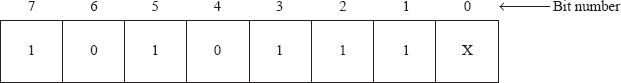
Fig. 20.9 Mode definition control word for Ex. 2
Note that bit 3 must be an 1 to indicate that PC5 and PC4 are input lines. In this case it does not mean that the entire Port C upper is input, as PC7 and PC6 are used for handshaking purposes.
The instructions to achieve this requirement assuming the chip select circuit of Fig. 20.4 are as follows.
MVI A, AFH; Treating X as 1
OUT 23H
20.4.1 INTERRUPT-DRIVEN AND STATUS CHECK DATA TRANSFERS
Among the three pins provided by Port C to a port for the purpose of handshake data transfer, one of them called INT is used for interrupting the microprocessor. Actually Port C provides INTA as interrupt from Port A and INTB as interrupt from Port B. These interrupt request outputs of 8255 can be inhibited by resetting to 0 the associated EI flip-flop or enabled by setting to 1 the associated EI flip-flop. This is accomplished by Port C bit set/reset control function. This function allows the user to allow or disallow a specific peripheral to interrupt the 8085, without altering the general interrupt structure.
For example, let us say INTB is connected to interrupt the 8085 on TRAP pin. Then whenever the TRAP pin is activated, the 8085 is always interrupted. But at some point in the program we may not want the 8085 to be interrupted from Port B. At that point even if DI instruction is executed, it cannot disable the TRAP interrupt. Other interrupts of 8085 also get disabled. But our interest may be to disable only TRAP. To solve this problem, facility is provided in 8255 to disable a Port interrupt, for example, from Port B. Then the INTB line is never activated, and so the TRAP pin is never activated.
As another example, let us say INTA is connected to interrupt the 8085 on INTR pin. Then whenever the INTR pin is activated, the 8085 is interrupted. But at some point in the program we may not want the 8085 to be interrupted from Port A. At that point if the DI instruction is executed, it will disable all the interrupts except TRAP. But our interest may be to disable only INTR. To solve this problem, facility is provided in 8255 to disable a Port interrupt, for example, from Port A. Then the INTA line is never activated, and so the INTR pin is never activated.
If Port interrupt is enabled, then the data transfer can be performed in the interrupt-driven mode. If Port interrupt is disabled, we have to resort to status check data transfer.
When Port B is programmed to work in mode 1 (input or output), if PC2 bit is set to 1, Port B EI flip-flop will be set to 1 thus enabling Port B interrupt. This can be seen from Fig. 20.3. It is to be noted that when Port B works in mode 1, PC2 pin will receive an input handshake signal. The design is such that the logic value on this pin does not enter PC2 bit. So the PC2 bit can be set or reset using Port C bit set/reset control without regard to the logic value on PC2 pin.
If Port B is working in mode 1 input and PC2 is set to 1, INTB will be activated when Port B is filled with new data by the peripheral. If PC2 bit is reset to 0, even if new data is supplied by the peripheral, INTB will not be activated.
If Port B is working in mode 1 output and PC2 bit is set to 1, INTB will be activated when the peripheral empties data from Port B. If PC2 bit is reset to 0, then even if the peripheral empties data from Port B, INTB will not be activated.
Similarly, when Port A is programmed to work in mode 1 input, if PC4 bit is set to 1, Port A interrupt is enabled. It is disabled if PC4 bit is reset to 0. Finally, when Port A is programmed to work in mode 1 output, if PC6 bit is set to 1, Port A interrupt is enabled. It is disabled if PC6 bit is reset to 0. PC4 and PC6 bits can be set or reset using Port C bit set/reset control without regard to the logic value on PC4 and PC6 pins when Port A is working in mode 1 input and mode 1 output, respectively.
It is to be noted that after a reset of 8255, Ports A and B interrupts are disabled. They are also disabled following the execution of mode definition control word.
20.4.2 INTERRUPT-DRIVEN INPUT OPERATION
Let us say we have an input device that supplies data at irregular intervals. Then we connect it to say Port B of 8255, which is configured to work in mode 1. Figure 20.10 depicts the details. Figure 20.11 provides the timing diagram for this data transfer.
It makes use of three handshake signals supplied by Port C. STB* is an input pin to 8255, and IBF and INT are output pins of 8255 as described in the following.
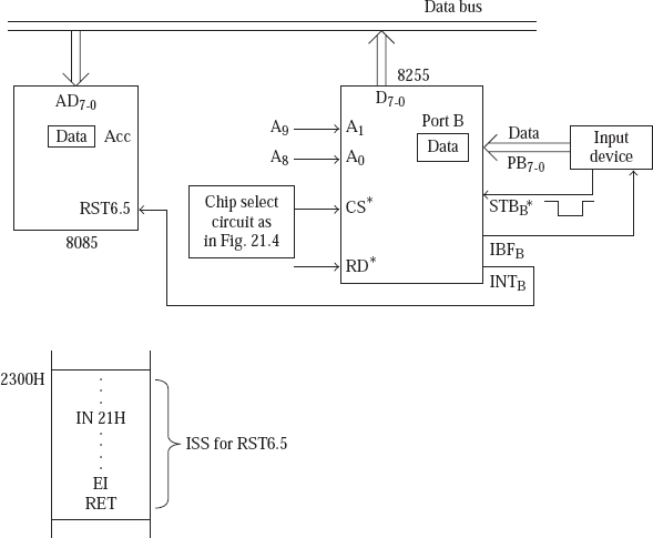

From the previous information, it should be clear that PC2, PC1, and PC0 are the handshake signals for Port B when it is configured as handshake input port. Similarly, PC5, PC4, and PC3 are the handshake signals for Port A when it is configured as handshake input port.
For the interrupt-driven input operation, the Port interrupt should be enabled. If we want Port B in mode 1 input (without bothering about other ports), we have to use mode definition control as shown in the following. The chip select circuit for 8255 is assumed to be as in Fig. 20.4.
MVI A, 1XXXX11XB; X's are don't care bits
OUT 23H
Then, to enable Port B interrupt, PC2 bit is required to be set to 1 using Port C bit set/reset control as follows.
MVI A, 0 XXX 010 1B; X's are don't care bits
OUT 23H
The interrupt-driven handshake data transfer takes place as follows. Whenever the peripheral has data to be sent to the port, it senses the IBF output of 8255. If IBF = 0, indicating that the input buffer is empty, it sends a low-going pulse on STB*. When STB* makes a 0 to 1 transition, the data on the port pins are latched by the input buffer. By this time the IBF output is activated indicating that the input buffer has become full. Also INT output becomes logic 1. In Fig. 20.10, the 8085 is interrupted on RST6.5 pin because of the INT output. It is essentially indicating to the 8085 that there is data for it to be received from 8255.
Intel 8085 finishes execution of the current instruction. Then it stores the contents of the PC on the stack top, and then it branches to memory location 6.5 × 8 = 52 = 0034H. This of course is true if interrupts are enabled, RST6.5 is unmasked, and finally RST7.5 and TRAP, which are the higher priority interrupts, are not active. At location 0034H there will be a jump instruction to say 2300H, where the actual ISS starts. In the ISS, 8085 executes IN 21H, assuming Port B address to be 21H. This results in activation of CS* and RD* inputs of 8255. Also A1 becomes 0 and A0 becomes 1 thus selecting Port B. Thus, the Port B contents are read by the 8085 in the ISS. Since the interrupting port is serviced, INT output of 8255 is deactivated. As the input buffer has been emptied by the 8085, the IBF output is also deactivated. This completes the handshake data transfer by the input device in the ISS.
20.4.3 INTERRUPT-DRIVEN OUTPUT OPERATION
Let us say we have an output device that needs data at irregular intervals. Then we connect it to say Port B of 8255, which is configured to work in mode 1. Figure 20.12 depicts the details. Figure 20.13 provides the timing diagram for this data transfer.
It makes use of three handshake signals supplied by Port C. ACK* is an input pin to 8255, and OBF* and INT are output pins of 8255 in the description that follows.
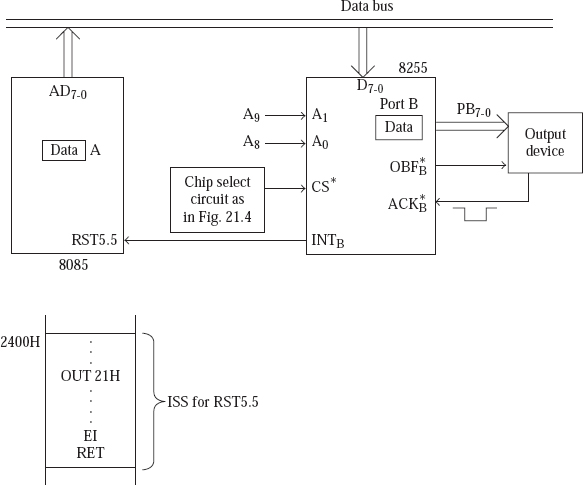
Fig. 20.12 Mode 1 output operation of 8255
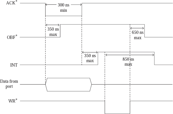
Fig. 20.13 Timing diagram for mode 1 output operation
From this it should be clear that PC2, PC1, and PC0 are the handshake signals for Port B when it is configured as handshake output port. Note that the same pins were the handshake signals in input mode also. Similarly, PC7, PC6, and PC3 are the handshake signals for Port A when it is configured as handshake output port. Note that the handshake signals for Port A differ in input and output modes except for PC3, which is INTA in both input and output modes.
For the interrupt-driven output operation, the port interrupt should be enabled. If we want Port B in mode 1 output (without bothering about other ports), we have to use mode definition control as shown in the following. The chip select circuit for 8255 is assumed to be as in Fig. 20.4.
MVI A, 1XXXX10XB; X's are don't care bits
OUT 23H
Then to enable Port B interrupt, PC2 bit is required to be set to 1 using Port C bit set/reset control as follows.
MVI A, 0 XXX 010 1B; X's are don't care bits
OUT 23H
The interrupt-driven handshake data transfer takes place as follows. Whenever the peripheral wants to receive data from the port, it senses the OBF* output of 8255. If OBF* = 0, indicating that the output buffer is full, it sends a low-going pulse on ACK*. By the time ACK* makes a 0 to 1 transition, the data in the port would have been received by the output device. By this time OBF* output is deactivated indicating that the output buffer has become empty. Also INT output becomes logic 1. In Fig. 20.12, the 8085 is interrupted on RST5.5 pin because of INT output. It is essentially indicating to the 8085 that it has to send data to the port of 8255.
Intel 8085 finishes execution of the current instruction. Then it stores the contents of the PC on the stack top, and branches to memory location 5.5 × 8 = 44 = 002CH. This of course is true if interrupts are enabled, RST5.5 is unmasked, and finally RST6.5, RST7.5, and TRAP, which are the higher priority interrupts, are not active. At location 002CH there will be a jump instruction to say 2400H, where the actual ISS starts. In the ISS the 8085 executes OUT 21H, assuming Port B address to be 21H. This results in activation of CS* and WR* inputs of 8255. Also A1 becomes 0 and A0 becomes 1 thus selecting Port B. Thus the Port B is written by the 8085 in the ISS. Since the interrupting port is serviced, INT output of 8255 is deactivated. As the output buffer has been filled by the 8085, the OBF* output is activated. This completes the handshake data transfer by the output device in the ISS.
20.4.4 STATUS CHECK INPUT OPERATION
For this type of data transfer, the Port interrupt should be disabled. If we want Port B in mode 1 input (without bothering about other ports), we have to use mode definition control as shown in the following. The chip select circuit for 8255 is assumed to be as in Fig. 20.4.
MVI A, 1XXXX11XB; X's are don't care bits
OUT 23H
Then to disable Port B interrupt, PC2 bit is required to be reset to 0 using Port C bit set/reset control as follows.
MVI A, 0 XXX 010 0B; X's are don't care bits
OUT 23H
In fact it does not matter even if these two instructions are not executed. This is because after execution of mode definition control the Port interrupts are automatically disabled.
In this type of data transfer the 8085 is not going to be interrupted by the 8255. So the 8085 has to perform a status check of 8255 to decide whether data transfer has to be performed or not. Port C provides status information about Ports Aand B when they are in handshake mode. The details are shown in Fig. 20.14.
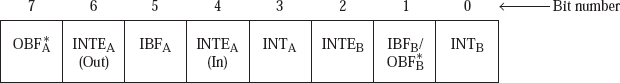
Fig. 20.14 Status information provided by Port C
Bits PC2, PC1, and PC0 provide status information about Port B when Port B works in mode 1. If Port B is working in mode 0, these bits of Port C are available for use in simple I/O. Note that bit 2 indicates EI status for Port B, and not STB* or ACK* status of Port B. Among these three status bits, the most useful one is bit 1, which provides IBFB/OBF*B information. If Port B is working in mode 1 input and if this bit = 1, it means that the Port B input buffer is full, and so 8085 is required to read data from Port B. Similarly, if Port B is working in mode 1 output and if this bit = 1, it means that the Port B output buffer is empty, and so 8085 is required to send data to Port B. Thus, whenever bit 1 of Port C is 1, the 8085 is required to perform data transfer with Port B.
Bits PC5, PC4, and PC3 provide status information about Port Awhen Port A works in mode 1 input. Then bits PC7 and PC6 are available for use in simple I/O. Note that bit 4 of Port C indicates EI status for Port A in input mode, and not STB* status of Port A. Among these three status bits, the most useful one is bit 5, which provides IBFA information. If Port A is working in mode 1 input and if this bit = 1, it means that the Port A input buffer is full, and so 8085 is required to read data from Port A.
Bits PC7, PC6, and PC3 provide status information about Port A when Port A works in mode 1 output. Then bits PC5 and PC4 are available for use in simple I/O. Note that bit 6 indicates EI status for Port A in output mode, and not ACK* status of Port A. Among these three status bits, the most useful one is bit 7, which provides OBF*A information. If Port A is working in mode 1 output and if this bit = 1, it means that the Port A output buffer is empty, and so 8085 is required to send data to Port A.
If Port A is working in mode 0, all the five MS bits of Port C are available for use in simple I/O.
The status check handshake data transfer in input mode takes place as follows. Whenever the peripheral has data to be sent to Port B, it senses the IBFB output of 8255. If IBFB = 0, indicating that the Port B input buffer is empty, it sends a low-going pulse on STB*B. When STB*B makes a 0 to 1 transition, the data on Port B pins are latched by the input buffer. By this time IBFB output is activated indicating that the input buffer has become full.
However, INTB output remains at logic 0 because Port B interrupt is disabled. Thus in this case the 8085 has to read the IBFB status of 8255 to decide whether it is required to perform data transfer with Port B or not. If the chip select circuit for 8255 is assumed to be as in Fig. 20.4, the following program segment is executed to perform status check data transfer with Port B in mode 1 input.
WAIT: IN 22H; Read Port C to check if IBFB has become 1.
      ANI 00000010B;    Reset all bits of Accumulator except bit 1
      JZ WAIT;          If IBFB = 0 then wait till it becomes 1
      IN 21H;           Now read from Port B
20.4.5 STATUS CHECK OUTPUT OPERATION
For this type of data transfer, the Port interrupt should be disabled. If we want Port A in mode 1 output (without bothering about other ports), we have to use mode definition control as shown in the following. The chip select circuit for 8255 is assumed to be as in Fig. 20.4.
MVI A, 1010XXXXB; X's are don't care bits
OUT 23H
Then to disable Port A interrupt, PC6 bit is required to be reset to 0 using Port C bit set/reset control as follows.
MVI A, 0 XXX 110 0B; X's are don't care bits
OUT 23H
In fact it does not matter even if these two instructions are not executed. This is because after execution of mode definition control the Port interrupts are automatically disabled.
The status check handshake data transfer in output mode takes place as follows. Whenever the peripheral desires to receive data from Port A, it senses the OBF*A output of 8255. If OBF*A = 0, indicating that the output buffer is full, it sends a low-going pulse on ACK*A. By the time ACK*A makes a 0 to 1 transition, the data in the port would have been received by the output device. By this time OBF*A output is deactivated indicating that the output buffer has become empty.
However, INTA output remains at logic 0 because Port A interrupt is disabled. Thus in this case the 8085 has to read the OBF*A status of 8255 to decide whether it is required to perform data transfer with Port A or not. If the chip select circuit for 8255 is assumed to be as in Fig. 20.5, the following program segment is executed to perform status check data transfer with Port A in mode 1 output. The data to be sent to Port A is assumed to be at location DATA.
WAIT: IN 22H; Read Port C to check if OBF*A has become 1
ANI 10000000B ; Reset all bits of Accumulator except bit 7
JZ WAIT; If OBF*A = 0 then wait till it becomes 1
LDA DATA
OUT 21H; Now send new data to Port A
20.5 MODE 2—BI-DIRECTIONAL I/O
In mode 0 or mode 1, a port is required to work as an input port or as an output port. It depends on whether an input device or an output device is connected to the port. In contrast with this, mode 2 is called bi-directional handshake I/O. It is useful when the microprocessor sometimes desires to receive information, and at some other times desires to send information to the I/O device connected to 8255. An example is communication with a floppy disk controller card. As mode 2 is bi-directional handshake I/O, it needs more handshake lines than the uni-directional mode 1 strobed I/O. Thus, mode 2 operation makes use of five lines of Port C for handshaking purposes. These five lines of Port C are PC7 to PC3. For the purpose of input operation, PC5, PC4, and PC3 pins provide the handshake signals for Port A when it is configured as mode 2. For the purpose of output operation, PC7, PC6, and PC3 pins provide the handshake signals for Port A when it is configured as mode 2. Note that PC3 pin will be a handshake line for Port A in mode 2 for input as well as output operations. Only Port A can work in mode 2. The remaining three lines of Port C are used for handshaking if Port B is in mode 1. However, if Port B is functioning in mode 0, these three lines of Port C are used for simple I/O.
Example 1: Configure Port A as bi-directional I/O port, Port B as basic input port, and PC2-0 as output lines.
The required mode definition control word is shown in Fig. 20.15.
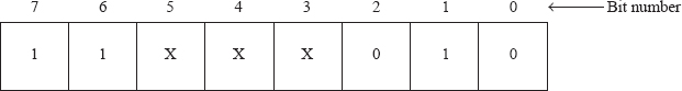
Fig. 20.15 Mode definition control word for Ex. 1
Bit 0 must be a 0 to indicate that PC2-0 are output lines. In this case it does not mean that the entire Port C lower is output, as PC3 is used for handshaking purposes.
It is to be noted that the bit 3 is a don't care. This is because all the four lines of Port C upper are used for handshaking purposes some of which will be input pins and some others will be outputs. The 8255 will automatically configure these handshake pins, and so it is unimportant whether bit 3 is a 0 or 1.
Bit 4 is a don't care because Port A is required to work in bi-directional mode. The instructions to achieve this requirement assuming the chip select circuit of Fig. 20.4 are as follows.
MVI A, C2H; Treating X as 0
OUT 23H
Example 2: Configure Port A as bi-directional I/O port, and Port B as strobed input port. The required mode definition control word is shown in Fig. 20.16.
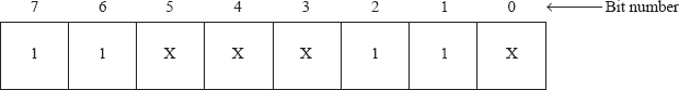
Fig. 20.16 Mode definition control word for Ex. 2
Note that bits 0 and 3 are don't cares. This is because all the eight lines of Port C are used for handshaking purposes. The instructions to achieve this requirement assuming the chip select circuit of Fig. 20.4 are as follows.
MVI A, FFH; Treating X as 1
OUT 23H
20.5.1 INTERRUPT-DRIVEN BI-DIRECTIONAL OPERATION
Let us say we have an I/O device, which supplies/receives data at irregular intervals. Then we connect it to Port A of 8255 that is configured to work in mode 2.
If we want Port A in mode 2 (without bothering about other ports), we have to use mode definition control as follows. The chip select circuit for 8255 is assumed to be as in Fig. 20.4.
MVI A, 11XXXXXXB; X's are don't care bits
OUT 23H
Then to enable Port A interrupt for input operation, PC4 bit is required to be set to 1 using Port C bit set/reset control as follows.
MVI A, 0 XXX 100 1B; X's are don't care bits
 OUT 23H
The interrupt-driven handshake data transfer from Port A to 8085 takes place as was explained earlier for mode 1 interrupt-driven input operation.
Similarly, to enable Port A interrupt for output operation, PC6 bit is required to be set to 1 using Port C bit set/reset control as follows.
MVI A, 0 XXX 110 1B; X's are don't care bits
OUT 23H
The interrupt-driven handshake data transfer from 8085 to Port A takes place as was explained earlier for mode 1 interrupt-driven output operation.
20.5.2 STATUS CHECK BI-DIRECTIONAL OPERATION
First of all to configure Port A in mode 2 (without bothering about other ports), we have to use mode definition control as shown below. The chip select circuit for 8255 is assumed to be as in Fig. 20.4.
MVI A, 11XXXXXXB; x' s are don't care bits
OUT 23H
For this type of data transfer, Port A interrupt should be disabled. To disable Port A interrupt for input operation, PC4 bit is required to be reset to 0 using Port C bit set/reset control as follows.
MVI A, 0 XXX 100 0B; X's are don't care bits
OUT 23H
Similarly, to disable Port A interrupt for output operation, PC6 bit is required to be reset to 0 using Port C bit set/reset control as follows.
MVI A, 0 XXX 110 0B; X's are don't care bits
OUT 23H
In this type of data transfer, the 8085 is not going to be interrupted by the 8255. So the 8085 has to perform a status check of 8255 to decide whether data transfer has to be performed or not.
Bits PC5, PC4, and PC3 provide status information about Port A in mode 2 input operation. Among these three status bits, the most useful one is bit 5, which provides IBFA information. If this bit = 1, it means that the Port A input buffer is full, and so 8085 is required to read data from Port A.
Bits PC7, PC6, and PC3 provide status information about Port Ain mode 2 output operation. Among these three status bits, the most useful one is bit 7, which provides OBF*A information. If this bit = 1, it means that the Port A output buffer is empty, and so 8085 is required to send data to Port A.
The status check handshake data transfer in mode 2 input is performed as was explained earlier for mode 1 handshake input operation. Similarly, the status check handshake data transfer in mode 2 output is performed as was explained earlier for mode 1 handshake output operation.
- With a neat diagram explain the functional pin diagram of 8255.
- With a neat diagram explain the internal architecture of 8255.
- Provide a chip select circuit for 8255 so that the port addresses are in the range 48H-4BH using I/O mapped I/O
- Provide a chip select circuit for 8255 so that the port addresses are in the range 2048H-204BH using memory mapped I/O.
- Explain mode 0, mode 1, and mode 2 operations of 8255 ports.
- Explain mode definition control word of 8255. Write the required mode definition control word for each of the following cases.
- Explain Port C bit set/reset control word of 8255. Write the required Port C bit set/reset -control word for each of the following cases.
- To reset to 0 bit 5 of Port C
- To set to 1 bit 3 of Port C
- With a neat diagram explain the data transfer from Port B of 8255 to 8085 in interrupt-driven mode.
- With a neat diagram explain the data transfer from 8085 to Port A of 8255 in status check mode.