4
Fundamentals of Microprocessor
![]() History of microprocessors
History of microprocessors
![]() Description of 8085 pins
Description of 8085 pins
![]() Vcc, and Vss pins
Vcc, and Vss pins
![]() AD7-0 pins
AD7-0 pins
![]() A15-8 pins
A15-8 pins
![]() ALE pin
ALE pin
![]() IO/M* pin
IO/M* pin
![]() Programmer's view of 8085: Need for registers
Programmer's view of 8085: Need for registers
![]() Meaning of programmer's view
Meaning of programmer's view
![]() Accumulator or register A
Accumulator or register A
![]() Registers B, C, D, E, H, and L
Registers B, C, D, E, H, and L
![]() Questions
Questions
 4.1 HISTORY OF MICROPROCESSORS
The history of microprocessors dates back to only the year 1971! By this time, the integrated circuits technology was so much developed that it was possible to integrate on a single chip the logic of control unit and ALU. Intel Corporation in the USA announced the first microprocessor in 1971. It was the Intel 4004. It was a 4-bit processor intended for making programmable calculators.
A 4-bit microprocessor receives 4 bits of information from outside the microprocessor, performs the necessary processing on it, and then sends out of the microprocessor a 4-bit result. It will have an ALU that can perform operations on 4-bit numbers. It is said that a 4-bit microprocessor has a word size of 4 bits.
With only 4 bits as the word size, the 4004 could only represent signed numbers in the range -8 to +7, which is indeed very small. Hence, it was not really of practical use for arithmetic calculations. However, it found applications in controlling devices. For example, it could be used to switch on or switch off a motor. This was achieved by sending out logic 1 or logic 0 from the microprocessor, and making use of a suitable driver circuitry.
Similarly, it could be used for checking if the temperature of a water bath is above or below a certain desired temperature. This was done by the reading of the logic 1 or 0 value that was developed by a temperature sensor after proper signal conditioning. The microprocessor can receive this information on a single pin to check the temperature.
Next in the evolution was the Intel 8008, the first 8-bit microprocessor. This was in the year 1972. This was soon followed by Intel 8080, also an 8-bit microprocessor. Intel 8080 was the first commercially popular 8bit microprocessor. With 8bits as the word size, it could represent signed numbers in the range of −128 to +127. This is also not a good enough range for performing arithmetic calculations. Thus, the 8080 also was used only for control applications.
By this time, some other manufacturers of integrated circuits who were till then manufacturing only components like logic gates, flip flops, shift registers, etc. got fascinated by this new product, and they also released to the market their designs of microprocessor. Notable among them was the 6800 from Motorola and Z-80 from Zilog.
The 6800 design was based on the popular PDP-11 minicomputer of those days. This chip became quite popular for control applications. Z-80 was basically an improvement over the 8080, with a large number of new and powerful instructions. This chip also became very popular in the field of control applications.
In the meanwhile, Intel came out with their improvement over the 8080. This was the Intel 8085. This was only a hardware improvement over 8080. As far as instruction set was concerned, there was basically no improvement. However, the 8085 also became very popular. The 6800, Z-80, and 8085 are all only 8-bit microprocessors, and they rule the 8-bit microprocessor world in control applications.
Around the year 1974, Intel released Intel 8048 family, their first microcontroller family. This was later followed by the Intel 8051 series of microcontrollers. Still later Intel released 8096 family of microcontrollers. In the present-day world, a large number of microcontrollers are being used in a variety of consumer products.
Around 1978, Intel released 8086, the first 16-bit microprocessor. With 16-bit word size, it was possible to represent signed numbers in the range of −32,768 to +32,767, which is quite a decent range for performing arithmetic calculations. As such, this processor became very popular not only for control applications, but also for number crunching operations. Not to be outdone, Motorola came out with 68000, their 16-bit processor. Zilog released Z-8000, again a 16-bit processor. These are the most popular 16-bit processors.
Then IBM Corporation released the first personal computer (IBM-PC) using 8088 as the CPU developed by Intel. The Intel 8088 has the same instruction set as the 8086. However, it can only receive 8bits at a time from outside, and send out 8bits at a time. Internally it is capable of performing 16-bit arithmetic. This chip was designed to make use of the processing power of a 16-bit ALU, while being capable of communicating with the common 8 bit peripheral devices of those days. The IBM-PC became extremely popular, and has now pervaded all walks of our lives. IBM released IBM-PC/XT a little later, using the same Intel 8088. This computer had a hard disk drive in addition to the floppy drives of the earlier PC.
From then on, the development of newer and more powerful processors has been very swift. Intel released 80186, which was mainly used in embedded applications. Then Intel released 80286, which was used in IBM-PC/AT. The processor could be used in multi-user, multi-tasking environment. However, the 80186 and 80286 were still 16-bit processors. In the meanwhile Motorola released 68010, also a 16-bit processor. Around this time Zilog lost the race to capture a major share in the market, with Intel and Motorola emerging as the forerunners to the top spot.
In the early 80s, Intel released the 32-bit processor, the Intel 80386. With 32-bit word size, it was possible to represent signed numbers in the range ±2×10⁹, which is quite a large range for performing arithmetic calculations. If floating point notation is used, it can represent much larger numbers. As such, this processor became very popular as the CPU in computers for number crunching operations. Not to be outdone, Motorola came out with 68020, their 32-bit processor. Intel released 80486, which was basically a 80386 processor and 80387 numeric co-processor on a single chip. Motorola released 68030. In the early 90s Intel deviated from their naming tradition and released 80586 by the name Pentium processor. It is extremely fast in performing arithmetic calculations and executing instructions. The Pentium 4 released in 2000 has 42 Million transistors worked with a clock frequency of 1.5 GHz and is rated for 1500 MIPS (Million instructions per second)
To conclude, the present-day computers based on microprocessors are already faster than the mini computers and sometimes the main frame computers of yesteryear, and they are available at a small fraction of the cost of such main frame computers. We can hope to see the release of still more powerful and at the same time cheaper microprocessors and microcontrollers in the future.
In this book, Intel 8085 processor will be discussed at great length. Armed with that knowledge, Zilog Z-80, Motorola 6800 processors, and Intel 8051 microcontroller will be discussed quite exhaustively in a few chapters.
4.2 DESCRIPTION OF 8085 PINS
Intel 8085 is fabricated as a 40-pin DIP IC. DIP stands for ‘dual inline package’. It means the package will have pins on only two sides, 20 on each side in this case.
Intel manufactures 8085 in several versions, like 8085A, 8085AH, 8085AH-2, and 8085AH-1. The 8085A is fabricated using NMOS technology. It is a variant of MOS (metal oxide semiconductor) technology. It uses n channel silicon-gate process. The AH series are more expensive processors, which use high-density MOS (HMOS) for fabrication. They typically consume 20% less power compared to the A series. The recommended internal clock frequency for the various types of 8085 is as follows.
| Type | Recommended clock frequency |
| 8085A and 8085AH | 3 MHz |
| 8085AH-2 | 5 MHz |
| 8085AH-1 | 6 MHz |
Basically they are same, the only difference being in the speed of operation, or the technology used for fabrication. In this discussion, they are simply referred to as 8085. The pin diagram of 8085 is as shown in fig. 4.1.
In fig. 4.1, the pin number and its associated function is indicated for each of the 40 pins. For example, the diagram indicates that pin number 20 is the Vss pin, which should be connected to ground, and 40 is the Vcc pin, which should be connected to +5 V dc supply. A user definitely needs this information, when he is required to wire up a microprocessor in his circuit. However, for the purpose of understanding the working of the processor, only the function of the various pins need to be known. There is no need to know which pin number performs what function. For example, to understand the working of 8085 microprocessor, the user should be aware that it needs a power supply of +5 V dc and ground. It is not necessary to know the pin numbers to which +5 V dc and ground are to be connected. A simplified diagram that does not indicate the pin numbers, but only indicates the function of the various pins, can be called a functional pin diagram. Fig. 4.2 partly provides the functional pin diagram of 8085. It shows only 22 pins. The remaining portion is explained later in the text.
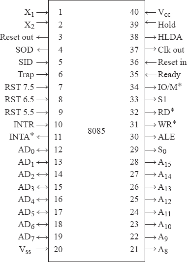

Fig. 4.2 Functional pin diagram of 8085 (incomplete)
4.2.1 VCC AND VSS PINS
Any IC needs a power supply for its working. Similarly, 8085 needs a power supply of +5 V dc for its working. Pin 40 of 8085 is the Vcc pin. It should be connected to +5 V dc power supply. Pin 20 of 8085 is the Vss pin. It should be connected to power supply ground.
4.2.2 AD7-0 PINS
Intel 8085 communicates with the outside world with 8 bits at a time. When the 8085 desires to receive 8-bit information, it receives it on the eight pins AD7, AD6, …, AD0. These eight pins are collectively called AD7-0. Their pin numbers are +9, +8, …, +2, respectively. When the 8085 desires to send out 8-bit information, it sends it out on these same pins.
Thus, these pins are used for receiving as well as sending out information. In other words, they are bi-directional pins. These pins are used for:
- Receiving the program code from memory 8 bits at a time.
- Receiving a data byte (byte = 8bits) from an input port or from memory.
- Sending out a byte to an output port or to memory
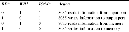
How can the same lines be used for receiving information as well as sending out information? This is not at all a problem, because at any instant of time, the processor is either receiving or sending out information, but not both. They are decided by the signals sent out on RD* and WR* pins, which are discussed next.
RD* and WR* Pins : RD*stands for ‘Read*’. A ‘*’ in this book after a signal name indicates that the signal is an active low output. Thus RD* is an active low output signal. Another popular convention is to denote RD* as ![]() .
.
RD* is pin number 32 of 8085. When the control unit in the 8085 sends out logic 0 on this pin, it is indicating that it desires to read information. Then the information comes to the processor on the AD7-0 pins. In other words, when RD* = 0, AD7-0 pins are input pins. When RD* = 1, the 8085 is not interested in reading information.
WR* stands for ‘Write*’. WR* is an active low output signal. WR* is pin number 31 of 8085. When the control unit in the 8085 sends out logic 0 on this pin, it is indicating that it desires to write information. Then the information is sent out by the processor on the AD7-0 pins. In other words, when WR* = 0, AD7-0 pins are output pins. When WR* = 1, the 8085 is not interested in writing or sending out information.
Thus the action performed by the 8085 for various combinations of RD* and WR* are as follows.

If the control unit in the 8085 sends out logic 1 on both RD* and WR* simultaneously, it means that the 8085 is not interested in reading or writing at that moment. As an example, when the 8085 is busy with some internal processing it sends out logic 1 on both RD* and WR*.
The control unit will never send out logic 0 on both RD* and WR* simultaneously. If such a thing ever happens, it means the processor has gone crazy, and you better throw it!
4.2.3 A15-8 PINS
In memory, the program to be executed is stored. It may occupy a number of locations, depending on the complexity of the program. Each location in memory is used for storing 8bits of information. There is no point in a memory location having 4 bits or 16 bits, when the 8085 can read or write 8 bits at a time. Also, memory is used for storing data and results, 8 bits in each memory location.
But, it is very inconvenient to indicate memory contents using 8bits, which is too long. Thus, memory contents are indicated in a shorter form. Suppose, the contents of the first three memory locations in binary are 0011 0101, 1010 0010, and 0001 1101. The same contents in decimal could be written as 53, 162, and 29. But converting binary number to decimal and vice versa is quite complex. Thus, it is preferred to indicate the same contents in hexadecimal notation as 35H, A2H, and 1DH.
Converting a value in binary to hexadecimal and vice versa is extremely simple. The binary number should just be written in groups of 4 bits, and convert each group of 4 bits into equivalent hexadecimal number. A hexadecimal number is many times called a ‘hex’ number for short. In this book, the content of a memory location is generally shown in hex for convenience. But, the reader should always remember that a memory location contains 8 bits of information.
When there are a number of memory locations, each location should have a unique address to identify the location. In a microcomputer, even the address has to be specified using only 0s and 1s.
If there are only two memory locations, just 1 bit address is enough to specify the location of interest. If address is 0, location 0 is selected. If address is 1, location 1 is selected.
If there are four memory locations, 2-bit address is needed to specify the location of interest. If address is 00, location 0 is selected. If address is 01, location 1 is selected. If address is 10, location 2 is selected. If address is 11, location 3 is selected.
Similarly, if there are eight memory locations, 3-bit address is needed to specify the location of interest. If address is 000, location 0 is selected, etc. and if address is 111, location 7 is selected.
Thus in general, if there are n address bits, it is possible to specify any memory location out of 2n memory locations. Intel 8085 is provided with 16 pins for sending out address information. They are
A15-8 and AD7-0 pins. On A15-8 the 8085 sends out the MS byte of address. Their pin numbers are 28 to 21, respectively. The A in A15-8 stands for ‘Address’. On AD7-0 the LS byte of address is sent out. With 16 address pins the 8085 is capable of addressing any memory location out of 216 = 26×210 = 64×1024 = 65,536 locations. In computer jargon, it is termed 64K locations, where 1K = 210 = 1024.
The addresses of these 65,536 locations in binary number system will be as follows.
0000 0000 0000 0000
0000 0000 0000 0001
0000 0000 0000 0010
.
.
.
1111 1111 1111 1111
The processor sends out the address in binary as shown previously. But, it is very inconvenient to write down addresses using 16 bits, which is too long. Thus, it is preferable to write down address in a shorter form. The same addresses in decimal could be written as 0, 1, 2, …, 65,535. But converting a binary address to decimal and vice versa is quite complex. Thus, it is preferred to write down the same addresses in hexadecimal notation as 0000H, 0001H, 0002H, …, FFFFH. In this book, the addresses are generally shown in hex for convenience. But, the reader should always remember that the processor sends out the address in binary on the 16 pins A15-8 and AD7-0.
Thus memory in a 8085-based microcomputer may be conceptualized as shown in Fig. 4.3.
If the processor is interested in reading information from memory location whose address in hex is 0002H, it sends out 00H on A15-8 and 02H on AD7-0. Then the processor sends out RD* as logic 0 and WR* as logic 1. This results in 1DH, the contents of location 0002H, coming to the processor from memory on AD7-0.
Similarly, if the processor is interested in writing the information 89H to memory location whose address in hex is 4567H, it sends out 45H on A15-8 and 67H on AD7-0. A little later, the processor sends out 89H on AD7-0 with RD* as logic 1 and WR* as logic 0. This results in 89H getting written to the location 4567H.
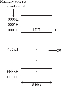
Fig. 4.3 Memory in 8085-based microcomputer
Thus, it is seen that AD7-0 is used for sending out LS byte of address, as well as sending or receiving 8bits of data. In fact, AD in AD7-0 stands for ‘address data’. This multiplexing of LS byte of address and data has been done in 8085 to save on the number of pins required for the chip.
4.2.4 ALE PIN
If LS byte of address and data are multiplexed on AD7-0, how to know whether information on AD7-0 is address or data? This is solved by the ALE signal sent out by the 8085. ALE stands for ‘address latch enable’.
At this moment, it is enough to understand that if this signal is at logic 1, 8085 is sending out address information on AD7-0. In other words, when ALE = 1, AD7-0 pins act like address pins A7-0. If ALE is at logic 0, the 8085 is sending out or receiving information. In other words, when ALE = 0, AD7-0 pins act like data pins D7-0.
Information is received on AD7-0 when ALE = 0, if RD* = 0 and WR* = 1. Then AD7-0 pins act like the input pins D7-0. Information is sent out on AD7-0 when ALE = 0, if WR* = 0 and RD* = 1. Then AD7-0 pins act like the output pins D7-0.
4.2.5 IO/M* PIN
It has already been seen that the microprocessor does not directly communicate with an I/O device. It only communicates with I/O ports. As we can have a number of I/O devices in a microcomputer system, we need to have a number of I/O ports in the system. If there are a number of I/O ports in the system, each port must have a unique address, just like each memory location has a unique address. The 8085 sends out the port address on A15-8 and AD7-0 only, just like sending out a memory address. Then, how to identify whether the address is for memory or for an I/O port? This is solved by the output signal IO/M*.
IO/M* stands for ‘input-output/memory*’. When IO/M* is logic 0, it means that the address sent out by the processor is for addressing a memory location. When IO/M* is logic 1, it means that the address sent out by the processor is for addressing an I/O port.
When IO/M* is at logic 1, how to identify whether the address is for an input port or an output port? It is addressing an input port if RD* is at logic 0 and WR* is at logic 1. It is addressing an output port if WR* is at logic 0 and RD* is at logic 1.
To conclude, the action performed by the 8085 for various combinations of RD*, WR*, and IO/M* are as follows.
So far, 22 pins of 8085 are explained. The remaining pins are explained in later chapters.
4.3 PROGRAMMER'S VIEW OF 8085: NEED FOR REGISTERS
We have seen that 8085 receives 8-bit information on AD7-0 from memory or an input port. When it comes inside the microprocessor, where does it reside inside the processor? For this purpose, there is what is called ‘register’ to store such information inside. A register is nothing but a group of flip-flops, where each flip-flop can store a bit of information. The size of such a register in 8085 has to be 8bits, to store 8bits of information.
It is necessary to have atleast one such register in any brand of microprocessor. The advantages of a register over a memory location are as follows.
- The contents of a register can be accessed much faster by the microprocessor, compared with the contents of a memory location (by ‘access’ we mean ‘read or write’).
- Instructions involving register operands will be shorter in length and are executed faster compared with instructions involving memory operands.
However, the disadvantages of a register over a memory location are as follows.
- During an interrupt service subroutine (ISS), the register values will have to be stored in an area of memory called stack. Upon return from the ISS, the register values have to be restored from the stack. This takes away the speed advantage that was mentioned earlier.
- If there are too many registers, they occupy lot of real estate on the chip, thus reducing the real estate available for the control unit and ALU.
- In instructions involving register operands, the number of bits that are free to specify the operation become reduced, thereby reducing the number of possible instructions.
The reader will be in a position to appreciate these advantages and disadvantages much better after a study of a few of the successive chapters.
In view of the earlier discussion, most microprocessors provide only a few registers on the chip. The registers provided on 8085 are A, B, C, D, E, H, and L. These are the general-purpose registers (GPRs). In addition to these registers there are a few special purpose registers (SPRs). These are discussed later.
4.3.1 MEANING OF PROGRAMMER'S VIEW
A programmer just writes a program and executes it to solve a problem. He is not bothered to know the pins of a processor, or its internal architectural details. To write a program, he needs to know only a little about the processor. For example, he needs to know the registers that are available to the programmer, and the instructions the processor understands to write his program. Thus the programmer's view of a processor, is the simplest description of the processor, without going through many details. It is similar to the driver's view of a car. From a driver's viewpoint there are only a few parts in a car, like steering wheel, brake pedal, etc. He need not even know that there should be an engine! He can still drive a car with so much of ignorance! But in reality a car will have probably a thousand parts or more.
In this chapter, the programmer's view of 8085 is discussed. To keep it simple, the complete programmer's view is not discussed. From the programmer's view, 8085 just consists of a few registers, as shown in Fig. 4.4. They are discussed next.
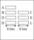
Fig. 4.4 Programmer's view of 8085 (incomplete)
4.4 ACCUMULATOR OR REGISTER A
Register A is a 8-bit register in 8085. Register A is quite often called as a Accumulator. Among the 8-bit GPRs of 8085, this is the most important. In an arithmetic operation involving two operands, one operand has to be in this register. And the result of the arithmetic operation will be stored or accumulated in this register. This justifies the name ‘accumulator’ for this register. Similarly, in a logical operation involving two operands, one operand has to be in the accumulator. Also, some operations, like complementing and decimal adjustment, can be performed only on the accumulator.
There are more ways of putting information, as well as taking out information from accumulator compared with the other registers. Technically speaking, there are more ways of addressing the accumulator compared with the other registers.
4.5 REGISTERS B, C, D, E, H, AND L
All these GPRS are 8-bits wide. They are less important than the accumulator. For example, there is no instruction to add contents of D and H registers. Atleast one of the operands has to be in A. Thus to add D and H registers, and to store the result in D register, the following have to be done.
- Move to A register the contents of D register.
- Then add A and H registers. The result will be in A.
- Move this result from A register to D register.
It is possible to use these registers as pairs to store 16-bit information. Only BC, DE, and HL can form register pairs. The instructions of 8085, for example, cannot treat the contents of C and H registers as a single 16-bit quantity. They are always treated as two separate 8-bit quantities.
The information in these register pairs can be interpreted as 16-bit data or 16-bit address of a memory location, depending on the instruction being executed. For example, in the instruction LDAX B, the contents of BC pair are treated as 16-bit memory address. In the instruction DAD B, the contents of BC pair are treated as 16-bit data. These instructions are described in the next chapter.
When they are used as register pairs in an instruction, the left register is understood to have the MS byte and the right register the LS byte. For example, in BC register pair, the content of B register is treated as the MS byte, and the content of C register is treated as the LS byte.
After the names A, B, C, D, E, why it has become H and L, instead of F and G? The reason is as follows.
As far as register pairs are concerned, HL pair is the most important. Although 8085 is a 8-bit processor, the designers have provided for 16-bit addition in the instruction set. In such a 16-bit addition, one of the operands has to be in the HL pair. Also, there are more ways of addressing the HL pair compared with the other register pairs.
In some 8085 instructions there will be a memory operand, indicated as M in an instruction. An example is ‘MOV C, M’. This instruction, to be discussed in a later chapter, stands for ‘move to C register from memory’. In this instruction, the address of memory location is understood to be specified as the contents of H and L registers. Thus, M in an instruction always stands for contents of a memory location whose address is the contents of H and L. H will have the high part or MS byte of address, and L will have the low part or LS byte of address. So, after A, B, C, D, E it was named as H and L.
- Briefly describe the evolution of microprocessors.
- What is functional pin diagram? How does it differ from the pin diagram of an IC?
- Explain the function of the RD*, WR*, ALE, IO/M* pins of 8085.
- What is the number of memory locations 8085 can address?
- The number of address pins in Intel 8086 is 20, and in Intel 80,386 it is 32. How many memory locations are they capable of addressing?
- Why LS byte of address and data are multiplexed in 8085?
- Why addresses and data are generally indicated by the user in hexadecimal notation?
- What is the function of AD7-0 pins?
- What do you understand by programmer's view of a processor?
- What is a register and its merits/demerits over a memory location?
- What is the specialty of A register over the other GPRs?
- Mention the ways B, C, D, E, H, and L registers can be used.
- What is the specialty of HL pair over the other register pairs?