29
8051 Microcontroller
![]() Main features of Intel 8051
Main features of Intel 8051
![]() Functional blocks of Intel 8051
Functional blocks of Intel 8051
![]() Program memory structure
Program memory structure
![]() Data memory structure
Data memory structure
![]() Internal RAM organization
Internal RAM organization
![]() Internal data memory organization
Internal data memory organization
![]() SFR area
SFR area
![]() Programmer's view of 8051
Programmer's view of 8051
![]() Addressing modes of 8051
Addressing modes of 8051
![]() Immediate addressing
Immediate addressing
![]() Register addressing
Register addressing
![]() Direct addressing
Direct addressing
![]() Register indirect addressing
Register indirect addressing
![]() Indexed addressing
Indexed addressing
![]() Implied addressing
Implied addressing
![]() Instruction set of 8051
Instruction set of 8051
![]() Data transfer group
Data transfer group
![]() Arithmetic group
Arithmetic group
![]() Logical group
Logical group
![]() Bit-processing group
Bit-processing group
![]() Program branch group
Program branch group
![]() Programming examples
Programming examples
![]() Shift a multi-byte BCD number to the right
Shift a multi-byte BCD number to the right
![]() Binary to BCD conversion
Binary to BCD conversion
![]() BCD to binary conversion
BCD to binary conversion
![]() BCD to binary conversion (alternative)
BCD to binary conversion (alternative)
![]() Hex to ASCII conversion
Hex to ASCII conversion
![]() Bit manipulation program
Bit manipulation program
![]() Conversion of four-digit hex to ASCII
Conversion of four-digit hex to ASCII
![]() Questions
Questions
This chapter is devoted to the study of 8051, a popular microcontroller chip of the Intel family. A microprocessor like 8085 will have ALU, control unit, and a few registers. But a microcontroller will typically have RAM, I/O ports, and timers in addition to what is generally found in a microprocessor. Many versions of microcontrollers also have on-chip ROM or EPROM, and UART. Of course, some even have ADC on the chip. Thus a microcontroller generally has all the blocks that make up a microcomputer. Building a complete microcomputer on a single chip reduces the size and cost of the application.
Microcontrollers are used in almost every electrical and electronic gadget, like televisions, VCRs, washing machines, telephones, microwave ovens, compact disk players, computer keyboards, and printers. A microcontroller is viewed as a single-chip solution to most of the small and medium-type applications. Microcontrollers are obviously more complex than microprocessors in their architecture. Thus they were developed a few years after microprocessors were developed. The first generation of microcontrollers from Intel was 8048. Intel 8051 can be treated as a second-generation microcontroller with improved features. It belongs to MCS-51 family of Intel microcontrollers.
 29.1 MAIN FEATURES OF INTEL 8051
The main features of Intel 8051 are listed as follows and details about these features are provided in the rest of this chapter and the next.
- 8-bit CPU optimized for control applications;
- Bit processing capability;
- Separate program memory and data memory spaces (Harvard architecture);
- 4 kilobytes of on-chip EPROM for program memory (range 0000–0FFFH);
- 128 bytes of on-chip data RAM (range 00–7FH);
- 64 kilobytes program memory address space. This includes 4K bytes on-chip program memory;
- 64 kilobytes data memory address space. This is excluding 128 bytes on-chip data RAM;
- 32 bi-directional and individually addressable I/O lines;
- Two numbers of 16-bit timer/counters T0 and T1;
- Full duplex UART;
- On-chip clock oscillator;
- Interrupts from six sources, two external and four internal;
- Two-level interrupt priority structure;
- Security features for EPROM parts against software piracy;
- 255 instructional opcodes, using 111 instruction types;
- 64 instruction types executed in single machine cycle of one microsecond, when crystal frequency is 12 MHz.
Intel 8051 employs Harvard type of architecture. In this type, the program memory and data memory are separated. With this feature, overlapping of program and data memory space is avoided, providing improved security for program and data.
Intel 8751 is another member of the MCS-51 family. It has 4K bytes of on-chip EPROM instead of ROM. Yet another member, Intel 8031 does not have any program memory on-chip. Thus, 8751 is an EPROM version of 8051, and 8031 is a ROM less version of 8051. Apart from the difference mentioned here, these chips have the same instruction set and internal architecture.
29.2 FUNCTIONAL BLOCKS OF INTEL 8051
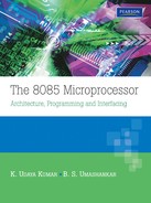
The 8051 is available in various versions as 8051H, 8051BH, and 80C51. In this book they are referred to in general as 8051. The 8051, 8031, and 8751 are available in 40-pin DIP package as well as 44-pin LCC (leadless chip carrier package with pins on all four sides of the square chip). In the LCC package four pins would be unused pins. The functional pin diagram of 8051 is provided in Fig. 29.1, and the actual pin diagram in Fig. 29.2.
The 8051 works on a power supply of +5-V dc. It has an on-chip clock circuit. All that is needed to complete the clock circuit is to connect a quartz crystal between the pins XTAL1 and XTAL2, and two capacitors as shown in Fig. 29.1. The maximum crystal frequency is typically 12 MHz. There are versions of 8051 that allow maximum crystal frequency of 20 MHz. There is a flip-flop inside 8051 that divides the clock frequency by 2, to provide the internal clock. Thus with a 12-MHz crystal, the internal clock frequency is 6 MHz. An internal clock period constitutes one state. A machine cycle of 8051 constitutes six such states, S1 to S6. Thus if the crystal frequency is 12 MHz, the duration of a machine cycle is 1μs. Most of the instructions in the instruction set of 8051 are executed in just one machine cycle.
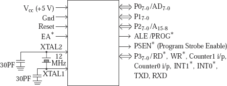
Fig. 29.1 functional pin diagram of 8051
It is also possible to drive the 8051 from an external clock source. In such a case, the clock output of the external source is connected to XTAL2 input of 8051 and XTAL1 to ground. Reset is an active high input. Logic 1 on this input for atleast two machine cycles, when the clock is running, resets the 8051.
The 8051 has four 8-bit I/O ports. The ports are called Port 0, Port 1, Port 2, and Port 3. These four ports account for 32 pins of 8051. When the internal data and/or program memory is not adequate for an application, external data and/or program memory will have to be used. In such a case, Port 2 (P2) pins provide the MS byte of address A15-0 to external memory, and P0 pins provide the LS byte of address. P0 pins are also used for data/code transfer between 8051 and external data/program memory. Thus P0 pins are used as multiplexed address data pins AD7-0. The ALE output from 8051 indicates whether address or data is present on AD7-0 pins. ALE stands for ‘address latch enable’. If logic 1 is sent out on ALE, it implies that 8051 is sending out LS byte of address on P0 pins. An external latch is used to latch this LS byte of address.
Two pins of P3 will be used for sending out read (RD*) and write (WR*) signals to external data memory. A signal with a ‘*’ after the signal name indicates that it is an active low signal. Thus RD* and WR* are active low signals. Also, if it is desired to use the internally provided timers, UART, and interrupt features, then the remaining pins of P3 will be used up for this purpose. In such a case, C0 and C1 pins are used as two counter inputs (Intel refers to them as T0 and T1), RXD and TXD pins are used by the UART for receiving and sending serial data, INT0* and INT1* are used as two external interrupt pins. Thus, only P1 is available for I/O operations when external memory is being used.
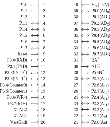
It is possible to use individually every port pin as input or output. A bit value written to a port bit comes out on the port pin. But if a port pin is to be used as an input pin, the corresponding port bit must be written with a 1 first. Only then must the port pin be read. The reason for this will become clear in the next chapter, where a detailed description of port structures is provided. In fact, after reset of 8051 all the port bits are written with 1s. Figure 29.3 provides the simplified block diagram of 8051.
Fig. 29.3 Simplified block diagram of 8051
29.3 PROGRAM MEMORY STRUCTURE
The logic level on EA* pin indicates whether the 8051 makes use of the internal program memory or not. EA* stands for ‘external access‘. If this pin is connected to logic 0, the internal on-chip ROM of 4K byte capacity will not be used. The 8051 in this case accesses only external ROM in the range 0000H–FFFFH. It is to be noted that in 8031, which is ROM less version of 8051, the EA* pin must be connected to ground.
RD* and WR* signals output by 8051 on P3 pins are used for accessing the external data memory only. So in order to facilitate reading from the external ROM, 8051 provides PSEN* output. It is an active low-output pin, which stands for ‘program strobe enable’. When PSEN* = 0, the 8051 reads from the external ROM. The 16-bit address of the external ROM location is output on P0 (LS byte) and P2 (MS byte). The program code is received on P0 pins.
If EA* is tied to logic 1, the internal on-chip ROM is used for address range 0000H–0FFFH. External ROM is accessed for addresses in the range 1000H–FFFFH. Thus it can be concluded that the total amount of program memory can be a maximum of 64K bytes including the internal program memory. The external program memory is accessed in the following cases.
- When EA* is tied to logic 0.
- When program memory in the address range 1000H–FFFFH is accessed, immaterial of logic level on EA* input.
Figures 29.4 and 29.5 provide program memory structure and interfacing of external program memory, respectively.
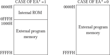
Fig. 29.4 Program memory structure
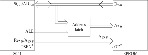
Fig. 29.5 Interfacing of external program memory
The external program memory address is always sent out as a 16-bit quantity, even if the amount of external memory is much less than 64K bytes. Thus whenever external program memory is used, P0 and P2 cannot be used for I/O purposes. The interesting aspect in the design of 8051 is that the instruction execution times do not depend on whether the instruction is in on-chip ROM or external EPROM.
29.4 DATA MEMORY STRUCTURE
The 8051 has 128 bytes of internal on-chip RAM in the address range 00H–7FH for data storage. If more data memory is needed, it is necessary to use external data memory. The data memory structure of 8051 is shown in Fig. 29.6.
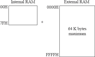
Fig. 29.6 Data memory structure
As can be seen from Fig. 29.6, it is possible to have an external data memory location with address as 50H, when there is already an internal RAM location with the same address 50H. Thus it can be concluded that the total amount of data memory can be a maximum of 64 K bytes excluding the internal data memory.
RD* and WR* signals output by 8051 on P3 pins are used for accessing the external data memory. External data memory address can be either 1- or 2-bytes wide. One-byte addresses are commonly used, but then only 256 bytes of external memory can be addressed. For most applications this should be adequate. In fact for many applications the internal program memory of 4 K bytes and internal data memory of 128 bytes should suffice. If only a little extra data memory is required, P0 pins can be used to provide an 8-bit address. Then upto 256 bytes of external data memory can be accessed. In such a case P2 is free for use as an I/O port, provided external program memory is not present.
If a little more than 256 bytes of external data memory are required, then a few lines of P2 can be used to page the external RAM. A scheme for providing 2K bytes of external data memory using eight pages of 256 bytes each is presented in Fig. 29.7.
In this scheme only three lines of P2 are used to select a page of 256 bytes. The remaining five lines of P2 can be used for I/O purposes. It is assumed that there is no external program memory. This is because if there is external program memory, 16 bits of address would have to be sent out, always on P0 and P2. In an instruction like ‘MOVX A, @R1’ (to be discussed later) only 8-bit address is sent out by 8051 on P0 pins, and it is the responsibility of the programmer to send out the three page bits using P2.
However, if a substantial amount of external data memory is required, then a full 16-bit address has to be sent out on P0 and P2. In such a case, the programmer is allowed to use instructions like ‘MOVX A, @DPTR’ (the instruction will be explained later). External program memory and external data memory may be combined if desired by connecting RD* and PSEN* outputs of 8051 as inputs to an AND gate, and using the output of AND gate as the read strobe for the external program/data memory. This scheme is shown in Fig. 29.8. In such a case it is the responsibility of the programmer to ensure that program and data occupy non-overlapping memory locations.
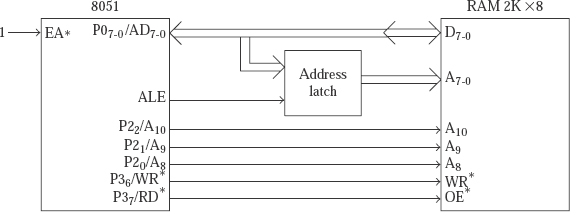
Fig. 29.7 Implementing 2k bytes of external RAM
Fig. 29.8 Circuit for common external program and data momory
29.4.1 INTERNAL RAM ORGANIZATION
Internal data memory is addressed using 8 bits. Thus 28 = 256 memory locations are possible, but 8051 contains only 128 bytes of internal data memory. They occupy the addresses 00H to 7FH. The address range 80H–FFH is allocated to accommodate a number of registers like A (accumulator), B register, DPTR (data pointer) and so on. These registers are called special function registers or SFRs. These SFRs are implemented in the internal RAM address space 80H to FFH, called the SFR space. Only 21 locations in the SFR space are used in 8051 for implementing the SFRs. The other locations in the SFR space do not exist physically. As such, the results will not be predictable if such addresses are used in an instruction. The two parts of the internal RAM are illustrated in Fig. 29.9.
29.4.2 INTERNAL DATA MEMORY ORGANIZATION
The internal data memory of 128 bytes is divided into two groups–a set of eight registers and scratch pad memory. The eight registers are R0 to R7, and are implemented in the address range 00H–07H. The rest is scratch pad memory. In fact, 8051 provides the facility of four register banks, but only one bank of registers can be in use at any point of time. Two bits in PSW (program status word), which is an SFR, selects the register bank for use. The PSW will be described later. The register banks have the following addresses.
Fig. 29.9 Data memory and SFR space in internal RAM
00H to 07H Register bank 0;
08H to 0FH Register bank 1;
10H to 17H Register bank 2;
18H to 1FH Register bank 3.
The availability of four register banks is a very useful feature for faster servicing of interrupts. The interrupted program may use one register bank, whereas the ISS may use another register bank. Hence there is no need to save and restore registers in the ISS, thus speeding up interrupt service. Even if there are nested interrupts this scheme can be used because there are four register banks.
If the user desires to use all the four register banks then only locations 20H to 7FH are available for scratch pad memory. Out of this range, memory locations 20H to 2FH can be used as bit-addressable RAM also in addition to being addressed as the usual byte locations. There are 16 bytes in this range for a total of 16×8 = 128 bits. These bits have the addresses in the range 00H to 7FH. The details are as provided in Fig. 29.10. These bits are addressed using 8 bits in an instruction like ‘CLR 78H’, which clears bit with address 78H (LS bit of location 2FH). Actually by using 8 bits it is possible to address 256-bit locations, but there are only 128 bits that are bit addressable in the internal data memory. Another 11 memory locations in the SFR area are also bit addressable. This constitutes another 88 bits that are bit addressable. They have bit addresses in the range 80H–FFH. These bit-addressable SFRs are described later. The remaining locations of the RAM in the range 30H–7FH can be used for storing variable data and implementing stack.
8051 stack: The stack in an 8051-based system is always implemented in the internal data memory. As the internal data memory range is only 00H to 7FH, the SP register is only 8 bits wide, and is one of the SFRs of 8051 with address 81H. If the user desires to use all the four register banks, and uses locations 20H to 2FH as bit-addressable memory, then the stack can start from location 30H. In such a case the SP is initialized with 2FH as is shown in Fig. 29.11.
Note that when SP contains 2FH, it means locations 2FH, 2EH, and so on upto 00H are having useful information and locations 30H, 31H, and so on upto 7FH are having useless information. Thus SP points to the highest addressed memory location having useful data. The SP is incremented by one before a push operation and is decremented by 1 after a pop operation. This is exactly the opposite of what happens to SP in 8085 microprocessor. The stack grows towards higher addresses, and variable data should be made to grow towards lower addresses. It is the programmer's responsibility to ensure that the stack and variable data do not overlap and destroy each other. As the stack is required to be implemented only in the internal data memory, only a small amount of stack is possible. This is one of the limitations of 8051.
Fig. 29.10 Organization of internal data memory
Fig. 29.11 Stack implementation in 8051
After reset of 8051, the SP is initialized to 07H. Thus locations 08H to 7FH can be used as stack area. In other words, it is assumed that only register bank 0 will be used and locations 20H to 2FH are not going to be used as bit-addressable area. However, if it is intended to use locations 20H to 2FH as bit-addressable area, then SP is initialized with 2FH.
29.4.3 SFR AREA
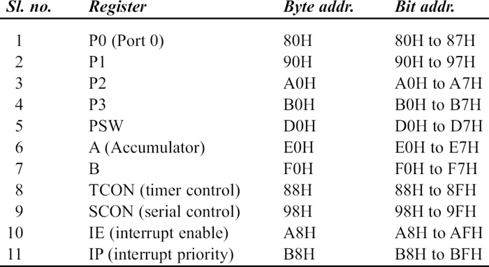
The internal RAM of 8051 has two portions, as indicated in Fig. 29.9. Locations 00H to 7FH are used for register banks, bit-addressable memory locations, stack and variable data. This has been described in the previous section. Locations 80H to FFH is reserved for SFR area. Only 21 locations in the SFR space are used in 8051 for implementing the SFRs. It is illegal to access other locations in the SFR space. Out of the 21 locations, 11 locations are bit-addressable SFR locations as are shown in Table 29.1. It may be noted that an SFR whose address has a 0H or 8H in the LS hex digit is a bit-addressable SFR.
Table 29.1 Bit-addressable SFRs
Only PSW register is described below. The other SFRs are explained later.
PSW register: The PSW register is nothing but the conventional flags register of a typical microprocessor. It is a bit-addressable SFR whose byte address is D0H. The bits in the PSW have the addresses D0H to D7H of which D7H is the address of the MS bit of PSW. Only 7 bits in the PSW are meaningful bits. The details of the PSW register are shown in Fig. 29.12.
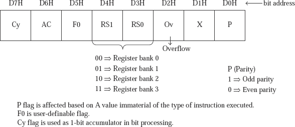
Fig. 29.12 sDetails of PSW register
The Cy flag has the usual meaning as in the case of 8085 processor. It is affected by the execution of add, subtract, and rotate through carry instructions. The Cy flag is also used as a 1-bit accumulator in bit manipulation instructions. Intel refers to bit manipulation as Boolean operations. Bit manipulation instructions are described later. The AC flag has the usual meaning as in the case of 8085 processor. The programmer does not use it, but the 8051 uses the value of this flag during the execution of DAA (decimal adjust accumulator). The V flag is useful in signed number arithmetic. If we are working with unsigned numbers there is no significance for this flag.
The P flag is set to 1 or cleared to 0 by the 8051 at the end of each instruction cycle depending on the number of 1s in the accumulator. The instruction executed need not be an arithmetic instruction. If there are even number of 1s the P flag is cleared to 0. For odd number of 1s the P flag is set to 1. Note that this is exactly the opposite of the meaning of P flag in 8085 processor.
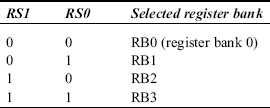
F0 is a general purpose flag bit, which is uncommitted and may be used as a general-purpose status flag. In fact, even bit D1H in the PSW can be used as a general-purpose flag. RS1 and RS0 bits in the PSW are used to select the current register bank as shown below.
Note that Z flag and sign flags are not implemented in 8051. The F0 bit, for example, can be used as sign flag. The user will have to set this bit to 1 when the MS bit of result is 1. The Z flag is not much needed because the 8051 checks for a zero or non-zero condition by testing the contents of the accumulator directly.
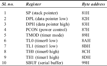
Of the 21 SFR locations, ten contain byte information, which are not bit addressable, as that would not make any sense for these SFRs. These non-bit-addressable SFRs are shown as follows. These SFRs (excluding SP, which is already discussed) will be discussed later.
After reset of 8051, the SFRs will be initialized to the following values.
- SP contains 07H.
- Ports 0 to 3 will contain FFH.
- SBUF will have indeterminate (garbage) value.
- All other SFRs will have 00H.
29.5 PROGRAMMER'S VIEW OF 8051
The programmer's view of 8051 is presented in Fig. 29.13.
From a programmer's viewpoint 8051 has the following.
- Eight registers R0 to R7 of 8-bit width; 10 commonly used SFRs listed as follows;
- Registers A and B of 8-bit width;
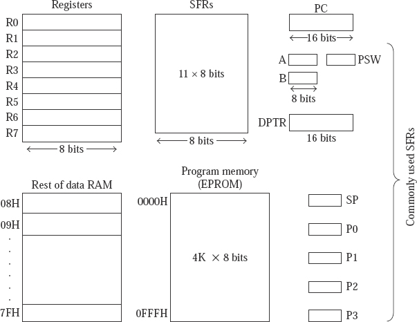
- PSW, SP, Ports P0, P1, P2 and P3-each of 8 bits;
- DPTR of 16-bit width comprising of DPH and DPL-each of 8 bits;
- Remaining 11 SFRs;
- Data RAM from 08H to 7FH;
- Program memory from 0000H to 0FFFH;
- Sixteen-bit PC.
29.6 ADDRESSING MODES OF 8051
The length of an 8051 instruction is 1, 2, or 3 bytes. However, except for a few instructions, the others are just 1- or 2-byte instructions. The opcode for an instruction is always 8 bits long. Hence 28 = 256 opcodes are possible, of which 255 opcodes have been implemented. They can be classified into 111 types of instructions. If the crystal frequency is 12MHz, then 64 instruction types are executed in just 1μs, and the rest in just 2μs (except for multiply and divide instructions that need 4μs). Intel 8051 provides the following addressing modes for accessing data from internal data memory or external data memory.
- Immediate addressing;
- Register addressing;
- Direct addressing;
- Register indirect addressing;
- Indexed addressing;
- Implied addressing.
29.6.1 IMMEDIATE ADDRESSING
In this type of addressing the source operand value is provided in the byte or bytes following the opcode, examples of which are shown in the following.
MOV A, #64H;        Moves 64H to A. 2-byte instruction.
      MOV R6, #0E3H;      Moves E3H to R6. 2-byte instruction.
      MOV DPTR, #1234H;   Moves 1234H to DPTR. 3-byte instruction.
The ‘#’ symbol stands for immediate data. DPIR stands for Data Pointer. It is a 16-bit SFR. The DPTR points to an external data memory location. If a hexadecimal value starts with A to F, it should be preceded by 0, as in 0E3. The code for the 3-byte instruction ‘MOV DPTR,#1234H’ is stored in memory as ‘90 12 34’, where 90H is the opcode for ‘MOV DPTR’. It is to be noted that 1234H is not stored in byte reversal form.
29.6.2 REGISTER ADDRESSING
In this type of addressing the source or destination operand is the contents of Rn (n 5 0 to 7). Rn is specified in the opcode using 3 bits, examples of which are shown in the following.
MOV A, R3;  Moves contents of R3 to A. 1 byte instruction.
       MOV R6, #30H;  Moves 30H to R6. 2 byte instruction.
       MOV R5, A;     Moves contents of A to R5. 1 byte instruction.
Note that there is no instruction like ‘MOV R5,R3’. The same effect is achieved using the instruction ‘MOV R5,03H’ or ‘MOV 05H,R3’. This is because, in order to provide instructions like ‘MOV R5,R3’ an additional 64 opcodes are required, and already 255 out of the possible 256 opcodes are implemented. It should be noted that ‘MOV R5,03’ works fine in place of ‘MOV R5,R3’ only if the selected register bank is 0. If we are using register bank 1, ‘MOV R5,0BH’ has to be used for the same effect.
29.6.3 DIRECT ADDRESSING
In this type of addressing, the source or destination operand address is specified using 8 bits in the instruction. Only internal data memory and SFRs can be directly addressed. In fact, SFRs are accessed using only direct addressing mode. External memory cannot be accessed using direct addressing mode in 8051. The following are some examples.
MOV 80H, R3 ; Moves contents of R3 to Port 0. P0 address is 80H.
       MOV R6, 30H ; Moves contents of internal RAM location 30H to R6.
       MOV R5, 03H ; Moves contents of R3 to R5. (Assuming Register bank is 0)
       MOV 05H, R3 ; Moves contents of R3 to R5. (Assuming Register bank is 0)
Note that ‘80H’ without ‘#’ preceding it, refers to an address. All the above instructions are 2 bytes in length. Many assemblers allow ‘MOV 80H,R3’ to be written as ‘MOV P0,R3’.
Advantage of SFR: There is a definite advantage in treating SFR as an internal RAM location instead of just treating it as a register. If a few more SFRs are added to the microcontroller in its improved version, then there is no need to add any more instruction codes to access these added SFRs. It is something like if the memory in the computer system is increased, there is no need to have additional instruction codes to access these added memory locations. To justify the above, it may be noted that 8752 is an improvement over 8051, as it has one more timer/counter. But the instruction set of 8051 and 8752 remain the same. Thus further (128–21) = 107 SFRs may be added to 8051 architecture without the need for additional instruction codes. On the other hand, if one more register, say G register, is added to 8085 architecture, then we must have additional opcodes for instructions like ‘MOV A, G’ and so on.
29.6.4 REGISTER INDIRECT ADDRESSING
In this type of addressing the source or destination operand address is provided in a register. In this mode, both internal and external data memory can be accessed. Only R0 and R1 can be used as 8-bit address registers. Only DPTR can be used as 16-bit address register. The following are some examples.
MOV 0F0H, @R1 ;Suppose (R1) = 40H. Then contents of internal RAM
                ;location 40H is moved to B. B address is F0H.
MOV @R0, 90H    ;Suppose (R0) = 30H. Then contents of Port 1 is moved
                ;to internal RAM location 30H. Port 1 has address 90H.
The ‘@’ symbol stands for register indirect addressing. The above instructions are 2 bytes in length. Note that in the assembly language R0 to R7 and all the SFRs except A, and DPTR are expressed using their 8-bit SFR address. Exceptions to this are the push and pop instructions where even A, and DPTR are expressed using their 8-bit SFR address. However, many standard assemblers provide the facility of using the SFR name in assembly language programming, although in machine language the SFR address will be used (except for A, DPTR, and R0 to R7 in general). But some assemblers expect the SFR address, instead of SFR name, to be used in assembly language also.
Thus in many assemblers ‘MOV 0F0H, @R1’ can also be written as ‘MOV B, @R1’ which is more easily understandable. Similarly, ‘MOV @R0, 90H’ can be written as ‘MOV @R0, P1’
MOVX A, @R0  ;Suppose (R0) = 40H. Then contents of external RAM
              ;location 40H is moved to A.
MOVX @DPTR, A ;Suppose (DPTR) = 1240H. Then contents of A is
              ;moved to external RAM location 1240H.
The ‘X’ in ‘MOVX’ refers to eXternal data memory. The above instructions are 1-byte long. Note that external data memory can be accessed using register indirect addressing only. Also only A register communicates with external memory.
29.6.5 INDEXED ADDRESSING
In this type of addressing the source operand is accessed from program memory only. It is intended for reading look-up tables present in program memory. The destination operand is always A register. Some examples follow.
MOVC A, @A1PC ;Suppose (A) = 20H, (PC) 5 1231H. Then contents
                ;of program memory location 1251H is moved to A.

MOVC A, @A1DPTR ;Suppose (A) = 20H, (DPTR) = 2230H. Then contents
                ;of program memory location 2250H is moved to A.
The ‘C’ in ‘MOVC’ refers to code byte. The above instructions are 1 byte in length.
29.6.6 IMPLIED ADDRESSING
In this type of addressing there will be a single operand, and this happens to be a specific register only, like the accumulator. Intel refers to this type of addressing as ‘register specific instructions’. The following are some examples.
RL A ;Rotate left A. Only A register can be rotated left / right.
      SWAP A           ;Swap nibbles in A. Swapping possible with A register only.
The above instructions are 1-byte in length.
29.7 INSTRUCTION SET OF 8051
The instructions of 8051 can be classified into the following groups.
- Data transfer group;
- Arithmetic group;
- Logical group;
- Program branch group;
- Bit-processing group (Intel calls it Boolean variable manipulation).
In an instruction that has two operands, the first operand specifies the destination and the second specifies the source. This is the same as in the Intel 8085 microprocessor.
29.7.1 DATA TRANSFER GROUP
There are 28 instruction types in the data transfer type of operations. They account for 79 opcodes, which are indicated in Table 29.2. The table indicates the mnemonic, length of the instruction, execution time in terms of machine cycles, and number of opcodes for the type of instruction. Thus, if the execution time is shown as one machine cycle, it takes 1μs for execution if the crystal frequency is 12 MHz. None of the flags are affected by the execution of data transfer instructions. However, if A value is altered because of the execution of a data transfer instruction, the P flag is set to 1 if there are odd number of 1s, else it is reset to 0. Also if data is moved to PSW register all the flags are obviously affected. In the description of instructions, the following convention is used.
Rn = any of the registers R0 to R7;
Ri = any of the registers R0 and R1;
d8 = any 8-bit immediate data (range 00H FFH);
Table 29.2 Data Transfer Group Instructions
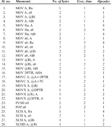
d16 = any 16-bit immediate data (range 0000H–FFFFH);
a8 = 8-bit address. This could refer to an SFR or a data RAM location.
Examples
‘MOV R3, 25H’ is a typical example for the general type of instruction ‘MOV Rn, a8’. The contents of internal RAM location 25H are moved to R3. It is a 2-byte instruction, and the execution time is two machine cycles.
‘MOV 0F0H, #25H’ is a typical example for the general type of instruction ‘MOV a8, #d8‘. The immediate data 25H is moved to register B, which is an SFR with address F0H. It is a 3-byte instruction, and the execution time is two machine cycles. The instruction can also be written as ‘MOV B, #25H’.
‘PUSH 0E0H’ is a typical example for the general type of instruction ‘PUSH a8’. The contents of A register (SFR address E0H) are pushed on the stack. The SP is incremented by 1 in this operation. It is a 2-byte instruction, and the execution time is two machine cycles. The instruction can also be written as ‘PUSH A’.
‘POP 30H’ is a typical example for the general type of instruction ‘POP a8’. The contents of stack top is moved to internal RAM location 30H. The SP is then decremented by 1. It is a 2-byte instruction, and the execution time is two machine cycles.
‘XCH A, R3’ is a typical example for the general type of instruction ‘XCH A, Rn’. The contents of A and R3 are exchanged. It is a 1-byte instruction, and the execution time is one machine cycle.
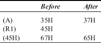
‘XCHD A, @R1’ is a typical example for the general type of instruction ‘XCHD A, @Ri’. The contents of LS digit of A and LS digit of internal RAM location pointed by R1 are exchanged. If A contents are 35H, R1 contains 45H, and internal RAM location 45H contains 67H, then A contents are changed to 37H and internal RAM location 45H contents are changed to 65H. It is a 1-byte instruction, and the execution time is one machine cycle. The effect of execution of this instruction is represented as shown below.
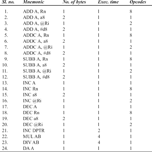
29.7.2 ARITHMETIC GROUP
There are 24 instruction types in the arithmetic group of instructions, which account for 64 opcodes. They are indicated in Table 29.3. The Cy, AC, and V flags are affected based on the result in the case of ADD, ADDC, and SUBB instructions. The multiply and divide instructions clear the Cy flag, and do not affect the AC flag. The V flag is set to 1 after multiply instruction, if the result is greater than FFH, else it is cleared. Similarly after divide instruction, the V flag is set to 1 if the B content was 00 before division, else it is cleared. DA A instruction affects the Cy flag only. Other instructions do not affect any flags. However, when A value is altered because of execution of an instruction, the P flag is affected.
Table 29.3 Arithmetic Group Of Instruction
‘ADD A, #25H’ is a typical example for the general type of instruction ‘ADD A, #d8’. The immediate data 25H is added to A, and the result is stored in A. It is a 2-byte instruction, and the execution time is one machine cycle. Note that for add and subtract instructions the result is always stored in A.
‘ADDC A, @R0’ is a typical example for the general type of instruction ‘ADDC A, @Ri’. The contents of internal RAM location pointed by R0 is added to A. It is a 1-byte instruction, and the execution time is one machine cycle.
‘SUBB A, R3’ is a typical example for the general type of instruction ‘SUBB A, Rn’. SUBB stands for subtract with borrow. The contents of R3 is subtracted from A contents along with borrow, and the result is stored in A. ‘SUBB A, R3’ is a 1-byte instruction, and the execution time is one machine cycle. Note that there is no ‘SUB A, R3’ which subtracts R3 contents from A. This was due to paucity of opcodes. If this operation is desired, then it is necessary to execute ‘CLR C’ and ‘SUBB A, R3’. ‘CLR C’ clears the Cy flag to 0.
‘INC 30H’ is a typical example for the general type of instruction ‘INC a8’. The contents of internal RAM location 30H is incremented by one. It is a 2-byte instruction, and the execution time is one machine cycle.
‘INC DPTR’ increment contents of DPTR by one. It is a 1-byte instruction, and the execution time is two machine cycles. ‘DEC DPTR’ instruction is strangely not implemented in 8051.
‘MUL AB’ multiplies the contents of A and B registers, treating them as unsigned numbers. The 16-bit result is stored in B (MS byte) and A (LS byte). If the result is larger than FFH, then the V flag is set to one. The Cy flag is always cleared after the multiply instruction. It is a 1-byte instruction that needs four machine cycles for execution.
‘DIV AB’ divides the contents of A register by the contents of B register, treating them as unsigned numbers. The 8-bit quotient is stored in A and the 8-bit remainder in B register. The V flag is set to 1 only if B content is 00H before division. Also A and B values are undefined after divide operation. The Cy flag is always cleared after the divide instruction. It is a 1-byte instruction that needs four machine cycles for execution.
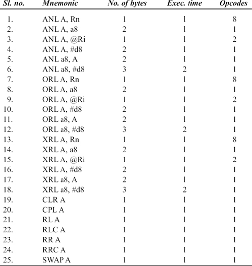
29.7.3 LOGICAL GROUP
There are 25 instruction types in the logical group of instructions. They account for 49 opcodes which are indicated in Table 29.4. Only RRC and RLC instructions affect the Cy flag. The other instructions do not affect any flag.
Examples
‘ANL A,R3’ is a typical example for the general type of instruction ‘ANL A,Rn’. The contents of R3 is ANDed with Acontents and result stored in A. It is a 1-byte instruction, and the execution time is one machine cycle. This is similar to ‘ANA’ instruction of Intel 8085. Similarly OR and Ex-OR operations can also be performed. Note that in these operations the destination operand is always A register.
‘CLR A’ instruction results in A contents becoming 00H. It is not possible to clear the contents of any other register or memory location. It is a 1-byte instruction, and the execution time is one machine cycle.
‘CPL A’ instruction results in complementing every bit of A register. It is not possible to complement the contents of any other register or memory location. It is a 1-byte instruction, and the execution time is one machine cycle.
‘RL A’ rotates left contents of A by 1-bit position. It is similar to ‘RLC’ instruction of Intel 8085, except that none of the flags are affected. Contents of no other register or memory location can be rotated left or right. ‘RL A’ is a 1-byte instruction that is executed in one machine cycle.
Table 29.4 Lagical Group Of Instruction
‘RLC A’ rotates left contents of A together with Cy flag by 1-bit position. It is the same as the ‘RAL’ instruction of Intel 8085. Only Cy flag is affected. ‘RLC A’ is a 1-byte instruction that is executed in one machine cycle.
‘RR A’ rotates right contents of A by 1-bit position. It is similar to ‘RRC’ instruction of Intel 8085, except that none of the flags are affected. ‘RR A’ is a 1-byte instruction that is executed in one machine cycle.
‘RRC A’ rotates right contents of A together with Cy flag by 1-bit position. It is the same as the ‘RAR’ instruction of Intel 8085. Only Cy flag is affected. ‘RRC A’ is a 1-byte instruction that is executed in one machine cycle.
‘SWAP A’ instruction exchanges the LS hex digit with the MS hex digit in A. It is functionally the same as executing RLA/RRA four times. The flags are not affected and it is a 1-byte instruction that is executed in one machine cycle.
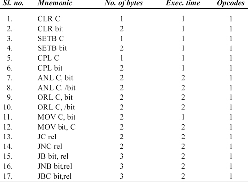
29.7.4 BIT-PROCESSING GROUP
There are 17 instruction types that come under bit processing of instructions. They account for 17 opcodes. The carry bit acts like ‘single-bit accumulator’ in many bit-processing instructions. The bit-processing instructions are indicated in Table 29.5. These instructions do not affect any flags, however, instructions like‘ANL C, bit’ will obviously affect the Cy flag. In the description of these instructions, the following convention is used.
Table 29.5 Bit Processing Instructions
bit = 8-bit address of a bit which is bit addressable;
rel = 8-bit signed displacement (range–128 to + 127) relative to first byte of the following instruction.
Examples
‘CLR C’ instruction results in Cy flag becoming 0. It is a 1-byte instruction, and the execution time is one machine cycle.
‘SETB 0D5H’ is a typical example for the general type of instruction ‘SETB bit’. It sets to 1 bit D5 (which is F0 flag in PSW). It is a 2-byte instruction, and the execution time is one machine cycle. The instruction could also be written as ‘SETB PSW.5’ or ‘SETB F0’.
‘CPL C’ instruction results in complementing C bit. Similarly using ‘CPL bit’ instruction a bit can be complemented.
‘ANL C, 07’ is a typical example for the general type of instruction ‘ANL C, bit’. It ANDs C bit with bit 7 (which is MS bit in internal RAM location 20H) and stores the result in C. It is a 2-byte instruction, and the execution time is two machine cycles.
‘ORL C, /07’ is a typical example for the general type of instruction ‘ORL C, /bit’. It ORs C bit with complement of bit 7 (bit 7 is MS bit in internal RAM location 20H) and stores the result in C. It is a 2-byte instruction, and the execution time is two machine cycles.
‘MOV C, 07’ is a typical example for the general type of instruction ‘MOV C, bit’. It moves the contents of bit 7 (which is MS bit in internal RAM location 20H) to C. It is a 2-byte instruction, and the execution time is one machine cycle.
Thus if it is required to set the Cy flag if and only if LS bit of P0 is 1, MS bit of A register is 1, and V flag is 0, the following instructions are to be executed.
MOV C, 80H   ;80H is address of LS bit of Port 0
                         ANL C, 0E7   ;E7H is address of MS bit of A register
                         ANL C,/0D2H  ;D2H is address of Overflow flag in PSW
These instructions could have been written as
MOV C, P0.0
                              ANL C, ACC.7
                              ANL C, /OV ; or ANL C, /PSW.2
‘JC LOOP’ is a typical example for the general type of instruction ‘JC rel’. If the Cy flag is set to 1, then a branch to location LOOP takes place. If Cy flag = 0, execution proceeds with the next instruction. LOOP is a symbolic location, but the assembler generates an 8-bit signed displacement from the instruction following ‘JC LOOP’. Thus branch can take place to a location which is 128 bytes behind or 127 bytes ahead of the instruction following JC. It is a 2-byte instruction, and the execution time is two machine cycles.
‘JNB 80H, BACK’ is a typical example for the general type of instruction ‘JNB bit, rel’. If LS bit of Port 0 (bit address 80H) is reset to 0, then a branch to location BACK takes place. If this bit is set to 1, execution proceeds with the next instruction. BACK is a symbolic location, but the assembler generates an 8-bit signed displacement from the instruction following ‘JNB 80H,BACK’. It is a 3-byte instruction, and the execution time is two machine cycles. The instruction could also be written as ‘JNB P0.0, BACK’.
‘JBC 80H, BACK’ is a typical example for the general type of instruction ‘JBC bit, rel’, where JBC stands for ‘jump if bit is set and then clear bit’. If LS bit of P0 (bit address 80H) is set to 1, then a branch to location BACK takes place and the bit will be cleared to 0. If this bit was reset to 0, execution proceeds with the next instruction. BACK is a symbolic location, but the assembler generates an 8-bit signed displacement from the instruction following ‘JNB 80H, BACK’. It is a 3-byte instruction, and the execution time is two machine cycles. The instruction could also be written as ‘JBC P0.0, BACK’. In reality, instructions like JC, JNB, and JBC could be discussed under program branch instructions.
29.7.5 PROGRAM BRANCH GROUP
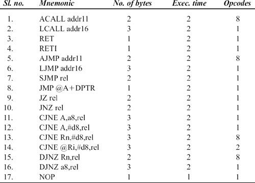
There are 17 instruction types that come under program branch instructions. They account for 46 opcodes. The program branch instructions are indicated in Table 29.6. Only CJNE instruction affects the Cy flag, while other instructions do not affect any flag. In the description of these instructions, the following convention is used.
addr11 = 11-bit address
addr16 = 16-bit address
Examples
‘LJMP LOOP’ is a typical example for the general type of instruction ‘LJMP addr16’. LJMP stands for long jump. It performs a branch to symbolic location LOOP. The assembler generates a 16-bit address corresponding to location LOOP. A branch to any location in program memory is possible using LJMP instruction. It is a 3-byte instruction, and the execution time is two machine cycles.
‘ACALL SUBR’ is a typical example for the general type of instruction ‘ACALL addr11’. It is a 2-byte instruction, and the execution time is two machine cycles. ACALL stands for absolute call. It causes a branch to subroutine at symbolic location SUBR after saving address of the next instruction on the stack top. For the purpose of ACALL and AJMP instructions, the program memory can be thought of as being divided into the following blocks of 2K bytes–0000H to 07FFH, 0800H to 0FFFH, and so on, and finally F800H to FFFFH. As an example, if the address of the instruction after ACALL is in the block 1800H to 1FFFH, then the starting address of the subroutine using ACALL is restricted to be within this block of 1800H to 1FFFH. For any address within such a block, the MS 5 bits remain the same. As an example, the MS 5 bits of 1800H and 1FFFH are 00011. This 00011 is called the block address. It provides MS 5 bits of subroutine address. Hence just 11 bits of address is enough to specify the address of subroutine within the block.
Table 29.6 Program Branch Instructions
Further, the block of 2K = 0800H bytes of memory can be thought of as being divided into eight pages each of 256 = 100H bytes. Hence to select a location in a block of 2K bytes, we have to select a page within the block using 3 bits, and a location within the page using 8 bits. The ACALL instruction is implemented using only 2 bytes. The first byte will be PPP 10001, where PPP indicates page number within the block, and 10001 is the code for ACALL. The second byte contains the address within the page.
As an example, consider ‘ACALL SUBR’ being at location 1834H in external program memory. If SUBR is location 1C85H, ‘ACALL SUBR’ is coded as follows. First byte will be 100 10001B = 91H, where 100 indicates select page 4 within the block and 10001 is the opcode for ACALL. The second byte will be 85H that provides the LS byte of subroutine address.
The MS 5 bits of subroutine address will be the block address. This is 00011 as described earlier. The next 3 bits provide page address. This will be 100 to indicate page 4 within block 00011. Thus, branch takes place to the subroutine at address 00011 100 85H = 1C85H. If SUBR is at location 1D85H, then ‘ACALL SUBR’ is coded as follows. First byte will be 101 10001B = B1H, where 101 indicates select page 5 within the block and 10001 is the opcode for ACALL. The second byte will be 85H that provides the LS byte of subroutine address.
The MS 5 bits of subroutine address will be 00011 that gives the block address. The next 3 bits will be 101 to indicate page 5. Thus, branch takes place to the subroutine at address 00011 101 85H = 1D85H. From the above it should be clear that there are eight opcodes for ACALL instruction depending on the page number within the block where the subroutine starts. As can be seen, two of the eight possible opcodes for ACALL are 91H and B1H.
‘SJMP LOOP’ is a typical example for the general type of instruction ‘SJMP rel’. SJMP stands for short jump. ‘SJMP LOOP’ causes a branch to location LOOP. LOOP is a symbolic location, but the assembler generates an 8-bit signed displacement from the instruction following ‘SJMP LOOP’. It is a 2-byte instruction, and the execution time is two machine cycles. In the instruction set of 8051 there is no HALT instruction. Thus, to terminate a program ‘LOOP: SJMP LOOP’ is used.
It can be noted from Table 29.6 that there are three kinds of unconditional jumps–SJMP, AJMP, and LJMP. However, JMP is a generic name that can be used if the programmer does not care which way the jump is encoded. However, some assemblers expect atleast one of SJMP, AJMP, or LJMP to be used. Similarly, it can be noted that there are two kinds of unconditional calls–ACALL and LCALL. However, CALL is a generic name that can be used if the programmer does not care which way the call is encoded. However, some assemblers expect ACALL or LCALL to be used. There is no SCALL instruction in 8051.
‘JZ BACK’ is a typical example for the general type of instruction ‘JZ rel’. If A register contents is 00H, then a branch to location BACK takes place. If A register contents are unequal to 00H, execution proceeds with the next instruction. BACK is a symbolic location, but the assembler generates an 8-bit signed displacement from the instruction following ‘JZ BACK’. It is a 2-byte instruction, and the execution time is two machine cycles. It is to be noted that JZ instruction tests the contents of A register for a 00H value, and there is no Z flag in 8051.
The RET instruction functions as pop from stack top to PC. It is similar to the RET instruction of 8085 (except that after the RET instruction of 8051, the SP value is decremented by 2). It is an 1-byte instruction that is executed in two machine cycles.
The RETI instruction also functions as pop from stack top to PC. In addition, it restores the interrupt logic to accept additional interrupts at the same priority level as the one just processed. RETI stands for return from interrupt. An interrupt service routine ends with RETI, and an ordinary subroutine ends with RET instruction. RETI is a 1-byte instruction that is executed in two machine cycles. The use of RETI would become clear after 8051 interrupt system is described in detail later.
‘DJNZ 80H, BACK’ is a typical example for the general type of instruction ‘DJNZ a8, rel’. DJNZ stands for ‘decrement and jump if not zero’. The P0 (address 80H) contents are decremented by 1. If it is not 00H after the decrement, then a branch to location BACK takes place. Otherwise execution proceeds with the next instruction. BACK is a symbolic location, but the assembler generates an 8-bit signed displacement from the instruction following ‘DJNZ 80H, BACK’. It is a 3-byte instruction, and the execution time is two machine cycles. The instruction could also be written as ‘DJNZ P0, BACK’.
‘CJNE R3,#80H,BACK’ is a typical example for the general type of instruction ‘CJNE Rn,#d8, rel’. CJNE stands for ‘compare and jump if not equal’. The CJNE instruction combines compare and jump into a single compact instruction. In this case, R3 contents are compared with 80H. If R3 contents are different from 80H then a branch to location BACK takes place. Otherwise execution proceeds with the next instruction. BACK is a symbolic location, but the assembler generates an 8-bit signed displacement from the instruction following ‘CJNE R3,#80H, BACK’. It is a 3-byte instruction, and the execution time is two machine cycles. However, 8051 does not have instructions like ‘compare and jump if above’ or ‘compare and jump if below’.
29.8 PROGRAMMING EXAMPLES
The programming examples provided here are only to familiarize the reader with the instruction set of 8051, especially with those that are new to 8051 compared to 8085. These programs were tested on SDA 31 kit manufactured by M/s Advanced Electronic Systems, Bangalore—560 055.
29.8.1 SHIFT A MULTI-BYTE BCD NUMBER TO THE RIGHT
Write an 8051 assembly language program to shift an 8-digit BCD number by two digits to the right. The 8-digit BCD number is assumed to be in internal data memory locations 20H, 21H, 22H, and 23H. Location 20H is having the MS byte.
For the trace that follows, it is assumed that the BCD number is 12 34 56 78, with 12 at location 20H. After the program is executed, contents of location 20H is cleared to 00H, and the LS byte shifted out will be available in A.
CLR A     ;   (A) = 00
      XCH A,20H ; (20H) = 00, (A) = 12,
      XCH A,21H ; (21H) = 12, (A) = 34,
      XCH A,22H ; (22H) = 34, (A) = 56,
      XCH A,23H ; (23H) = 56, (A) = 78
STOP: SJMP STOP
29.8.2 BINARY TO BCD CONVERSION
Write an 8051 assembly language program to convert an 8-bit binary number to its equivalent BCD value. The 8-bit binary number is at external RAM location 30H. The result is to be stored in locations 31H and 32H, with 31H having the MS portion of result.
In the trace that follows it is assumed that the data at location 30H is FEH. The program converts binary value FEH to BCD value of 0254, and stores it in locations 31H and 32H.
MOV P2, #00H       ;Set MS byte of external data address as 00
      MOV R0, #30H   ;Load R0 with address of data

      MOVX A, @R0    ;(A) = FEH (254 decimal)
      MOV B, #0AH    ;(B) = 0AH (10 decimal)

      DIV AB         ;(A) = 19H (25 decimal), (B)= 04
      MOV R2,  B     ;(R2) = 04

      MOV B, #0AH    ;(B) = 0AH
      DIV AB         ;(A) = 02, (B) = 05

      INC R0         ;(R0) = 31H
      MOVX @R0, A    ;(0031) = 02 (Store MS portion of result)

      MOV A, B       ;(A) = 05
      SWAP A         ;(A) = 50
      ADD A, R2      ;(A) = 54

      INC R0         ;(R0) = 32H
      MOVX @R0, A    ;(0032) = 54 (Store LS portion of result)
EXIT: SJMP EXIT      ;Stop
 29.8.3a BCD TO BINARY CONVERSION
Write an 8051 assembly language program to convert a two-digit BCD number to its equivalent binary value. The two-digit BCD number is at external RAM location 200H. The result is to be stored in location 201H.
In the program that follows, two software up counters are made use of. They start from 00 value initially. One counter counts up in decimal using A register, while the other counter counts up in binary using R2 register. When the decimal up counter reaches the desired BCD value, the count up is stopped. At that point the binary counter will have the equivalent binary value.
In the trace that follows it is assumed that the data at location 200H is 15. The program converts BCD value 15 to binary value of 0FH, and stores it in location 0201H.
MOV DPTR, #0200H ;(DPTR) = 0200H
      MOVX A, @DPTR  ;(A) = 15
      MOV R3, A      ;(R3) = 15

      CLR A          ;(A) = 00
      MOV R2, #00    ;(R2) = 00

LOOP: ADD A, #01     ;(A) = 01, 02, .., 09, 0A, 11, .., 15
      DAA            ;(A) = 01, 02, .., 09, 10, 11, .., 15
      INC R2         ;(R2)= 01, 02, .., 09, 0A, 0B, .., 0F
      CJNE A,03H,LOOP ;Repeat till A value becomes same as R3

      INC DPTR       ;(DPTR) = 0201H
      MOV A, R2      ;(A) = 0FH
      MOVX @DPTR, A  ;(0201) = 0FH
EXIT: SJMP EXIT      ;Halt
29.8.3b BCD TO BINARY CONVERSION (ALTERNATIVE)
Write an 8051 assembly language program to convert a two-digit BCD number to its equivalent binary value. The two-digit BCD number is at external RAM location 200H. The result is to be stored in location 201H. In the program shown as follows, the MS digit of the BCD number is multiplied by 10 (0AH). For example, if the BCD number is 95, 9 is multiplied by 0AH, to get 5AH. Then the LS digit of the BCD number, which is five, is added to get 5FH which is the binary equivalent of the BCD number 95.
In the following trace it is assumed that the data at location 200H is 95. The program converts BCD value 95 to binary value of 5FH, and stores it in location 0201H.
MOV DPTR, #0200H ; (DPTR) = 0200H
      MOVX A, @DPTR ; (A) = 95
      MOV R2, A     ; (R2) = 95

      SWAP A        ; (A) = 59
      ANL A, #0FH   ; (A) = 09H

      MOV B, #0AH   ; (B) = 0AH
      MUL AB        ; (A) = 5AH, (B) = 00H

      ANL R2, #0FH  ; (R2) = 05H
      ADD A, R2     ; (A) = 5FH

      INC DPTR      ; (DPTR) = 0201H
      MOVX @DPTR, A ; (0201) = 5FH
HALT: SJMP HALT     ; Stop
29.8.4 HEX TO ASCII CONVERSION
Write an 8051 assembly language program to convert a single-digit hexadecimal number to its equivalent ASCII value. The single-digit hexadecimal number is at external RAM location 300H. The result is to be stored in location 301H.
In the following trace it is assumed that the data at location 300H is 00. The program converts hexadecimal value 00 to ASCII value of 30H, and stores it in location 0301H. The program uses look-up table approach. Immediately after the RET instruction, the look-up table containing the ASCII codes for ‘0’ to ‘F’ is stored.
In the CONVRT subroutine when ‘MOVC A, @A+PC’ is executed, the PC value taken for calculation is the address of RET instruction. So to move past the 1-byte RET instruction and fetch result from look up table, A value is incremented by 1 in the main program before branching to CONVRT subroutine.
MOV DPTR, #0300H   ;(DPTR) = 0300H
        MOVX A, @DPTR      ;(A) = 00H
        INC A              ;(A) = 01H

        ACALL CONVRT       ;(A) = 30H

        INC DPTR           ;(DPTR) = 0301H
        MOVX @DPTR, A      ;(0301) = 30H
STOP:   SJMP STOP ;Halt

CONVRT: MOVC A, @A+PC      ;(A) = 30H
        RET                ;Return to main program

        30H  ;ASCII code for ‘0’
        31H
        32H
        33H
        34H
        35H
        36H
        37H
        38H
        39H  ; ASCII code for ‘9’
        41H  ; ASCII code for ‘A’
        42H
        43H
        44H
        45H
        46H  ; ASCII code for ‘F’
29.8.5 BIT MANIPULATION PROGRAM
Write an 8051 assembly language program to modify a given byte at internal RAM location 40H as detailed below, and store the modified byte at internal RAM location 41H.
Bit 0 is to be set to 1;
     Bit 2 is to be reset to 0;
     Bit 4 is to be complemented;
     Bit 6 value should become the same as bit 5;
     Bit 7 value should become AND of bit 1 and complement of bit 3.
In the trace that follows, it is assumed that the data at internal RAM location 40H is 25H. The program modifies it to 71H and stores it in internal RAM location 41H.
In the program that follows, contents of internal RAM location 40H is moved to internal RAM location 20H, which is a bit-addressable RAM location. This is done in order to carry out bit manipulation on this byte. In this program ‘MOV C, 20.5’ stands for ‘move to Cy flag bit 5 of byte at internal RAM location 20H’. It could as well have been written as ‘MOV C, 5’.
MOV 20H, 40H ;(20H) = 0010 0101

      SETB 20.0     ;(20H) = 0010 0101
      CLR 20.2      ;(20H) = 0010 0001
      CPL 20.4      ;(20H) = 0011 0001

      MOV C, 20.5   ;(C) = 1. It can be written as ‘MOV C, 5’ also.
      MOV 20.6,C    ;(20H) = 0111 0001

      MOV C, 1      ;(C) =0. It can be written as ‘MOV C,20.1’ also.
      ANL C, /3     ;(C) = (0 AND 1) = 0
      MOV 7, C      ;(20H) = 0111 0001 = 71H

      MOV 41H, 20H  ;(41H) = 71H
EXIT: SJMP EXIT
29.8.6 CONVERSION OF FOUR-DIGIT HEX TO ASCII
Write an 8051 assembly language program to convert a four-digit hexadecimal number to equivalent ASCII. The four-digit hex number is at internal RAM locations 30H and 31H. The equivalent ASCII is to be stored in four internal RAM locations starting from 50H.
MOV R0, #30H ;(R0) = 30H
       MOV R1, #40H ;(R1) = 40H
       MOV R2, #02H ;(R2) = 02H. R2 is used as loop counter.

;The ‘REPT’ loop converts a 4 digit hexadecimal number, say,
;12CD at internal RAM locations 30H and 31H to 01, 02, 0C, 0D, and
;stores them in locations starting from internal RAM location 40H.
REPT: MOV A, @R0  ;
      ANL A, #0F0H;

      SWAP A      ;
      MOV @R1, A  ;

      MOV A, @R0  ;
      ANL A, #0FH ;

      INC R1      ;
      MOV @R1, A  ;

      INC R0      ;
      INC R1      ;
      DJNZ R2,REPT;

      MOV R0, #40H;
      MOV R1, #50H;
      MOV R2, #04H; R2 is used as loop counter
;The ‘AGAIN’ loop converts the hex number pointed by R0 to its
;equivalent ASCII, and stores in location pointed by R1. This
;is done by adding 30H to hex number, if the number is in the
;range 0 to 9. If the number is in the range A to F, 37H is
;added. The loop is repeated 4 times.

AGAIN: MOV A,@R0
       ADD A, #30H
       CJNE A, #3AH,FRWD

FRWD: JC NUMB
      ADD A, #07H
NUMB:  MOV @R1, A
       INC R0
       INC R1

       DJNZ R2, AGAIN
EXIT:  SJMP EXIT
In the previous program it should be noted that the following two instructions of 8051
CJNE A, #3AH,FRWD
                         FRWD: JC NUMB
are equivalent to the following 8085 instructions:
CPI 3AH
       JC NUMB
- What is a microcontroller? What are its typical applications?
- Mention the salient features of the 8051 microcontroller.
- Explain the functional pin diagram of 8051 with a neat diagram.
- Describe program memory structure. With a neat diagram explain interfacing of external program memory.
- Describe data memory structure.
- With a neat diagram explain interfacing of 2K bytes of external data memory.
- Describe internal RAM organization in 8051.
- Explain the various bits available in PSW register.
- What happens to various register contents in 8051 after reset?
- Describe the programmer's view of 8051.
- Explain with examples the various addressing modes of 8051.
- Mention the various types of instructions available for 8051, with examples.
- Explain the working of the following instructions of 8051.
- XCH A, 40H
- XCHD A, @R1
- MOVX A, @DPTR
- SWAPA
- MUL AB
- DIV AB
- MOVC A,@A+PC
- CLR C
- DJNZ R3, BACK
- CJNE A, 40H, LOC
- ANL C,/50H
- JBC 50H, LOOP